EP0092676A2 - Méthode de mesure de temps et dispositif pour son application - Google Patents
Méthode de mesure de temps et dispositif pour son application Download PDFInfo
- Publication number
- EP0092676A2 EP0092676A2 EP83102782A EP83102782A EP0092676A2 EP 0092676 A2 EP0092676 A2 EP 0092676A2 EP 83102782 A EP83102782 A EP 83102782A EP 83102782 A EP83102782 A EP 83102782A EP 0092676 A2 EP0092676 A2 EP 0092676A2
- Authority
- EP
- European Patent Office
- Prior art keywords
- signal
- time
- converter circuit
- delay
- amplitude converter
- Prior art date
- Legal status (The legal status is an assumption and is not a legal conclusion. Google has not performed a legal analysis and makes no representation as to the accuracy of the status listed.)
- Granted
Links
Images


Classifications
-
- G—PHYSICS
- G01—MEASURING; TESTING
- G01R—MEASURING ELECTRIC VARIABLES; MEASURING MAGNETIC VARIABLES
- G01R25/00—Arrangements for measuring phase angle between a voltage and a current or between voltages or currents
-
- G—PHYSICS
- G04—HOROLOGY
- G04F—TIME-INTERVAL MEASURING
- G04F10/00—Apparatus for measuring unknown time intervals by electric means
Definitions
- the invention relates to a time measurement method according to the preamble of claim 1.
- the two time measuring repeatable individual signals two time marker signals whose temporal b A-stand is to be determined as precisely as possible.
- the measured value in question is not obtained directly, but arithmetically from three individual measured values, a so-called rough measurement value and two so-called fine measurement values.
- the coarse measurement value is obtained by counting the periods of a time base signal that occurred between the two time mark signals, which is supplied by a free-running, ie crystal-controlled oscillator that is in no way correlated or synchronized with the two time mark signals.
- the two fine measurement values which each indicate the time interval between the earlier or later time mark signal to a subsequent, e.g.
- a typical application example for this known time measurement method is represented, for example, by distance measurement methods based on the principle of time-of-flight measurement of a light pulse, in which the light pulse emitted by a transmitter light source is divided within the measuring device into a measurement light pulse and a reference light pulse, the former emitting to the target object via the transmitter optics, from there it is reflected to the measuring device and is passed in the measuring device to a light receiver which has previously received the reference light pulse via a short, internal reference light path of known length. Both light pulses trigger two signals in the evaluation circuit following the light receiver, which represent the time stamp signals of the time measurement method described above and whose time interval is a measure of the distance of the target object.
- each of these two individual signals initially generated at the same time is subject to its own delay, which differs from that of the other signal.
- the delays of these two signals also remain unchanged when the light pulse is generated again.
- Another application for a time measuring method the measurement of phase shift between two periodic signals of the same frequency.
- this is periodic square-wave signals, so two consecutive within a period length stei- f end Flanks of one and the other periodic signal, the repeatable individual signals and the phase shift between the two periodic signals can be measured by the time intervals of these repeatable individual signals from a subsequent defined, for example the next rising edge of a time base signal having the same frequency measures, the difference between these two time intervals then being included in the measurement result of interest.
- the main difference from the time measurement method known from DE-OS 30 12 186.9 here is that only the two so-called fine measurement values, but not a coarse measurement value, are determined.
- the sum of the different delays to which the two repeatable individual signals are subjected before the time measurement results in the phase shift to be measured.
- These two delays do not have to be caused by the fact that the two signals resulting from the periodic repetition of the individual signals were generated simultaneously, ie without phase shift, and then traveled through paths of different lengths. Instead, the different delays can also be imprinted on the two periodic signals right from the start, that is, when they are generated.
- the time intervals are measured with one and the same time / amplitude converter circuit, and if the measured values to be subtracted are obtained quickly enough in succession, not only long- and medium-term drift phenomena, but also short-term fluctuations due to the difference are eliminated.
- this circuit is to be continuously verified using a calibration standard, for which purpose the period length of the time base signal is well suited, for example, if the time base signal is generated with the aid of a quartz-controlled oscillator.
- only individual points of the time / amplitude converter circuit characteristic curve can be detected in this way, which are each exactly spaced from one another by a period length of the time base signal.
- the characteristic curve areas located between these points which are of particular importance because the time intervals to be measured generally do not represent an integral multiple of the period length of the time base signal, are shown bridged by a simple linear interpolation between the calibration measuring points.
- the characteristic of the time / amplitude converter circuit between the calibration measuring points can have such strong nonlinearities that when measuring the time intervals of two individual signals with subsequent difference formation, at least when very high accuracy is required, Unauthorized errors can occur, since the two measured values generally lie at different points on the points / time / amplitude converter circuit, so that they contain different parts of the error that are no longer mutually exclusive due to the non-linearity of the characteristic .
- the invention has for its object to develop a method of the type mentioned so that despite the presence of unknown non-linearities of the characteristic of the time / amplitude converter circuit, measurement results can be obtained with very high accuracy within very short periods of time.
- the invention provides the features set out in claim 1.
- the intolerably large measurement errors caused by the nonlinearities of the characteristic of the time / amplitude converter circuit and occurring in individual measurements are reduced in the required manner in that several, namely n measurements for each of the two individual signals are carried out and averages are formed from the measurement results.
- the statistical error reduction which is only effective if the time base signal is in no way correlated with the individual signals, so that each measurement results in different measured values, which are statistically distributed in their size and therefore also contain errors of different sizes. is in the method according to the invention for a coupling between the generation of the individual signals and the time base signal concerned.
- a suitable choice of the individual n-1 delay values ensures, according to the invention, that n measured values are obtained for a single signal, which are distributed evenly, ie approximately equidistantly over the / calibrated characteristic range of the time / amplitude converter circuit, so that all of them Non-linearity of the time / amplitude converter circuit characteristic possible error contributions can be detected approximately uniformly. Since the same then also occurs with the n individual signals of the other signal group, each of the n-1 different delay values used in the first signal group being used a second time, the non-linearity errors in the two measured value groups to be subtracted from one another are in the same way with very good approximation included so that they largely fall out in the subsequent subtraction and averaging.
- the calibration of the characteristic curve of the time / amplitude converter circuit is carried out with the aid of a periodic signal emitted by a quartz-controlled oscillator, for example the frequency specified above, an accuracy of 10 and better can be achieved overall, the measurement error being less than 10 ps.
- a particular advantage of the method according to the invention can be seen in the fact that it works with the accuracy just described even if the characteristic of the time / amplitude converter circuit in the calibrated area deviates from the ideal linear course only on one side, i.e. systematically delivers only too large or too small values.
- a further increase in measurement accuracy is possible according to the invention in that the individual signals of the two signal groups are generated in such a way that the time / amplitude converter circuit is operated periodically as precisely as possible.
- the characteristic curve of the time / amplitude converter circuit can then be reproduced to a particularly good degree, so that the errors in the averaging and difference formation present in the individual measurements stand out even better than is the case with aperiodic operation of the time / amplitude converter circuit is.
- these calibration measurements are also advantageously controlled in such a way that periodic operation of the time / amplitude converter circuit results at least over one signal group, which is then also carried out with the other signal group at the same frequency.
- a particularly simple construction and a particularly simple control of the delay arrangement for the individual signals used to generate the different delay values are obtained when the n-1 selected delay values each form an integer multiple of a unit delay ⁇ o, and the delays to which the n- 1
- Signals are subjected to a signal group, arranged in ascending or descending order, so that, for example, the first of n signals without delay, the second with a delay ⁇ O , the third with a delay 2x ⁇ o , etc., or in reverse order of Time / amplitude converter circuit is supplied.
- the equality of the delay values ⁇ o achievable per delay stage of the controllable delay arrangement is advantageous, but not particularly critical. Deviations in the order of magnitude of + 30% can be tolerated without further ado in order to achieve the accuracy specified above.
- the time / amplitude converter circuit being started with each calibration measurement by an edge serving as a start signal or sine zero crossing) of the time base signal and a subsequent edge serving as a stop signal (or Sine zero crossing) of the time base signal is stopped again.
- the two types of calibration measurements differ in that the start and stop signals actually supplied to the time / amplitude converter circuit differ in length, for example three period lengths of the time base signal in one type of calibration measurement and four period lengths in the other type of calibration measurement Time base signal are spaced apart.
- the two "endpoints" obtained in this way span the calibrated area of the
- the time / amplitude converter circuit works in all time interval measurements for a period of time whose length corresponds to at least three and at most slightly more than four period lengths of the time base signal.
- the calibrated range of the characteristic curve of the time / amplitude converter circuit is selected such that its temporal length is equal to a period length of the time base signal, and that it lies approximately between the points of the characteristic curve that a work Period of the time / amplitude converter circuit between three and four period lengths correspond.
- the calibrated characteristic curve range is shifted slightly towards these two points in the direction of longer working hours, which is done with the aid of a delay element which is between the stop signal output of the second.
- Edge enable circuit which is connected downstream of the start / stop control which controls the two types of calibration measurements and which is connected to the stop input of the time / amplitude converter circuit.
- the value of the delay provided by this delay element is dimensioned such that it is equal to the response delay of the input stage of the first edge enable circuit. This has the following purpose: Each individual signal is applied to the time / amplitude converter circuit and to the first edge enable circuit at the same time.
- time / amplitude converter circuit While the time / amplitude converter circuit then immediately begins measuring operation, if the individual signal is very close to the next rising (or falling) edge of the time base signal, it can happen that the first edge enable circuit due to the response delay of its input stage this edge is no longer detected and thus only releases the fifth rising (or falling) edge of the time base signal as a stop signal for the time / amplitude converter circuit. Since in these cases the time / amplitude converter circuit operates somewhat longer than four period lengths of the time base signal, it could be "backward", i.e., without the above-mentioned shift of the calibrated characteristic range. towards the longer times, the measured value falls out of the calibrated area to the rear and thus deteriorates the accuracy of the final measurement result.
- the method according to the invention can also be used with great advantage wherever the desired measured value formation includes the difference in transit times which require a first or a second repeatable individual signal from its generation to its entry in the time measurement circuit.
- the time / amplitude converter circuit and the entire measurement channel cannot be operated at a constant frequency, because the transit times to be measured contain the measurement result of interest and are therefore variable, and the time / amplitude converter circuit a three-part time measurement is generally operated at shorter intervals than from a three-part time measurement to the next.
- this aperiodic operation of the measuring channel results in a deterioration in the accuracy of the measurement results obtained in this way.
- the method according to the invention offers the possibility of determining such transit time differences as set out in claim 19.
- the trigger signal for each individual signal is correlated in a phase-locked manner with the time base signal, it suffices to eliminate only the rough measurement values described above for at least one individual signal of one signal group and one individual signal of the other signal group, and according to claim 1, without the respective first fine measurement formation described above to determine the fine measurement values of all individual signals of both signal groups in order to obtain the desired transit time difference with the accuracy with which the period of the time base signal is constant and known.
- By eliminating the "front" fine measurement value formation it is possible to obtain the individual signals at the input of the time measurement circuit in strict periodicity by selecting the times at which the trigger signals are generated, even if the individual signals of the different signal groups have very different transit times and generated alternately.
- the delay between the time of generation of the at least two individual signals for which a coarse measurement value is determined and the subsequent (or preceding) edge of the time base signal with which the period counting is started has no effect on the measurement result is that, in the short period of time within which these individual signals can be generated, it can with certainty be regarded as constant and thus stands out in the subsequent difference formation.
- this carry is preferably controlled in such a way that it or its end signal, which holds the instantaneous output voltage of the time / amplitude converter circuit in the sample-and-hold circuit, is strictly synchronized with the time base signal.
- the time base signal everywhere, and thus also on the line connecting the output of the time / amplitude converter circuit to the input of the sample-and-hold circuit, is very small the output voltage of the time / amplitude converter circuit there is a noticeable interference signal.
- the amplitude profile of this interference signal is exactly synchronized with the time base signal, so that the synchronous control of the transfer of the analog measurement voltage from the time / amplitude converter circuit to the sample-and-hold circuit results in an error component that is always the same, which in the case of later subtraction of the measured values falls out again.
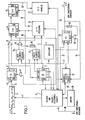
- a time measuring device has a quartz-controlled oscillator 1, which supplies the time base signal with a frequency of, for example, 15 MHz.
- This time base signal is fed via lines 2 to all those circuit parts which are to generate or pass on signals which are synchronized with the time base signal in some way.
- the entire circuit arrangement is from a central computing and sequence control unit 3 according to the requirements of the respective controlled gene measuring task, in the context of which the time measuring device is used.
- the individual signals are fed into the time measuring device according to FIG. 1 via input E. From there they arrive directly at a controllable delay arrangement 5, on whose output line 6 these individual signals with a delay 0 depending on a signal given by the computing and sequence control unit 3 via line 7 to the controllable delay arrangement 5.
- ⁇ O , ie appear without delay or with a delay that is an integer multiple of the unit delay X ".
- An individual signal thus delayed arrives via line 6 at the clock input of a flip-flop 8, which has previously been sent via OR gate 9 either with the aid of a master reset pulse emitted by computing and sequence control unit 3 or with the aid of one from a buffer store Control 10 output reset pulse has been brought into the reset state.
- the Q output of the flip-flop 8 which was previously at logic 0, opens with the rising edge of the individual signal supplied on line 6 logical 1 set.
- the resulting rising edge on the one hand reaches via the OR gate 12 to the start input of a time / amplitude converter circuit 14, which then begins the measurement process, and to a trigger input of the buffer control 10, and on the other hand to the trigger input of a first one Edge enable circuit 15, which receives the time base signal at its second input via line 2 and after triggering by the Q output Signal of the flip-flop 8 counts the rising edges of the time base signal and supplies the fourth edge via the OR gate 16 to the stop input of the time / amplitude converter circuit 14, which thereby stops its measuring operation and maintains the output voltage reached until under the direction of the buffer control 10, this is taken over into a sample-and-hold circuit 17 serving as an analog buffer.
- the sample-and-hold circuit 17 is supplied with a corresponding control signal
- the buffer controller 10 emits a reset signal via the line 19, by means of which the time / amplitude converter circuit 14 and, as already mentioned above, the D flip-flop 8 are reset to their respective initial state, in which they are ready for the processing of the next individual signal coming in via input E.
- the analog measurement result present at the output of the sample-and-hold circuit 17 reaches an analog / digital converter 22 via the line 20, which converts it into a digital form under the direction of the computing and sequence control unit 3 and this digital value to the computing and sequence control unit 3 for further processing via the bidirectional line 923, on which it also receives its control commands.
- the computing and sequence control unit 3 processes the measurement results obtained in this way and the calibration measurement values obtained in a similar manner and calculates the measurement result that is actually of interest, which can be displayed on a display unit 25.
- a D flip-flop 26 is shown, the D input of which is connected to the central computing and sequence control unit 3 via a line 27 given times can be supplied with a logical 1.
- This D flip-flop 26 represents the simplest form of a synchronization circuit, which is provided according to the invention, so that whenever the corresponding preparatory signal has been emitted via the line 27 from the computing and sequence control unit 3, an exact to the time base signal To deliver a defined phase position trigger signal for a generator (not shown in FIG. 1), which thus generates the individual signals that appear later at input E in a strictly phase-locked correlation to the time base signal.
- the time base signal of the oscillator 1 is fed to the clock input of the D flip-flop 26 via the corresponding line 2.
- the preparation signals emitted by the arithmetic and sequence control unit 3 for triggering a synchronized trigger signal are generated at the required time intervals so that the individual signal generator first generates n, ie for example eight individual signals of the first and then n, that is again eight individual signals of the second type .
- the information required for this can again be obtained from the computing and process Control unit 3 are supplied, as indicated by line 30.
- each of these individual signals on the way from the signal generator to the input E of the time measuring circuit is subject to a certain delay, the size of which is unknown, the same for the individual signals of a signal group and generally different from signal group to signal group.
- the corresponding measured values can be obtained with the aid of a counter 32, which transmits this via line 2 Receives time base signal of the oscillator 1 and counts its relevant (ie either the rising or the falling) edges.
- the start of counting of counter 32 is triggered by synchronization flip-flop 26 via line 34.
- the count result can be via the bidirectional lines 33 can be transferred from the counter 32 into the computing and sequence control unit 3.
- the counting operation of the counter 32 for each individual signal is ended by the output signal of the OR gate 16, which also stops the time / amplitude converter circuit.
- this output signal of the OR gate 16 is fed to the arithmetic and sequence control unit 3 in order to indicate that the counting result can now be taken over by the counter 32 on the lines 33.
- a start-stop control 35 is provided, which, depending on whether it is from the computing and sequence control unit 3 at its input E1 or at its input Input E2 a trigger receives signal, can carry out two different calibration measurements.
- the time / amplitude converter circuit 14 Due to this triggering via the input E1 of the start-stop control 35, the time / amplitude converter circuit 14 thus operates for a period that is somewhat longer than three periods of the time base signal and thus provides a first measured value suitable for establishing a calibration line, since yes the period length of the time base signal supplied by the quartz-controlled oscillator 1 is known with very high accuracy and is constant.
- the arithmetic and sequence control unit 3 applies a trigger signal to the input E2 of the start-stop control 35, it generates a start and a stop signal again at its two outputs, but this time this time by exactly one period length of the time base signal are offset from each other. They are supplied in the same way as described above to the time / amplitude converter circuit 14, which in this second type of calibration measurement is for a time space works that is slightly longer than four period lengths of the time base signal.
- a controllable delay arrangement 5 is used in the method according to the invention, of which an embodiment in Fig. 2 is shown in more detail.
- the individual signals appearing at input E are fed to a chain of seven series-connected delay elements 40 to 46, each of which consists of three series-connected AND gates, the two inputs of which are short-circuited to one another.
- the type and the number of delay elements that are selected to form the delay elements 40 to 46 are of minor importance.
- each of the delay elements 40 to 46 delivers approximately the same delay G 0, although deviations of + 30% are entirely tolerable, and that eight times this delay ⁇ O is equal to the time length of the calibrated characteristic range of time / amplitude.
- Converter circuit 14, ie in the present case is approximately equal to a period length of the time base signal.
- controllable delay arrangement 5 comprises eight AND gates 47 to 54, of which the first 47 is connected with its one input to the input of the first delay element 40, the second 48 to the input of the second delay element 41, etc., during the one input of the last AND gate 54 is connected to the output of the last delay element 46.
- the respective second inputs of the AND gates 47 to 54 are connected to the outputs Q 0 to Q 7 of a Johnson counter 56, which always outputs a logical 1 at only one of its Q outputs, while all other Q outputs are at a logical O lie.
- the clock input of the Johnson counter 56 is connected via the line 7 to the central computing and sequence control unit 3, so that the latter can determine which of the Q outputs of the Johnson counter 56 is a logical one by emitting a corresponding number of clock signals 1 to the associated AND gate. This ensures that only one of the AND gates 47 to 54 is open while all the others are blocked.
- this individual signal in the controllable delay arrangement 5 can run through the same signal path as the immediately preceding individual signal from the other signal group, with the Johnson counter 56 in the same position .
- the central computing and sequence control unit 3 Before the next individual signal of the first signal group is then generated on the basis of a trigger signal emitted by the synchronization circuit 26 to the individual signal generator, the central computing and sequence control unit 3 outputs a clock pulse to the Johnson counter 56 via line 7, which then has its Q. 1 output outputs a logic 1, while all other Q outputs are at logic 0 . Then appears the single signal at input E, so. it cannot reach the OR gate 57 via the output of the now blocked AND gate 47. Rather, it must pass through the first delay element 40, whereupon it is passed on from the now open AND gate 48 to the OR gate 57 and from there to the D flip-flop 8. Thus, this individual signal has been delayed by the controllable delay arrangement 5 by a time ⁇ O.
- each subsequent individual signal / delay can then be subjected to a delay that is greater by ⁇ O than the delay of the previous individual signal.
- the maximum delay value that can be achieved in this way is 7. ⁇ O , which is reached when the Johnson counter has a logic 1 at its output Q 7 .
- n / signal groups comprising eight individual signals which are nested within one another can be generated.
- the Johnson counter 56 is clocked further by a further clock signal appearing on line 7, so that a logic 1 appears at its output Q 8 , through which it resets itself to its initial state, in which at the output Q a logical 1 is available.
- the Johnson counter 56 is now ready for the next signal group.
- FIG 3 shows the first and second edge enable circuits 15 and 37, the start / stop control 35 providing the calibration start / stop signals and the delay element 38 connected downstream of the second edge enable circuit 37 in greater detail.
- FIG. 3 shows the D flip-flop 8, which receives the individual signals on line 6 after they have passed through the controllable delay arrangement 5. If such an individual signal arrives at the clock input of the D flip-flop 8, then this is set by the rising edge of the individual signal, as a result of which a logic 1 appears at its Q output, which, as already mentioned, via the OR gate 12 as Start signal is passed to the time / amplitude converter circuit.
- this logic 1 is fed to the data input of a D flip-flop 58, which forms the input stage of a first edge enable circuit 15, which consists of a flip-flop chain comprising a total of four D flip-flops 58 to 61, where the Q output of a preceding flip-flop is connected to the D input of a subsequent flip-flop.
- the clock inputs of all of these flip-flops 58 to 61 are supplied with the 15 MHz time base signal via line 2.
- the D flip-flop 58 forming the input stage of this first edge enable circuit 15 has a certain response delay, i.e. a certain minimum period of time must elapse between the application of logic 1 to the D input of this flip-flop and the appearance of the next clock signal edge, so that logic 1 is actually transferred to the Q output by this edge.
- the individual signals triggering the D flip-flop 8 have been generated in such a way that they have a fixed temporal correlation to the time base signal. Between their generation and their entry into the time measuring device, however, they experience a delay of unknown size, which is to be measured by the time measuring method according to the invention.
- This unknown delay can easily assume such a value that either the undelayed passing through the delay arrangement 5 or one of the additionally delayed individual signals triggers the D flip-flop 8 so shortly before the occurrence of the next rising edge of the time base signal that the flip-flop Flop 58 no longer responds to this rising edge due to its response delay described above, so that the flip-flop 61 only outputs a stop signal to the time / amplitude converter circuit 14 when the fifth signal edge occurs.
- the time / amplitude converter circuit then operates somewhat longer than four periods of the time base signal.
- start-stop control 35 is reproduced in detail, which the central computer and sequence control unit 3 receives a trigger signal either at its input E1 or at its input E2 and then initiates either a calibration measurement of the first type or a calibration measurement of the second type.
- an OR gate 63 connected to these two inputs also outputs a logic 0 at its output, which corresponds to the D input Flip-flops 64 is supplied. Since the clock input of this flip-flop 64 is connected to the time base signal, this logic O is also maintained at this status of the inputs E1 and E2 at the Q output of the flip-flop 64, from where it on the one hand to the data input of another flip-flop 65 and to the one input of an AND gate 66.
- the Q output of flip-flop 64 which is simultaneously at logic 1, is connected to the reset input of flip-flop 65, which is kept in its reset state by this logic level, so that a logic 0 also appears at its Q output , which is led to the one input of a further AND gate 67 and the D input of a third flip-flop 68, the reset input of which is also connected to the Q output of flip-flop 64, so that the Q output of the flip-flop 68, which is also the start output of the start-stop controller 35, has a logic 0 which is led to the second input of the OR gate 12.
- the two AND gates 66 and 67 each receive a logical 0 at both inputs in this state, in which no trigger signal has yet been applied to the inputs E1 or E2, they also output a logical 0 at their respective outputs, so that the OR gate connected downstream of them also shows a logic 0 at its output, which is fed to the D input of a fourth flip-flop 70, the reset input of which is also connected to the Q output of flip-flop 64 is bound, so that the flip-flop 70 is held in its reset state, inaem at its Q output a logic 0 appears, which is passed on to the D input of a fifth flip-flop 71, the reset input of which is also connected to the Q output of flip-flop 64 is connected, so that this flip-flop 71 is also reset.
- the Q output of the flip-flop 71 which is at logic O at this stage, is the stop output of the start-stop controller 35.
- the clock inputs of the flip-flops 65, 68, 70 and 71 are also on the line carrying the time base signal 2 connected.
- the central computing and sequence control unit 3 now applies a positive trigger signal to the input E1 of the start-stop control 35 to carry out a calibration operation of the first type, the logical 1 level associated therewith on the one hand reaches the OR gate 63 to the D input of the flip-flop 64 and on the other hand to the one of the two inputs of the AND gate 66.
- This logic 1 level is maintained by the central computing and sequence control unit 3 for a longer period of time.
- the logic 1 present at the data input of the flip-flop 64 can first be transmitted to the Q output by the first rising edge of the time base signal following the application of the trigger signal. From there it arrives on the one hand at the data input of the flip-flop 65 and on the other hand via the AND gate 66, which now has a logic 1 at its two inputs, and the OR gate 69 at the data input of the flip-flop 70.
- the third rising edge of the time base signal following the application of the trigger signal then also sets the two flip-flops 68 and 71 at the same time, so that the Q-outputs connected to the start or stop output of the start-stop Control 35 are identical, two rising edges appear at the same time, one of which reaches the time / amplitude converter circuit 14 as a start signal via the OR gate 12, while the logical 1- appearing at the stop output of the start-stop controller 35 Level is applied to the input of a second edge enable circuit 37, which, like the first edge enable circuit 15, is constructed from a chain of D flip-flops 75, 76 and 77, each of which has the Q output a preceding flip-flop is connected to the D input of a subsequent flip-flop and in which all clock inputs are connected to line 2 carrying the time base signal.
- a second edge enable circuit 37 which, like the first edge enable circuit 15, is constructed from a chain of D flip-flops 75, 76 and 77, each of which has the Q output a preceding flip-flop is connected
- this second edge enable circuit comprises only three flip-flops, the third rising edge of the time base signal of the Q-, which occurs after the simultaneous appearance of the start and stop signals at the relevant outputs of the start-stop controller 35, Output of the last flip-flop 77 of this chain is set to logic 1.
- the rising edge that occurs is caused by the delay element 38 connected downstream of this output, which in the present case consists of three series-connected elements and their inputs short-circuited gates is delayed by a time equal to the response delay of the input flip-flop 58 of the first edge enable circuit 15 and then supplied via the OR gate 16 to the time / amplitude converter circuit 14 as a stop signal. So thus operates the time / amplitude converter circuit 14 in this calibration - process the first type for a period of time to the slight delay of the delay element 38 for more than three period lengths of the time base signal.
- the computing and sequence control unit 3 If this calibration measurement of the first type is completed, the computing and sequence control unit 3 generates a master reset signal, by means of which the flip-flop 64 is reset. Since logic 1 is no longer present at input E1, flip-flop 64 remains reset. As a result of the logic 1 occurring at its Q output when reset, the other flip-flops 65, 68, 70 and 71 are also forcibly reset, provided that this has not already been done by shifting logic 0 levels. The start and the stop output of the start-stop control 35 are thus logic 0 again.
- the computing and sequence control unit 3 supplies a corresponding trigger signal to the input E2.
- the processes then taking place as a function of the rising edges of the time base signal largely correspond to the processes described above for the first type of calibration measurement.
- the data input of the flip-flop 70 receives its logic 1 not at the same time as the data input of the flip-flop 65, but only at the same time as the data input of the flip-flop 68, since in the present case the AND gate 66 is blocked via the input E1 and the AND gate 67 opened via the input E2 is connected with its second input to the Q output of the flip-flop 65.
- This has the effect that the start signal for the time / amplitude converter circuit 14 at the Q output of the flip-flop 68 appears earlier than the stop signal at the Q output of the flip-flop 71 by a period length of the time base signal.
- this stop signal is then also shifted again by the edge enable circuit 37 by three period lengths and delayed by the delay element 38 in the same way as the stop signal in the calibration measurement of the first type, the time / Amplitude converter circuit for a period that is slightly greater than four period lengths of the time base signal.
- the time / amplitude converter circuit when performing the time interval measurements for the individual signals also works for a period of time that is at least equal to three and at most equal to slightly more than four period lengths of the time base signal, it is thus ensured that the Measured values obtained thereby always fall within the calibrated characteristic curve range of the time / amplitude converter circuit lying between the two calibration measuring points.
- the time base signal generated by the oscillator 1 is shown in the top line as a square-wave signal, the period length of which is denoted by T.
- T the period length of which is denoted by T.
- a single signal appearing at input E not the entire pulse reproduced in this second line, but only its rising edge 80 representing the single signal whose time interval from a defined subsequent edge, in the present case to edge 81 of the time base signal, is measured should.
- the flip-flop 8 is set by the edge 80, so that its Q output, as shown in the third line from the top of FIG. 4, jumps to a logic 1 level.
- the rising edge 82 ′ which occurs in this case starts the time / amplitude converter circuit via the OR gate 12, while the logic 1 level which follows the edge 82 prepares the edge enable circuit 15 for counting the subsequent rising edges of the time base signal.
- This is indicated in the fourth line from the top of FIG. 4 with the Q output signal of flip-flop 58, which goes to logic 1 when the first rising edge 83 of the time base signal follows the individual signal edge 80.
- This logic 1 is then pushed on by the flip-flop chain 59, 60, 61 with each rising edge of the time base signal, so that when the fourth edge 81 of the time base signal occurs, the Q output of the last flip-flop 61 of this chain is logic 1 goes.
- the rising edge 84 which occurs in this case is supplied via the OR gate 16 to the time / amplitude converter circuit as a stop signal.
- a typical output characteristic of a time / amplitude converter circuit 14 is shown below these pulse diagrams.
- Such a circuit essentially consists of a charging capacitor which is discharged via a switch which is parallel to it and is closed in the idle state, so that in the idle state the two capacitor plates are at the same voltage, namely at the supply voltage U 0 of the time / amplitude converter circuit 14.
- a constant current source that can be switched on and off, which consists of a sufficiently fast switchable GHz transistor and an emitter resistor designed according to the desired size of the current impression.
- the time / amplitude converter circuit 14 occurs after a start
- the calibrated range of the characteristic is designated in FIG. 4 by the points 9 and 91 0.
- the front point 90 obtained by a calibration measurement of the first type has a distance of 3 from the switch-on time t O of the time / amplitude converter circuit 14.
- T + ⁇ t where A t means the delay introduced by the delay element 38.
- point 91 obtained by a second type of calibration measurement is at a distance of 4 from time t 0 .
- T + ⁇ t A calibration line 92 is placed between these two calibration points 90 and 91, and it can clearly be seen that the actual characteristic curve deviates considerably from the ideal curve 92 due to the non-linearities present.
- the associated switch-off edge 84 ' will generally be located at a different point in the calibrated characteristic curve area, at which a another F volun- t2'- t1 'results, so that the error t2-t1 and t2 during the subsequent subtraction of these two measured time' ler - t1 'not lift sufficiently with each other.
- the method according to the invention ensures that the repetition of the respective individual signals and the shifting of the switch-off flank 84 with the aid of the different delays of the individual signals over the entire calibrated characteristic curve range ensures that all errors possible due to the nonlinear functionality in the / mean value of a signal group about the same amount. Since this applies to both signal groups, the mean values of which are subsequently subtracted from one another, these error sums cancel each other out almost or completely.
- a preferred buffer control 10 comprises a frequency divider arrangement which consists of a flip-flop 80, a 10: 1 divider 81 connected with its counting input to the Q output of the flip-flop 80 and consists of a 4-bit binary counter 82 connected with its counting input to the counting output of the 10: 1 divider 81, the 15 MHz time base signal of the oscillator 1 being supplied to the clock input of the flip-flop 80.
- the Q output of this flip-flop 80 is connected to the D input of this flip-flop, so that the flip-flop 80 permanently outputs square-wave signals with a repetition frequency of 7.5 MHz at its Q output.
- the output signals of the frequency divider arrangement are decoded with the aid of AND gates in order to generate a track-hold signal of suitable length for the sample-and-hold circuit 17 at suitable times, as will be explained below.
- a "hold" signal i.e. in the present case there is a logical zero.
- this logic zero is output by an AND gate 85, the input of which is supplied with a logic zero by the Q output of a flip-flop 86, since the flip-flop 86 via the OR gate 87 has been reset by a previous master reset pulse emitted by the central computing and sequence control unit 3 or by a reset pulse generated by the buffer controller 10 itself.
- the other input of the AND gate 85 is connected to the output of an inverter 88 which supplies a logic one in the considered idle state, since the AND gate 89 which drives the input of the inverter 88 receives a logic zero at its two inputs and thus on outputs a logical zero at its output.
- AND gate 89 One input of AND gate 89 is connected to the Q D output of 4-bit binary counter 82, while the other input of AND gate 89 is connected to the output of a further AND gate 90, the inputs of which are connected to the Q B - or Q A output of the 4-bit binary counter 82 are connected. Since this counter 82 is kept in the reset state in the considered idle state via its reset input. its outputs Q A to Q D each have a logic zero, which leads via AND gates 90 and 89 to the drive state for inverter 88 described above.
- the 10: 1 divider 81 is also forced in the idle state of the buffer control 10 via its reset input. held in the reset state so that a logical zero is also present at its outputs Q to Q D.
- the outputs Q A and Q D of the 10: 1 divider 81 are connected to the two inputs of an AND gate 91, the output of which is connected to the clock input of the flip-flop 86. Since a logic zero is supplied to the two inputs of the AND gate 91 in the period under consideration, its output is also at a logic zero, so that the flip-flop 86 is not activated.
- the 1 level holding the 10: 1 divider 81 and the 4-bit binary counter 82 in the reset state is supplied by an OR gate 92, one input of which is connected via a delay element 93 to the output of an AND gate 94, which supplies a logic zero because its one input is connected to the logic zero-providing Q C output of the 10: 1 divider 81 and its other input is connected to the logic-zero output of the AND gate 89.
- the second input of the OR gate 92 is connected to the Q output of a flip-flop 95 which, via an OR gate 96 which drives its reset input, either with the aid of a previous master reset pulse or via one of the latch control 10 self-generated reset pulse has been reset so that its Q output provides the logic 1 which is passed from the OR gate 92 to the reset inputs of the 10: 1 divider 81 and the 4-bit binary counter 82.
- the clock input of the flip-flop 95 is connected to the output of the OR gate 12, which is also connected to the start input of the time / amplitude converter circuit 14.
- the flip-flop 95 is also set by this rising edge, since its D input is always at logic 1. This setting of the flip-flop 95 causes the buffer control 10 to start, since after the time / amplitude converter circuit 14 has started, a new measured value is to be expected at its output, with a certain delay, which is in the sample-and-hold Circuit 17 must be taken over.
- This delay is generated with the aid of the frequency divider arrangement 80, 81 and 82, which is initiated in that the reset inputs of the 10: 1 divider 81 and the 4-bit binary counter 82 are enabled by the application of a logic 0.
- This logic 0 arises from the fact that when the flip-flop 95 is reset, its Q output switches to logic 0 and thus a logic 0 is present at both inputs of the OR gate 92.
- the 10: 1 divider 81 is enabled to react to the 7.5 MHz pulses present at its counting input and output by the flip-flop 80.
- a logical 1 appears simultaneously on the Q A and Q D outputs of the 10: 1 divider 81, so that also the AND gate 91 switches from logic O to logic 1 at its output.
- the resulting positive edge sets the flip-flop 86, whose D input is always at logic 1.
- a logic 1 appears at the Q output of the flip-flop 86 and is applied to the control input of the sample-and-hold circuit 17 via the AND gate 85, at the other input of which the logic 1 output by the inverter 88 is present "Track" signal is emitted so that it begins to take over the measured value present at the output of the time / amplitude converter circuit 14.
- "Track" signal is emitted so that it begins to take over the measured value present at the output of the time / amplitude converter circuit 14.
- There is a certain minimum period of time for this transfer which essentially takes place in that a capacitor contained in the sample-and-hold circuit 17 is charged via a finite resistor to the same voltage that is present at the output of the time / amplitude converter circuit 14 required, which is determined by the time constant of the charging capacitor in question and the associated charging resistance.
- a track signal of sufficient length is generated in that the 4-bit binary counter 82 only at its Q A - ' Q B at the eleventh output pulse of the 10: 1 divider 81, ie only after 220 periods of the 15 MHz time base signal - and Q D output produces a logic 1, which is passed via the AND gates 90 and 89 to the input of the inverter 88, which then applies a logic 0 to the corresponding input of the AND gate 85, so that the output of the AND -Gatters 85 appearing control signal for the Sam p le-and-hold circuit 17 drops to the "hold" level.
- the timing of the falling edge which lays down the cached by the sample-and-H old-circuit inherited and for the subsequent digitization voltage value is about the frequency divider arrangement 80, 81, 82 and the AND gates 90, 89, the inverter 88 and the AND gate 85 correlates exactly with the 15 MHz time base signal. Although there is a certain time delay between the mentioned falling edge and the associated rising edge of the 15 MHz time base signal, this delay can, with very good approximation, be regarded as constant, at least in the short period of time required to separate them to subtract measured values of two individual signal groups.
- This time synchronization of the falling edge appearing at the output of the AND gate 85 with the time base signal ensures that interference voltages originating from this time base signal are superimposed on the output signal of the time / amplitude converter circuit 14 and therefore by the sample and hold Circuit 17 are taken over, go into each measured value with the same amplitude and are therefore eliminated in the subsequent subtraction.
- the logic 1 appearing at the output of the AND gate 89 is also connected via the OR gate 87 to the reset input of the flip-flop 86, which is thereby reset.
- the logical 0 that appears at its Q output initially has no effect, since the AND gate 85 also receives a logical 0 at its other input.
- the logic 1 present at the output of the AND gate 89 is initially suppressed by the AND gate 94 until the Q C output of the 10: 1 divider 81 outputs a logic 1 for the first time after the processes just described. This is the case after a further eight periods of the 15 MHz time base signal and since it is ensured by the reset flip-flop 86 that the logic 0 present at the output of the AND gate 85 is held, can now be achieved by the AND gate 94 Output logic 1 of the 10: 1 divider 81 and the 4-bit binary counter 82 are reset via the OR gate 92.
- the delay element 93 ensures that this reset signal, which also brings the flip-flop 95 into the idle state via the OR gate 96, has a sufficient length.
- controllable switches of the controllable delay arrangement 5 formed by AND gates 47 to 54 in the exemplary embodiment according to FIG. 2 can advantageously also be implemented with relays. Relays with a guaranteed number of operating cycles of 10 9 are available, which guarantees a sufficient service life.
- a major advantage of this arrangement is that there is complete potential isolation, so that no reflections on in principle switched off but not completely separated Circuit parts can occur.
- AND gates are used as controllable switches, these reflections have the consequence that the individual delay elements deliver different delay values, depending on their position within the delay chain, with signal propagation times that are basically the same per se.
Landscapes
- Physics & Mathematics (AREA)
- General Physics & Mathematics (AREA)
- Measurement Of Unknown Time Intervals (AREA)
Applications Claiming Priority (2)
| Application Number | Priority Date | Filing Date | Title |
|---|---|---|---|
| DE3215847 | 1982-04-28 | ||
| DE3215847A DE3215847C2 (de) | 1982-04-28 | 1982-04-28 | Zeitmeßverfahren und Vorrichtung zu seiner Durchführung |
Publications (3)
| Publication Number | Publication Date |
|---|---|
| EP0092676A2 true EP0092676A2 (fr) | 1983-11-02 |
| EP0092676A3 EP0092676A3 (en) | 1984-03-28 |
| EP0092676B1 EP0092676B1 (fr) | 1987-01-21 |
Family
ID=6162173
Family Applications (1)
| Application Number | Title | Priority Date | Filing Date |
|---|---|---|---|
| EP83102782A Expired EP0092676B1 (fr) | 1982-04-28 | 1983-03-21 | Méthode de mesure de temps et dispositif pour son application |
Country Status (5)
| Country | Link |
|---|---|
| US (1) | US4569599A (fr) |
| EP (1) | EP0092676B1 (fr) |
| JP (1) | JPS593289A (fr) |
| DE (1) | DE3215847C2 (fr) |
| ZA (1) | ZA832368B (fr) |
Cited By (2)
| Publication number | Priority date | Publication date | Assignee | Title |
|---|---|---|---|---|
| FR2564613A1 (fr) * | 1984-05-17 | 1985-11-22 | Commissariat Energie Atomique | Systeme de chronometrie electronique de haute resolution |
| US4569599A (en) * | 1982-04-28 | 1986-02-11 | Ludwig Bolkow | Method of determining the difference between the transit times of measuring pulse signals and reference pulse signals |
Families Citing this family (40)
| Publication number | Priority date | Publication date | Assignee | Title |
|---|---|---|---|---|
| SE456538B (sv) * | 1984-06-01 | 1988-10-10 | Saab Marine Electronics | Sett och anordning for nivametning med mikrovagor |
| US4988981B1 (en) * | 1987-03-17 | 1999-05-18 | Vpl Newco Inc | Computer data entry and manipulation apparatus and method |
| US5986643A (en) * | 1987-03-24 | 1999-11-16 | Sun Microsystems, Inc. | Tactile feedback mechanism for a data processing system |
| US6885361B1 (en) | 1987-03-24 | 2005-04-26 | Sun Microsystems, Inc. | Tactile feedback mechanism for a data processing system |
| US5058087A (en) * | 1987-05-29 | 1991-10-15 | Siemens Aktiengesellschaft | Process for determining the electrical duration of signal paths |
| US5359404A (en) * | 1989-03-27 | 1994-10-25 | Laser Technology, Inc. | Laser-based speed measuring device |
| US5291262A (en) * | 1989-03-27 | 1994-03-01 | Dunne Jeremy G | Laser surveying instrument |
| US5521696A (en) * | 1989-03-27 | 1996-05-28 | Laser Technology, Inc. | Laser-based speed measuring device |
| US5588139A (en) * | 1990-06-07 | 1996-12-24 | Vpl Research, Inc. | Method and system for generating objects for a multi-person virtual world using data flow networks |
| US5007035A (en) * | 1990-06-29 | 1991-04-09 | Chrysler Corporation | Distance pulse averaging unit |
| US5243553A (en) * | 1991-07-02 | 1993-09-07 | Loral Vought Systems Corporation | Gate array pulse capture device |
| US5357331A (en) * | 1991-07-02 | 1994-10-18 | Flockencier Stuart W | System for processing reflected energy signals |
| US5263012A (en) * | 1992-01-08 | 1993-11-16 | Hughes Aircraft Company | Sub-nanosecond time difference measurement |
| US5262837A (en) * | 1992-10-21 | 1993-11-16 | Norm Pacific Automation Corp. | Laser range finder |
| US5321490A (en) * | 1992-11-23 | 1994-06-14 | Schwartz Electro-Optics, Inc. | Active near-field object sensor and method employing object classification techniques |
| US5987346A (en) | 1993-02-26 | 1999-11-16 | Benaron; David A. | Device and method for classification of tissue |
| US5406842A (en) * | 1993-10-07 | 1995-04-18 | Motorola, Inc. | Method and apparatus for material level measurement using stepped frequency microwave signals |
| KR950019772A (ko) * | 1993-12-29 | 1995-07-24 | 김주용 | 위상 변화를 이용한 광학식 거리 측정 장치 및 그 방법 |
| US5440310A (en) * | 1994-02-14 | 1995-08-08 | Motorola, Inc. | Bandwidth synthesized radar level measurement method and apparatus |
| JPH10503837A (ja) * | 1994-05-09 | 1998-04-07 | ハインズ,ロビン,エイチ. | 手持形距離測定装置およびシステム |
| KR100278806B1 (ko) * | 1995-01-19 | 2001-02-01 | 데이비드 윌리엄 | 레이저범위탐지기 |
| US5652651A (en) * | 1995-01-19 | 1997-07-29 | Laser Technology, Inc. | Laser range finder having selectable target acquisition characteristics and range measuring precision |
| US5574552A (en) * | 1995-01-19 | 1996-11-12 | Laser Technology, Inc. | Self-calibrating precision timing circuit and method for a laser range finder |
| US5612779A (en) * | 1995-01-19 | 1997-03-18 | Laser Technology, Inc. | Automatic noise threshold determining circuit and method for a laser range finder |
| US5623335A (en) * | 1995-05-04 | 1997-04-22 | Bushnell Corporation | Laser range finder with target quality display |
| US6023322A (en) * | 1995-05-04 | 2000-02-08 | Bushnell Corporation | Laser range finder with target quality display and scan mode |
| DE19607345A1 (de) * | 1996-02-27 | 1997-08-28 | Sick Ag | Laserabstandsermittlungsvorrichtung |
| US5818735A (en) * | 1996-06-20 | 1998-10-06 | Peek Measurement, Inc. | Method and system for high resolution time-of-flight measurements |
| US5898484A (en) * | 1997-05-30 | 1999-04-27 | Harris; Steven E. | Hand-held distance-measurement device with an enhanced viewfinder |
| US6717656B2 (en) * | 2000-01-20 | 2004-04-06 | Asian Optical Co. Ltd. | Method and apparatus of a laser range detector |
| ATE263380T1 (de) * | 2000-01-26 | 2004-04-15 | Instro Prec Ltd | Optische distanzmessung |
| TW442652B (en) | 2000-09-11 | 2001-06-23 | Asia Optical Co Inc | Optical receiver circuit of laser range-finder |
| US6522983B1 (en) * | 2001-03-05 | 2003-02-18 | Tektronix, Inc. | Timebase calibration method for an equivalent time sampling digitizing instrument |
| US7451049B2 (en) * | 2004-02-27 | 2008-11-11 | National Instruments Corporation | Automatic delays for alignment of signals |
| DE102004031024C5 (de) * | 2004-06-26 | 2011-04-28 | Leuze Lumiflex Gmbh + Co. Kg | Optischer Sensor |
| US7684017B2 (en) * | 2006-10-26 | 2010-03-23 | Callaway Golf Company | Laser range finder for use on a golf course |
| FR3024907A1 (fr) | 2014-08-18 | 2016-02-19 | St Microelectronics Grenoble 2 | Procede de mesure de temps de vol a l'aide de diodes spad |
| US10886930B1 (en) * | 2019-07-30 | 2021-01-05 | Infineon Technologies Ag | Voltage controlled oscillator based analog-to-digital converter including a maximum length sequence generator |
| WO2024200631A1 (fr) * | 2023-03-31 | 2024-10-03 | Sony Semiconductor Solutions Corporation | Pixel de capteur d'image, capteur d'image et procédé de fonctionnement d'un pixel de capteur d'image |
| CN117761449B (zh) * | 2023-11-16 | 2025-04-18 | 北京四方继保工程技术有限公司 | 一种用于行波测距的对时与同步采样方法及系统 |
Family Cites Families (8)
| Publication number | Priority date | Publication date | Assignee | Title |
|---|---|---|---|---|
| US3728025A (en) * | 1971-03-08 | 1973-04-17 | Cubic Corp | Optical distance measuring equipment |
| US4181431A (en) * | 1976-07-31 | 1980-01-01 | Mitec-Moderne Industrietechnik Gmbh | Laser distance measuring apparatus |
| DE2634627C2 (de) * | 1976-07-31 | 1982-08-19 | MITEC Moderne Industrietechnik GmbH, 8012 Ottobrunn | Laserentfernungsmeßgerät |
| DE2855819C3 (de) * | 1977-12-26 | 1981-05-21 | Takeda Riken Kogyo K.K., Tokyo | Zeitintervall-Meßeinrichtung |
| DE2842450C2 (de) * | 1978-09-29 | 1982-08-19 | MITEC Moderne Industrietechnik GmbH, 8012 Ottobrunn | Verfahren zur Messung der zeitlichen Abstände von jeweils zwei elektrischen Signalen |
| DE3012186C2 (de) * | 1980-03-28 | 1982-09-23 | MITEC Moderne Industrietechnik GmbH, 8012 Ottobrunn | Zeitmeßverfahren und Vorrichtung zu seiner Durchführung |
| DE3215847C2 (de) * | 1982-04-28 | 1985-10-31 | MTC, Meßtechnik und Optoelektronik AG, Neuenburg/Neuchâtel | Zeitmeßverfahren und Vorrichtung zu seiner Durchführung |
| DE3216313C2 (de) * | 1982-05-03 | 1994-11-03 | Hipp Johann F | Regelungselektronische Einrichtung für elektrooptische Entfernungsmesser mit Lichtpulslaufzeit-Meßverfahren |
-
1982
- 1982-04-28 DE DE3215847A patent/DE3215847C2/de not_active Expired
-
1983
- 1983-03-21 EP EP83102782A patent/EP0092676B1/fr not_active Expired
- 1983-03-31 ZA ZA832368A patent/ZA832368B/xx unknown
- 1983-04-26 US US06/488,779 patent/US4569599A/en not_active Expired - Fee Related
- 1983-04-28 JP JP58074222A patent/JPS593289A/ja active Pending
Cited By (4)
| Publication number | Priority date | Publication date | Assignee | Title |
|---|---|---|---|---|
| US4569599A (en) * | 1982-04-28 | 1986-02-11 | Ludwig Bolkow | Method of determining the difference between the transit times of measuring pulse signals and reference pulse signals |
| FR2564613A1 (fr) * | 1984-05-17 | 1985-11-22 | Commissariat Energie Atomique | Systeme de chronometrie electronique de haute resolution |
| EP0165144A1 (fr) * | 1984-05-17 | 1985-12-18 | Thomson-Csf | Système de chronométrie électronique de haute résolution |
| US4637733A (en) * | 1984-05-17 | 1987-01-20 | Commissariat A L'energie Atomique | High-resolution electronic chronometry system |
Also Published As
| Publication number | Publication date |
|---|---|
| EP0092676A3 (en) | 1984-03-28 |
| JPS593289A (ja) | 1984-01-09 |
| DE3215847A1 (de) | 1983-11-03 |
| DE3215847C2 (de) | 1985-10-31 |
| EP0092676B1 (fr) | 1987-01-21 |
| US4569599A (en) | 1986-02-11 |
| ZA832368B (en) | 1983-12-28 |
Similar Documents
| Publication | Publication Date | Title |
|---|---|---|
| EP0092676B1 (fr) | Méthode de mesure de temps et dispositif pour son application | |
| EP0569740B1 (fr) | Procédé d'étalonnage automatique de compteurs d'électricité et dispositif pour sa mise en oeuvre | |
| DE2537937C2 (de) | Synchronisationsschaltung, die durch Ermittlung eines günstigen Abtastzeitpunktes den Empfang von in einem gestörten Eingangssignal enthaltenen Impulsen ermöglicht | |
| DE2400394C3 (de) | Schaltungsanordnung zur digitalen Frequenzteilung | |
| EP3918426B1 (fr) | Procédé de conversion temps vers numérique et convertisseur temps vers numérique | |
| DE2949108C2 (fr) | ||
| DE2855819C3 (de) | Zeitintervall-Meßeinrichtung | |
| DE1591819C3 (de) | Dekadisch einstellbarer Wobbeisender | |
| DE3743434C2 (fr) | ||
| DE19703633C2 (de) | Verfahren zur Bestimmung eines Zeitintervalls zwischen zwei Ereignissen | |
| DE2939139A1 (de) | Entfernungsmessvorrichtung | |
| DE2743410A1 (de) | Verfahren und anordnung zur zeitlichen stabilisierung periodischer abtastimpulse und anordnungen zur durchfuehrung des verfahrens | |
| EP0288601A2 (fr) | Capteur | |
| DE2038355A1 (de) | Funktionsgeber | |
| DE2547746C3 (de) | Vorrichtung zur Bildung des arithmetischen Mittelwertes einer Meßgröße | |
| DE1766812B1 (de) | Verfahren zur digitalmessung von impulsamplituden | |
| DE1942354C3 (de) | Impulsaddierer und Integrator unter Verwendung zweier Impulsaddierer | |
| DE2729108C3 (de) | Schaltungsanordnung zur Erkennung von Taktsignalen und zur Umwandlung in digitale Dauersignale | |
| DE2754256A1 (de) | Vorrichtung zur messung impulsmodulierter wellen | |
| DE2141555C (de) | Schaltungsanordnung zur Anzeige der Zeitintervalle zwischen wieder kehrenden Start und Stoppsignalen | |
| DE2017693C (de) | Einrichtung zur Erzeugung stochastischer Signale mit vorgegebener statistischer Amplitudenverteilung, insbesondere mit statistisch gleichverteilter Amplitude (stochastischer Generator) | |
| DE2920734A1 (de) | Verfahren und anordnung zur auswertung von messignalen | |
| DE1955917B2 (de) | Impulszaehlanordnung | |
| DE2703816C3 (de) | Vorrichtung zur Bestimmung der Standardabweichung einer um einen Mittelwert zufallsverteilten Eigenschaft von Gegenständen | |
| DE1255197C2 (de) | Schaltungsanordnung zum automatischen digitalen messen der zeitdifferenzen zwischen gleichgepolten impulsflanken einer mess- und einer vergleichsimpulsfolge |
Legal Events
| Date | Code | Title | Description |
|---|---|---|---|
| PUAI | Public reference made under article 153(3) epc to a published international application that has entered the european phase |
Free format text: ORIGINAL CODE: 0009012 |
|
| AK | Designated contracting states |
Designated state(s): CH FR GB IT LI NL SE |
|
| PUAL | Search report despatched |
Free format text: ORIGINAL CODE: 0009013 |
|
| AK | Designated contracting states |
Designated state(s): CH FR GB IT LI NL SE |
|
| 17P | Request for examination filed |
Effective date: 19840515 |
|
| RAP1 | Party data changed (applicant data changed or rights of an application transferred) |
Owner name: MTC MESSTECHNIK UND OPTOELEKTRONIK AG |
|
| GRAA | (expected) grant |
Free format text: ORIGINAL CODE: 0009210 |
|
| AK | Designated contracting states |
Kind code of ref document: B1 Designated state(s): CH FR GB IT LI NL SE |
|
| ITF | It: translation for a ep patent filed | ||
| ET | Fr: translation filed | ||
| PLBE | No opposition filed within time limit |
Free format text: ORIGINAL CODE: 0009261 |
|
| STAA | Information on the status of an ep patent application or granted ep patent |
Free format text: STATUS: NO OPPOSITION FILED WITHIN TIME LIMIT |
|
| 26N | No opposition filed | ||
| REG | Reference to a national code |
Ref country code: CH Ref legal event code: PLI Owner name: MITEC MODERNE INDUSTRIETECHNIK GMBH |
|
| REG | Reference to a national code |
Ref country code: CH Ref legal event code: PLIA Free format text: MITEC MODERNE INDUSTRIETECHNIK GMBH |
|
| PGFP | Annual fee paid to national office [announced via postgrant information from national office to epo] |
Ref country code: FR Payment date: 19890228 Year of fee payment: 7 |
|
| PGFP | Annual fee paid to national office [announced via postgrant information from national office to epo] |
Ref country code: CH Payment date: 19890313 Year of fee payment: 7 |
|
| PG25 | Lapsed in a contracting state [announced via postgrant information from national office to epo] |
Ref country code: SE Effective date: 19890322 |
|
| PGFP | Annual fee paid to national office [announced via postgrant information from national office to epo] |
Ref country code: NL Payment date: 19890331 Year of fee payment: 7 Ref country code: GB Payment date: 19890331 Year of fee payment: 7 |
|
| REG | Reference to a national code |
Ref country code: GB Ref legal event code: 732 |
|
| REG | Reference to a national code |
Ref country code: CH Ref legal event code: PFA Free format text: MITEC MIKROELEKTRONIK MIKROTECHNIK INFORMATIK GMBH |
|
| REG | Reference to a national code |
Ref country code: FR Ref legal event code: TP |
|
| NLS | Nl: assignments of ep-patents |
Owner name: MITEC MIKROELEKTRONIK MIKROTECHNIK INFORMATIK GMBH |
|
| NLS | Nl: assignments of ep-patents |
Owner name: MITEC MIKROELEKTRONIK MIKROTECHNIK INFORMATIK GMBH |
|
| PG25 | Lapsed in a contracting state [announced via postgrant information from national office to epo] |
Ref country code: GB Effective date: 19900321 |
|
| PG25 | Lapsed in a contracting state [announced via postgrant information from national office to epo] |
Ref country code: LI Effective date: 19900331 Ref country code: CH Effective date: 19900331 |
|
| PG25 | Lapsed in a contracting state [announced via postgrant information from national office to epo] |
Ref country code: NL Effective date: 19901001 |
|
| NLV4 | Nl: lapsed or anulled due to non-payment of the annual fee | ||
| GBPC | Gb: european patent ceased through non-payment of renewal fee | ||
| PG25 | Lapsed in a contracting state [announced via postgrant information from national office to epo] |
Ref country code: FR Effective date: 19901130 |
|
| REG | Reference to a national code |
Ref country code: CH Ref legal event code: PL |
|
| REG | Reference to a national code |
Ref country code: FR Ref legal event code: ST |
|
| EUG | Se: european patent has lapsed |
Ref document number: 83102782.6 Effective date: 19900124 |