EP0093672A2 - Aufbringen einer dotierten Halbleiterschicht auf ein Substrat um eine selektiv reflektierende Schicht zu bilden - Google Patents
Aufbringen einer dotierten Halbleiterschicht auf ein Substrat um eine selektiv reflektierende Schicht zu bilden Download PDFInfo
- Publication number
- EP0093672A2 EP0093672A2 EP83400881A EP83400881A EP0093672A2 EP 0093672 A2 EP0093672 A2 EP 0093672A2 EP 83400881 A EP83400881 A EP 83400881A EP 83400881 A EP83400881 A EP 83400881A EP 0093672 A2 EP0093672 A2 EP 0093672A2
- Authority
- EP
- European Patent Office
- Prior art keywords
- layer
- semiconductor
- dopant
- substrate
- evaporation
- Prior art date
- Legal status (The legal status is an assumption and is not a legal conclusion. Google has not performed a legal analysis and makes no representation as to the accuracy of the status listed.)
- Withdrawn
Links
- 239000000758 substrate Substances 0.000 title claims abstract description 31
- 230000008021 deposition Effects 0.000 title claims description 12
- 239000004065 semiconductor Substances 0.000 claims abstract description 42
- 230000008020 evaporation Effects 0.000 claims abstract description 24
- 238000001704 evaporation Methods 0.000 claims abstract description 24
- 239000002019 doping agent Substances 0.000 claims abstract description 23
- 230000015572 biosynthetic process Effects 0.000 claims abstract description 11
- 238000005507 spraying Methods 0.000 claims abstract description 10
- 238000004544 sputter deposition Methods 0.000 claims abstract description 8
- 229910052782 aluminium Inorganic materials 0.000 claims abstract description 7
- XAGFODPZIPBFFR-UHFFFAOYSA-N aluminium Chemical compound [Al] XAGFODPZIPBFFR-UHFFFAOYSA-N 0.000 claims abstract description 7
- 229910052732 germanium Inorganic materials 0.000 claims abstract description 7
- GNPVGFCGXDBREM-UHFFFAOYSA-N germanium atom Chemical compound [Ge] GNPVGFCGXDBREM-UHFFFAOYSA-N 0.000 claims abstract description 7
- 238000002207 thermal evaporation Methods 0.000 claims abstract description 7
- 239000011521 glass Substances 0.000 claims abstract description 6
- 230000002745 absorbent Effects 0.000 claims abstract description 3
- 239000002250 absorbent Substances 0.000 claims abstract description 3
- 238000000034 method Methods 0.000 claims description 43
- 238000010438 heat treatment Methods 0.000 claims description 18
- 238000000151 deposition Methods 0.000 claims description 14
- 239000010453 quartz Substances 0.000 claims description 12
- VYPSYNLAJGMNEJ-UHFFFAOYSA-N silicon dioxide Inorganic materials O=[Si]=O VYPSYNLAJGMNEJ-UHFFFAOYSA-N 0.000 claims description 12
- 238000010521 absorption reaction Methods 0.000 claims description 9
- 238000000137 annealing Methods 0.000 claims description 6
- 238000004519 manufacturing process Methods 0.000 claims description 4
- 239000000203 mixture Substances 0.000 claims description 4
- 239000012808 vapor phase Substances 0.000 claims description 4
- 239000006185 dispersion Substances 0.000 claims description 3
- 229910000420 cerium oxide Inorganic materials 0.000 claims description 2
- 150000002222 fluorine compounds Chemical class 0.000 claims description 2
- BMMGVYCKOGBVEV-UHFFFAOYSA-N oxo(oxoceriooxy)cerium Chemical compound [Ce]=O.O=[Ce]=O BMMGVYCKOGBVEV-UHFFFAOYSA-N 0.000 claims description 2
- 230000000737 periodic effect Effects 0.000 claims description 2
- 229910001404 rare earth metal oxide Inorganic materials 0.000 claims description 2
- 230000000712 assembly Effects 0.000 claims 1
- 238000000429 assembly Methods 0.000 claims 1
- 239000007858 starting material Substances 0.000 claims 1
- 239000010410 layer Substances 0.000 description 79
- 239000006096 absorbing agent Substances 0.000 description 19
- 230000005855 radiation Effects 0.000 description 13
- 230000008569 process Effects 0.000 description 11
- 235000012239 silicon dioxide Nutrition 0.000 description 8
- 239000007789 gas Substances 0.000 description 6
- 239000000463 material Substances 0.000 description 6
- 230000007704 transition Effects 0.000 description 4
- 238000010586 diagram Methods 0.000 description 3
- 230000000694 effects Effects 0.000 description 3
- 238000001228 spectrum Methods 0.000 description 3
- 238000009826 distribution Methods 0.000 description 2
- 238000010894 electron beam technology Methods 0.000 description 2
- 230000006872 improvement Effects 0.000 description 2
- 238000004949 mass spectrometry Methods 0.000 description 2
- 229910052751 metal Inorganic materials 0.000 description 2
- 239000002184 metal Substances 0.000 description 2
- 239000012071 phase Substances 0.000 description 2
- 230000001105 regulatory effect Effects 0.000 description 2
- 229910001065 Chromium-vanadium steel Inorganic materials 0.000 description 1
- 229910019582 Cr V Inorganic materials 0.000 description 1
- 241001644893 Entandrophragma utile Species 0.000 description 1
- LSNNMFCWUKXFEE-UHFFFAOYSA-N Sulfurous acid Chemical compound OS(O)=O LSNNMFCWUKXFEE-UHFFFAOYSA-N 0.000 description 1
- 238000002441 X-ray diffraction Methods 0.000 description 1
- 229910052787 antimony Inorganic materials 0.000 description 1
- WATWJIUSRGPENY-UHFFFAOYSA-N antimony atom Chemical compound [Sb] WATWJIUSRGPENY-UHFFFAOYSA-N 0.000 description 1
- 239000002800 charge carrier Substances 0.000 description 1
- 239000000470 constituent Substances 0.000 description 1
- 238000004320 controlled atmosphere Methods 0.000 description 1
- 238000001816 cooling Methods 0.000 description 1
- 238000005260 corrosion Methods 0.000 description 1
- 230000007797 corrosion Effects 0.000 description 1
- 238000005485 electric heating Methods 0.000 description 1
- 230000005611 electricity Effects 0.000 description 1
- 230000005284 excitation Effects 0.000 description 1
- 239000011261 inert gas Substances 0.000 description 1
- 230000007774 longterm Effects 0.000 description 1
- 238000005259 measurement Methods 0.000 description 1
- 150000002739 metals Chemical class 0.000 description 1
- 230000004048 modification Effects 0.000 description 1
- 238000012986 modification Methods 0.000 description 1
- 239000004033 plastic Substances 0.000 description 1
- 229920003023 plastic Polymers 0.000 description 1
- 239000002994 raw material Substances 0.000 description 1
- 239000000523 sample Substances 0.000 description 1
- 229910052710 silicon Inorganic materials 0.000 description 1
- 239000010703 silicon Substances 0.000 description 1
- 239000002356 single layer Substances 0.000 description 1
- 239000000126 substance Substances 0.000 description 1
- WFKWXMTUELFFGS-UHFFFAOYSA-N tungsten Chemical compound [W] WFKWXMTUELFFGS-UHFFFAOYSA-N 0.000 description 1
- 229910052721 tungsten Inorganic materials 0.000 description 1
- 239000010937 tungsten Substances 0.000 description 1
Images


Classifications
-
- H—ELECTRICITY
- H10—SEMICONDUCTOR DEVICES; ELECTRIC SOLID-STATE DEVICES NOT OTHERWISE PROVIDED FOR
- H10F—INORGANIC SEMICONDUCTOR DEVICES SENSITIVE TO INFRARED RADIATION, LIGHT, ELECTROMAGNETIC RADIATION OF SHORTER WAVELENGTH OR CORPUSCULAR RADIATION
- H10F77/00—Constructional details of devices covered by this subclass
- H10F77/30—Coatings
- H10F77/306—Coatings for devices having potential barriers
-
- H—ELECTRICITY
- H10—SEMICONDUCTOR DEVICES; ELECTRIC SOLID-STATE DEVICES NOT OTHERWISE PROVIDED FOR
- H10F—INORGANIC SEMICONDUCTOR DEVICES SENSITIVE TO INFRARED RADIATION, LIGHT, ELECTROMAGNETIC RADIATION OF SHORTER WAVELENGTH OR CORPUSCULAR RADIATION
- H10F77/00—Constructional details of devices covered by this subclass
- H10F77/10—Semiconductor bodies
- H10F77/16—Material structures, e.g. crystalline structures, film structures or crystal plane orientations
- H10F77/162—Non-monocrystalline materials, e.g. semiconductor particles embedded in insulating materials
- H10F77/164—Polycrystalline semiconductors
- H10F77/1642—Polycrystalline semiconductors including only Group IV materials
-
- Y—GENERAL TAGGING OF NEW TECHNOLOGICAL DEVELOPMENTS; GENERAL TAGGING OF CROSS-SECTIONAL TECHNOLOGIES SPANNING OVER SEVERAL SECTIONS OF THE IPC; TECHNICAL SUBJECTS COVERED BY FORMER USPC CROSS-REFERENCE ART COLLECTIONS [XRACs] AND DIGESTS
- Y02—TECHNOLOGIES OR APPLICATIONS FOR MITIGATION OR ADAPTATION AGAINST CLIMATE CHANGE
- Y02E—REDUCTION OF GREENHOUSE GAS [GHG] EMISSIONS, RELATED TO ENERGY GENERATION, TRANSMISSION OR DISTRIBUTION
- Y02E10/00—Energy generation through renewable energy sources
- Y02E10/50—Photovoltaic [PV] energy
- Y02E10/546—Polycrystalline silicon PV cells
Definitions
- the present invention relates to the vacuum formation of doped semiconductor layers on a previously heated substrate, either by thermal evaporation, or by simultaneous sputtering of a semiconductor and a dopant. More particularly, the invention relates to a process for manufacturing such layers, to their application as well as to a device for implementing the process.
- thermo or photo-sensitive layers diodes, transparent layers which conduct electricity, photovoltaic layers, etc.
- the invention proposes to improve the already existing methods, in order to allow the manufacture of selective reflection layers which have a very clear transition between the wavelength range where the reflection factor is low and that where it is strong.
- the cut-off wavelength will be called the wavelength at which this modification of the reflection factor of the layer begins, the reflection factor being defined as the percentage of the incident energy reflected. by layer.
- the process according to the invention is remarkable in particular in that the substrate is kept at a temperature between approximately 150 ° C. and 500 ° C. during deposition, the semiconductor and the dopant being present in proportions in weight between 5/1 and 2/1, the speed of evaporation or spraying is adjusted so that a polycrystalline layer having a maximum thickness of 500 nanometers, a high density of dislocations and grain boundaries is formed , a quasi-atomic dispersion of the dopant, with a growth rate of about 10 to 50 nanometers per second.
- the substrate is maintained between 250 ° C and 300 ° C, a weight ratio of the semiconductor to the dopant is chosen between 4.5 / 1 and 2.5 / 1, and conditions for implementation of the method so as to obtain a growth rate of the layer of between 20 and 30 nanometers per second.
- doped semiconductor layers can be produced for which the transition from a high absorption factor, in the visible range of the spectrum, to a low emissivity, in the infrared range.
- thermal red non-solar
- the semiconductor layer simultaneously absorbs solar radiation in the form of electronic excitation energy, and reflects thermal radiation.
- the method according to the invention makes it possible in particular to introduce the dopant into the semiconductor layer by regularly dispersing it in a quasi-atomic manner, which contributes to obtaining the desired effect.
- An X-ray analysis of the fine structure of the layer reveals the polycrystalline structure of the semiconductor.
- the method according to the invention is particularly advantageous when a covalent element such as silicon or germanium is chosen as the semiconductor, and as an element in columns III or V of the periodic system of the elements suitable for p or n doping.
- a covalent element such as silicon or germanium
- Aluminum in particular has proved to be particularly suitable for p doping, and antimony in particular for n doping.
- the semiconductor layer is formed in a controlled manner, by continuously measuring during its formation the respective proportions of semiconductor and dopant in the vapor phase, for example by mass spectrometry, and using the numerical values thus obtained to adjust the power of evaporation or spraying accordingly.
- mass spectrometry it is also possible to continuously measure the growth rate and the composition of the semiconductor layer by following the variations in resonance frequency of a reference piezoelectric quartz, or even of two quartz , one in relation to the semiconductor, the other with the dopant, and use these values to adjust the power of evaporation or spraying accordingly.
- the layer is formed by evaporation
- a purely thermal evaporation can be carried out, or preferably by means of an electron beam.
- the deposition is carried out in a vacuum enclosure where a residual pressure of approximately 10 -3 to 10 mbar is maintained.
- the semi-conductive layer with selective reflection it is possible, after the formation of the semi-conductive layer with selective reflection, to deposit over an anti-reflection layer.
- This can significantly improve the absorption properties of the layer.
- the anti-reflection layer also improves the corrosion resistance of the semiconductor layer. On the other hand, it should not increase the emissivity of the layer in the field of long wavelengths.
- the thickness of the anti-reflection layer is chosen so that it is equal to a quarter of the wavelength corresponding to the minimum reflection factor of the semiconductor layer.
- the anti-reflection layer should be deposited by evaporation or spraying and this can be done appropriately in the same vacuum enclosure as for the deposition of the semiconductor layer.
- the anti-reflection layer a combination or a mixture of rare earth oxides or fluorides is chosen.
- This layer is then a dielectric layer which, while making it possible to increase the yield of the process, also serves to protect the surface. This reinforces the mechanical and chemical properties of the layer, which is important for example in the presence of sulfurous acid.
- the semiconductor layer can be covered with a multiple anti-reflection layer. instead of a single layer, which makes it possible to extend the wavelength zone where the reflection losses are further reduced.
- an annealing of the substrate thus covered for several hours at a temperature between approximately 250 ° C. and 500 ° C.
- the annealing preferably takes place under a high vacuum, in order to further improve the selectivity and thereby the yield of the process.
- such an improvement can also be obtained by annealing under normal pressure provided that it is carried out under a controlled atmosphere, for example in an inert gas or a rare gas.
- the layers deposited by the method according to the invention are particularly advantageous as absorbers for solar collectors.
- the layers in particular with regard to the working temperature, the layers, when they are optimized, make it possible to obtain yields which were previously impossible with other layers of the same kind produced according to usual procedures. The yield is very close to the theoretical yield.
- the cut-off wavelength can be offset to optimize the process at the working temperature of the sensor. Almost total absorption is maintained in the visible range of the spectrum. The transition from a strong absorption to a strong reflection takes place at the desired wavelength, in particular when the working temperature of the sensor is high. It is thus possible to reach a high final temperature without concentration of the solar radiation by additional means. At the same time, sufficient long-term stability is obtained. For lower temperatures, there is a considerable improvement in yield.
- the absorbers produced by the process according to the invention which have a cut-off wavelength of 1.8 ⁇ m, when the wall of the sensor is perpendicular to the solar radiation, an absorption factor which can go up to 95%, while the emission at a temperature of about 280 ° C is only 8-10%.
- the selectivity likely to be reached therefore exceeds 10.
- the layers produced by the process according to the invention can also find application in other fields.
- such layers can be deposited in a very thin and transparent form on glass sheets, and these glass sheets covered with thin layers can be used to form glazings, in particular for vehicles, for example motor vehicles.
- Sheets of glass thus covered, for which the plasma cut is very clear can both, quite remarkably, serve as anti-heat glazing against solar energy, and simultaneously have the property of reflecting towards the interior of the vehicle interior radiation located in the long wavelengths emitted by heated objects and interior walls.
- Such glazing is useful for both hot and cool periods of the year.
- the substrate on which the layers are deposited can be very varied, provided that it withstands the temperatures which are those of depositing the layer or using it.
- materials suitable for the invention in addition to metals and glass, plastics having the required properties.
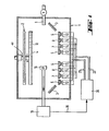
- the device represented in FIG. 1 and designed for the implementation of the method according to the invention comprises a chamber under high vacuum 1, in which there are a heating plate 2 and / or two radiators 3. These heating elements 2 and 3 are used to preheat the substrate 4 to the desired temperature, and to maintain it at this temperature during the formation of the layer.
- the substrate 4 is placed on a support 10 movable in rotation about an axis 11.
- the temperature of the heating plate 2 and that of the radiators 3 are regulated by means of a thermoelectric device as a function of the surface temperature of the substrate. 4. In order not to overload the figure, the temperature control devices are not shown.
- the device further comprises a gas metering system with a pipe 9 for supplying gas into the enclosure 1.
- the 0n preheats the semiconductor in the evaporation crucible 5 on the one hand, and the dopant in the evaporation crucible 6 on the other hand, to the temperature necessary for evaporation thanks to the heating elements 12 and 13 respectively electric. It is also possi ble to use as heating elements 12 and 13 electron guns which direct the electron beam directly on the material to be evaporated. Furthermore, the electric heating element 14 serves to bring the material which will form the anti-reflection layer to the evaporation temperature.
- the probe 16 of a mass spectrometer 18 is made to enter the enclosure 1, by means of which the composition of the vapor phase is continuously measured during the deposition.
- the digital values communicated by the mass spectrometer 18 are transmitted to the regulator 20 by the electrical connection 19.
- the regulator 20 independently controls the heating elements 12 and 13 by the connection 21 according to the values which give it are transmitted, so that it is possible to modify not only the overall rate of evaporation, but also that of one or the other of the materials contained in the crucibles 5 or 6.
- By the connection 23 one controls l 'heating element 14 which allows to bring to their evaporation temperature the materials contained in the crucibles 7 and 8 and intended to form the anti-reflection layer.
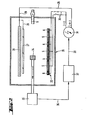
- the device also shown schematically in Figure 2 is designed to implement the method according to the invention by sputtering.
- the heating plate 26 disposed inside the high vacuum enclosure 25, and which makes it possible to bring the substrate 27 to the temperature suitable for depositing the layers also acts as an anode and is connected by the wire 28 to the positive pole of a high-voltage generator 30.
- the substrate 27 itself acts directly as an anode via the wire 29.
- the cathode is constituted by the plate 32 which is connected to the negative pole of the high voltage generator 30 by wire 33.
- the constituent elements of the layer, namely the semiconductor 5 and the dopant 6 are placed on this cathode 32 in the appropriate state.
- the gas line 9 is as previously connected to a gas metering device and is used to fill the enclosure 25 with a suitable gas, for example necessary for the performance of an annealing operation after deposition.
- a piezoelectric quartz 34 on which a layer is deposited as on the substrate 27. Due to the growth of a semiconductor layer on its surface, the quartz 34 sees its resonant frequency to modify ; it is thus possible to continuously measure the growth rate of the semiconductor layer according to the drift of the resonance frequency of the quartz.
- the processing of the signals takes place in the analyzer 35, which controls the regulator 37 by the connection 36.
- the regulator 37 controls the high-frequency generator 30 itself by means of the connection 38, the output voltage of the generator being adjusted in such a way so that it displays a value suitable for the desired growth rate of the semiconductor layer on the substrate.
- FIG. 2 represents only a single piezoelectric quartz supplemented with measuring and adjusting apparatuses
- the invention can also be executed in a particularly advantageous form with two piezoelectric quartzes and the corresponding measuring and adjusting apparatuses.
- the two quartz and the corresponding devices relate respectively to the sputtering speed of the semiconductor and that of the dopant. In this way, the quantities of each component can be measured separately, and the corresponding spraying rates adjusted separately.
- the substrate is a sheet metal plate 4 made of chrome-vanadium steel (115 Cr V 3). Before introducing it into enclosure 1, the face on which the deposit will be made is thoroughly cleaned. Then it is fixed on the pivoting support 10.
- the semiconductor used is germanium, and the dopant aluminum, in a germanium / aluminum weight ratio of 4.3 / 1.
- the two elements are introduced separately into tungsten crucibles 5 and 6 and the crucibles are placed at a distance of approximately 20 cm from the face of the substrate to be covered, above the individually adjustable heating elements 12 and 13.
- the chamber 1 Maintained the chamber 1 under a residual pressure of 3.10- 5 mbar during evaporation. Thanks to the heating plates 2 and / or to the radiator 3, the substrate is brought to 290 ° C. and it is regulated at this temperature by interposed thermocouples. It is then that the support 10 is rotated. The heating elements 12 and 13 are then connected, giving them a power such that a semiconductor layer is formed on the substrate 5 at a speed of 30 nanometers per second. After 30 seconds, the electrical supply to the heating elements 12 and 13 is cut off. A layer 295 nanometers thick is then formed.
- the growth rate of the layer is measured using the mass spectrometer 16, 18.
- the mass of the germanium isotope 72 is first measured as well as that of the aluminum isotope 27 corresponding to the desired growth rate of 30 nanometers per second and this value is programmed in the spectrometer 18.
- the spectrometer 18 controls the regulator 20 so that the respective amounts of germanium and aluminum previously programmed in the spectrometer are always respected. Therefore, the two materials are applied to the substrate 4, heated accordingly, in the proportions previously determined.
- the heating plate 2 and the radiators 3 are disconnected. Then, when the substrate 4 has practically reached room temperature, the heating element 14 is connected with the aid of which it is evaporated.
- the quantities of cerium oxide (Ce0 2 ) are chosen in such a way that, after complete evaporation, an anti-reflection layer of 0.063 ⁇ m thick has formed. about.
- the substrate coated with the layers formed according to the invention is annealed, in enclosure 1, for one hour, at a temperature of 250 ° C. under vacuum.
- the enclosure 1 is then aerated and the substrate is removed therefrom.
- FIG. 3 illustrates the spectrophotometric properties of the layer obtained.
- Curve 40 represents the absorption factor A
- curve 41 the reflection factor R of the layer, as a function of the wavelength. It can be seen that, up to a wavelength of approximately 1 ⁇ m, approximately 95% of the radiation is absorbed, and this value drops suddenly, between 1 and 3 ⁇ m to reach 10%. On the contrary, the reflective power of the layer which is only about 5% below 1 ⁇ m rises suddenly between 1 and 3 ⁇ m to reach around 90%.
- this layer largely fulfills the following conditions which are those of the ideal functioning of an absorber of solar radiation by photothermal effect: absorbing as much as possible the solar radiation which falls on the surface of the earth after being modified by the crossing of the atmosphere, and whose maximum energy corresponds in the spectrum to a wavelength of 0.55 ⁇ m, and on the other hand prevent that the energy absorbed by the layer is not lost due to of a clean emission in the long wavelengths following a rise in temperature.
- curves 42 and 43 illustrate the effectiveness of the layer according to the invention.
- the layer 42 represents, still as a function of the wavelength, the energy distribution of the direct solar radiation, and the layer 43 the energy distribution of the thermal radiation emitted by a wall whose temperature is 300 ° C. Since precisely in the long wavelength range where the thermal radiation of the wall is important, the reflection factor of the layer is very high, then the radiation losses are reduced to a minimum, because it is well known that 'A high reflecting power corresponds to a low emissivity.
- FIG. 4 represents a diagram in which the layer 44 and the curve 45 express, as a function of the working temperature of the absorber, for a radiated solar energy of 1 kW / m 2 , on the one hand the yield of an absorbent layer according to the invention and secondly, that of a black absorber. It can be seen that, whatever the working temperature which can be determined in a known manner from the amount of heat removed by a heat exchanger, the yield is much higher in the case of the layer according to l invention only in that of a black absorber.
- a black absorber has, at a temperature of 120 ° C, which corresponds to the maximum temperature that 'it can reach under the effect of solar radiation, and provided that it is completely freed from heat losses by conduction or convection, a practically zero efficiency.
- the diagram of FIG. 5 represents by curves 46 and 47 the evolution as a function of time of the temperature, on the one hand of an absorber according to the invention, and on the other hand of a black absorber when sets the following conditions: at time to, a Ener- gi e is provided to 1 kW / m 2, and at time t 1, it removes.
Landscapes
- Physical Vapour Deposition (AREA)
Applications Claiming Priority (2)
| Application Number | Priority Date | Filing Date | Title |
|---|---|---|---|
| DE3216387A DE3216387C2 (de) | 1982-05-03 | 1982-05-03 | Verfahren und Vorrichtung zur Herstellung einer hochdotierten Halbleiterschicht auf einem temperaturbeständigen Feststoff-Grundkörper |
| DE3216387 | 1982-05-03 |
Publications (1)
| Publication Number | Publication Date |
|---|---|
| EP0093672A2 true EP0093672A2 (de) | 1983-11-09 |
Family
ID=6162501
Family Applications (1)
| Application Number | Title | Priority Date | Filing Date |
|---|---|---|---|
| EP83400881A Withdrawn EP0093672A2 (de) | 1982-05-03 | 1983-05-03 | Aufbringen einer dotierten Halbleiterschicht auf ein Substrat um eine selektiv reflektierende Schicht zu bilden |
Country Status (3)
| Country | Link |
|---|---|
| EP (1) | EP0093672A2 (de) |
| JP (1) | JPS5936974A (de) |
| DE (1) | DE3216387C2 (de) |
Cited By (2)
| Publication number | Priority date | Publication date | Assignee | Title |
|---|---|---|---|---|
| GB2218606A (en) * | 1987-08-06 | 1989-11-22 | Stc Plc | Wavelength selective filter |
| WO2023018758A1 (en) * | 2021-08-10 | 2023-02-16 | Virginia Commonwealth University | Sputtering machines, substrate holders, and sputtering processes with magnetic biasing |
Family Cites Families (5)
| Publication number | Priority date | Publication date | Assignee | Title |
|---|---|---|---|---|
| DE623488C (de) * | ||||
| NL180750B (nl) * | 1952-08-20 | Bristol Myers Co | Werkwijze voor het bereiden van een 7-amino-3-cefem-4-carbonzuur derivaat door een 7-acylamino-3-cefem-4-carbonzuur derivaat om te zetten. | |
| GB1108741A (en) * | 1963-09-19 | 1968-04-03 | Ass Elect Ind | Improvements in and relating to epitaxial layers of semiconductor materials |
| DE1544312A1 (de) * | 1964-03-20 | 1970-07-02 | Telefunken Patent | Verfahren zum Einbauen von Fremdstoffen in einen Halbleiter oder Isolator |
| DE3027657A1 (de) * | 1980-07-22 | 1982-02-25 | Ramot University Authority for Applied Research and Industrial Development Ltd.,, Tel Aviv | Verfahren zur herstellung von halbleiter-schichten |
-
1982
- 1982-05-03 DE DE3216387A patent/DE3216387C2/de not_active Expired
-
1983
- 1983-05-03 EP EP83400881A patent/EP0093672A2/de not_active Withdrawn
- 1983-05-04 JP JP58077655A patent/JPS5936974A/ja active Pending
Cited By (3)
| Publication number | Priority date | Publication date | Assignee | Title |
|---|---|---|---|---|
| GB2218606A (en) * | 1987-08-06 | 1989-11-22 | Stc Plc | Wavelength selective filter |
| GB2218606B (en) * | 1987-08-06 | 1991-01-30 | Stc Plc | Wavelength selective filter |
| WO2023018758A1 (en) * | 2021-08-10 | 2023-02-16 | Virginia Commonwealth University | Sputtering machines, substrate holders, and sputtering processes with magnetic biasing |
Also Published As
| Publication number | Publication date |
|---|---|
| DE3216387A1 (de) | 1983-11-03 |
| JPS5936974A (ja) | 1984-02-29 |
| DE3216387C2 (de) | 1985-09-19 |
Similar Documents
| Publication | Publication Date | Title |
|---|---|---|
| US5725671A (en) | Apparatus for manufacturing chalcopyrite film | |
| US5667597A (en) | Polycrystalline silicon semiconductor having an amorphous silicon buffer layer | |
| EP0853345B1 (de) | Verfahren zur herstellung einer cdte-schicht | |
| EP2976577B1 (de) | Absorbierendes material und solarpaneel mit einem derartigen material | |
| US5500102A (en) | Method of forming deposited semiconductor film | |
| EP3596408B1 (de) | Mehrschichtiges material | |
| WO2011111029A1 (fr) | Procede de traitement d'un contact metallique realise sur un substrat | |
| EP0045551A1 (de) | Verfahren zur Herstellung polykristalliner Filme aus Halbleitern, die aus einer Verbindung oder einem Element bestehen, und dabei erhaltene Filme | |
| Feldman et al. | Evaporated polycrystalline silicon films for photovoltaic applications-grain size effects | |
| US5427817A (en) | Process for manufacturing an auto-collimating scintillator and product produced thereby | |
| FR2827707A1 (fr) | Procede de realisation d'un detecteur bolometrique et detecteur realise selon ce procede | |
| Abd El-Mongy et al. | A comparison of the physical properties of CdTe single crystal and thin film | |
| FR2732697A1 (fr) | Couches minces d'alliages quasi-cristallins, leur preparation et leurs utilisations | |
| FR2465319A1 (fr) | Cellule photovoltaique | |
| Garnich et al. | Cu SiO2/Cu-cermet selective absorbers for solar photothermal conversion | |
| WO2009133315A2 (fr) | Procede de fabrication d'une cellule photovoltaïque a base de silicium en couches minces | |
| EP1007754B1 (de) | Aufdampfung von dünnen filmen bei schiefen einfall winkeln | |
| EP3640366A1 (de) | Herstellungsverfahren eines mehrschichtigen wärmeregulierten materials auf vo2-basis | |
| Kolodzey et al. | Properties of a‐Si, Ge: H, F alloys prepared by rf glow discharge in an ultrahigh vacuum reactor | |
| FR3072212B1 (fr) | Dispositif electrique a transition entre des comportements isolant et semiconducteur | |
| LU82690A1 (fr) | Procede de preparation de films polycristallins semiconducteurs composes ou elementaires et films ainsi obtenus | |
| JP2000357808A (ja) | シリコン系薄膜光電変換装置およびその製造方法 | |
| Pandey et al. | Influence of Thermal Annealing on Structural and Optical Properties of Sb Doped ZnTe Thin Film | |
| Ortiz et al. | Lithium doped zinc oxide photoluminescence films prepared by spray pyrolysis | |
| Claudio et al. | Optical characterisation of aluminium nitride as antireflective coating by a new remote plasma deposition system |
Legal Events
| Date | Code | Title | Description |
|---|---|---|---|
| PUAI | Public reference made under article 153(3) epc to a published international application that has entered the european phase |
Free format text: ORIGINAL CODE: 0009012 |
|
| AK | Designated contracting states |
Designated state(s): AT BE CH DE FR GB IT LI LU NL SE |
|
| STAA | Information on the status of an ep patent application or granted ep patent |
Free format text: STATUS: THE APPLICATION IS DEEMED TO BE WITHDRAWN |
|
| 18D | Application deemed to be withdrawn |
Effective date: 19860310 |
|
| R18D | Application deemed to be withdrawn (corrected) |
Effective date: 19860310 |
|
| RIN1 | Information on inventor provided before grant (corrected) |
Inventor name: KESSLER, FRANZ RUDOLF Inventor name: RITTERS, ERNST-WILHELM Inventor name: DETTMER, KLAUS |