EP0093954A2 - Bildanzeigespeicher - Google Patents
Bildanzeigespeicher Download PDFInfo
- Publication number
- EP0093954A2 EP0093954A2 EP83104112A EP83104112A EP0093954A2 EP 0093954 A2 EP0093954 A2 EP 0093954A2 EP 83104112 A EP83104112 A EP 83104112A EP 83104112 A EP83104112 A EP 83104112A EP 0093954 A2 EP0093954 A2 EP 0093954A2
- Authority
- EP
- European Patent Office
- Prior art keywords
- display memory
- display
- data
- memories
- dot
- Prior art date
- Legal status (The legal status is an assumption and is not a legal conclusion. Google has not performed a legal analysis and makes no representation as to the accuracy of the status listed.)
- Withdrawn
Links
- 230000015654 memory Effects 0.000 title claims abstract description 108
- 238000004040 coloring Methods 0.000 abstract description 14
- 238000010586 diagram Methods 0.000 description 10
- 239000003086 colorant Substances 0.000 description 6
- 238000012545 processing Methods 0.000 description 6
- 230000002146 bilateral effect Effects 0.000 description 4
- 230000002093 peripheral effect Effects 0.000 description 3
- 230000002776 aggregation Effects 0.000 description 1
- 238000004220 aggregation Methods 0.000 description 1
- 238000013479 data entry Methods 0.000 description 1
- 230000000717 retained effect Effects 0.000 description 1
Images



Classifications
-
- G—PHYSICS
- G09—EDUCATION; CRYPTOGRAPHY; DISPLAY; ADVERTISING; SEALS
- G09G—ARRANGEMENTS OR CIRCUITS FOR CONTROL OF INDICATING DEVICES USING STATIC MEANS TO PRESENT VARIABLE INFORMATION
- G09G5/00—Control arrangements or circuits for visual indicators common to cathode-ray tube indicators and other visual indicators
- G09G5/02—Control arrangements or circuits for visual indicators common to cathode-ray tube indicators and other visual indicators characterised by the way in which colour is displayed
- G09G5/022—Control arrangements or circuits for visual indicators common to cathode-ray tube indicators and other visual indicators characterised by the way in which colour is displayed using memory planes
Definitions
- the present invention relates to an image display device capable of displaying color image at a high resolution.
- Fig. 1 shows a display screen of such a dot-by-dot coloring display device and a graphic pattern displayed on the display screen.
- Fig. 2 diagramatically shows contents of data written in three R. G and B display memories for three principal colors when the graphic pattern shown in Fig. 1 is displayed on the display screen with dot-by-dot coloring.
- the dot-by-dot coloring graphic display is now explained with reference to Figs. 1 and 2.
- the graphic pattern shown in Fig. 1 illustrates straight lines shown by solid lines A 1 - A 4 and crossing straight lines shown by broken lines B 1 - B 4 , and the respective lines are colored as shown in Fig. 2.
- the addresses of the display memory are assigned n bytes (n x 8 bits) in horizontal line of the display screen shown in Fig. 1 and the addresses are sequentially increased starting from left top and ending at right bottom (0, 1, ---- n-1, n, n+1, ----) as shown in Fig. 2.
- any different coloring of 8-bit brightness information of the same address in the display memory is required as shown in Fig. 2 (for example, at address 0 in Fig. 2).
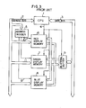
- Fig. 3 shows a block diagram of a display memory unit having three R, G and B display memories for attaining the dot-by-dot coloring.
- numeral 1 denotes a CPU
- numeral 2 denotes an address bus
- numeral 3 denotes a data bus
- numeral 4 denotes a read/write selection signalline
- numeral 5 denotes an address decoder
- numerals 6, 7 and 8 denote display memories for three principal colors (R, G and B)
- numeral 9 denotes a bilateral buffer
- numerals 10, 11 and 12 denote selection signal lines by which the CPU 1 accesses the display memories 6, 7 and 8, respectively.
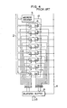
- Fig. 4 shows a detailed circuit diagram of the display memory 6 shown in Fig. 3.
- the display memories 7 and 8 are similar to that shown in Fig. 4.
- the display memory 6 has the same number of memory positions as the number of bits of the data bus, that is, eight in the illustrated example, which are connected to the data bus 3 through the bilateral buffer 9. The writing of the intensity information into the display memories in Figs. 3 and 4 is now explained.
- the CPU 1 determines that graphic figures written into the display memory 6 are coloring designations including "red" of the three principal colors, it addresses the display memory 6 to write the intensity information of the graphic pattern into the red display memory 6 and sends a write address to the address bus 2.
- the address is decoded by the address decoder 5 so that only the display memory 6 is selected and enabled for writing by the selection signal 10. Since the read/write selection signal line 4 from the CPU 1 controls the bilateral buffer 9 such that the data is supplied from the CPU 1 to the display memory, the data is written into only the display memory 6 addressed by the CPU 1 although the write data is supplied to the display memories 6, 7 and 8. As shown in Fig. 2, the eight bits on the data bus 3 are written as they are. Similarly, the green and blue intensity information are written into the green and blue display memories 7 and 8, respectively, when they are addressed.
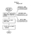
- the three R, G and B display memories are arranged in different address spaces as viewed from the CPU and the software processing for writing into the display memory as shown in Fig. 5 must be carried out three times for each writing of one graphic data. Accordingly, when the graphic pattern is to be written over the entire display screen, a very large number of processings and long time are required.
- a display memory unit having a plurality of display memories connected to data lines of a data bus one for each display memory chip and addressable for each bit of the data bus is provided, and the display memory unit includes display memory chip selection means for selecting the display memory chip for each data bit on the same address, and write control means for controlling writing for each display memory.
- the dot-by-dot coloring is attained only by the software processing of controlling the write information for each display memory and selecting the display memory chip.
- Fig. 6 shows a block diagram of one embodiment of the display memory unit of the present invention.
- numeral 13 denotes a data gate circuit which gates the data on the data bus 3 by the display memory select signal 14 from the output of the address decoder 5.
- Numeral 15 denotes a data bit selection signal for selecting a data bit of each of the display memories 6, 7 and 8 by the output of the data gate circuit 13.
- Numerals 16, 17 and 18 denote color registers for instructing writing of data into the display memories 6, 7 and 8, respectively. The output signals therefrom are supplied to data input terminals of the respective display memories.
- the data gate circuit 13 selects the display memory for each data bit to be written into the display memories 6, 7 and 8. It gates the data on the data bus 3 by the display memory selection signal 14 and supplies the output signal to the display memories 6, 7 and 8 as the bit selection signal for the respective display memories.
- the color registers 16, 17 and 18 store color information of the graphic patterns for instructing whether the graphic data to be displayed are written into the display memories 6, 7 and 8 or not.
- Fig. 7 shows a circuit diagram to illustrate the connection of the display memory 6, the data gate circuit 13 and the color register 16 shown in Fig. 6.
- the peripheral circuits of the display memories 7 and 8 are also connected in the same manner.
- the data gate circuit 13 comprises eight AND circuits and it supplies the data on the data bus 3 to the memory chips of the display memories 6, 7 and 8 as the selection signal 15, by the display memory selection signal 14 from the output of the address decoder 5.
- the color register is a one-bit latch and the output signal thereof is supplied to the display memory 6 as the data entry signal to the display memory 6.
- the writing of the data into the display memories in the display memory unit shown in Figs. 6 and 7 is now explained.
- the CPU 1 designates the colors of the graphic pattern to be displayed by three bits, one for each of R, G and B, and the color information is sotred in the color registers 16, 17 and 18.
- the intensity information of the graphic pattern to be displayed is then written at the address of the display memories corresponding to the address on the display screen.
- the address of the display memory is on the address bus 2 and the address decoder 5 produces the display memory selection signal 14 so that the data gate circuit 13 is opened.
- the intensity information to be written into the display memory is on the data bus 3, and this data is supplied to the display memories 6, 7 and 8 through the data gate circuit 13 as the memory chip selection signal 15.
- the writing of the color information of the color register is permitted for the bit of the display memory to which the "1" intensity information data is supplied, and the writing of the data is not permitted for the bit of the display memory to which the "0" data is supplied. Accordingly, as explained above in connection with Fig.
- Fig. 8 shows a flow chart of a data write software for the display memory in the present embodiment.
- the new data can be written into the three R, G and B display memories without erasing the recorded data, only by writing the color information into the color registers and the intensity information into the display memories.
- the software processing is significantly reduced to compare with that of the prior art unit in which the results of the separate logical operations are written into the three R, G and B display memories. If the color information of the graphic data does not change, the color information need not be written into the color registers every time because the color information is retained in the color registers, but it may be written only when the color information changes. Thus, the software processing time can be further reduced.
- the hardware several logic circuits for the color registers and the data gate are additionally required to compare with the prior art unit but the bilateral buffer 9 is not necessary because the contents of the display memories 6, 7 and 8 need not be read out in the present embodiment as opposed to the prior art unit shown in Figs. 3 and 4. Accordingly, the hardware scale is about the same.
- the software processing in the prior art unit in which the separate data are written into the three R, G and B display memories is not necessary and only the processing of writing the color information into the color registers and the collective writing of the intensity information into the three R, G and B display memories is required.
- the software processing is reduced.
- the software processing of writing the color information and the intensity information in a prior art so-called semi-color graphic display in which the pattern is not colored dot-by-dot but the pattern is colored byte by byte (8 bits) by a pattern memory for storing pattern information and a color memory for storing color information, can be directly applied to the present embodiment. This is a great advantage in developing softwares.
- Fig. 9 shows a circuit diagram of another embodiment of the present invention, in which the color register 16 shown in Fig. 7 is replaced by an 8-bit latch 19.
- the color can be designated for each bit of the intensity information written into the display memory.
- the graphic patterns which display the bits of the selected address with different colors such as red and blue can be simultaneously written into the display memories.
- the processing of writing the data separately to the plurality of display memories to designate the color picture cell by picture cell is not necessary but only the processing of writing the color information into the color registers for controlling the writing for each display memory and writing the intensity information into the entire display memory to select the display memory chip individually is needed. Therefore, the processing time is significantly reduced.
- the hardware scale of the present invention does not substantially increase.
Landscapes
- Engineering & Computer Science (AREA)
- Physics & Mathematics (AREA)
- Computer Hardware Design (AREA)
- General Physics & Mathematics (AREA)
- Theoretical Computer Science (AREA)
- Digital Computer Display Output (AREA)
- Controls And Circuits For Display Device (AREA)
- Image Generation (AREA)
Applications Claiming Priority (2)
| Application Number | Priority Date | Filing Date | Title |
|---|---|---|---|
| JP57070373A JPS58187996A (ja) | 1982-04-28 | 1982-04-28 | 表示メモリ回路 |
| JP70373/82 | 1982-04-28 |
Publications (2)
| Publication Number | Publication Date |
|---|---|
| EP0093954A2 true EP0093954A2 (de) | 1983-11-16 |
| EP0093954A3 EP0093954A3 (de) | 1984-10-03 |
Family
ID=13429569
Family Applications (1)
| Application Number | Title | Priority Date | Filing Date |
|---|---|---|---|
| EP83104112A Withdrawn EP0093954A3 (de) | 1982-04-28 | 1983-04-27 | Bildanzeigespeicher |
Country Status (2)
| Country | Link |
|---|---|
| EP (1) | EP0093954A3 (de) |
| JP (1) | JPS58187996A (de) |
Cited By (4)
| Publication number | Priority date | Publication date | Assignee | Title |
|---|---|---|---|---|
| US4773026A (en) * | 1983-09-26 | 1988-09-20 | Hitachi, Ltd. | Picture display memory system |
| US4821208A (en) * | 1986-06-18 | 1989-04-11 | Technology, Inc. | Display processors accommodating the description of color pixels in variable-length codes |
| GB2261803A (en) * | 1991-10-18 | 1993-05-26 | Quantel Ltd | Storing a high resolution image as several low resolution images |
| US5241658A (en) * | 1990-08-21 | 1993-08-31 | Apple Computer, Inc. | Apparatus for storing information in and deriving information from a frame buffer |
Families Citing this family (7)
| Publication number | Priority date | Publication date | Assignee | Title |
|---|---|---|---|---|
| JPS617882A (ja) * | 1984-06-21 | 1986-01-14 | 富士通テン株式会社 | 表示装置におけるビデオメモリ書込み器 |
| US4635049A (en) * | 1984-06-27 | 1987-01-06 | Tektronix, Inc. | Apparatus for presenting image information for display graphically |
| EP0481534B1 (de) * | 1984-07-23 | 1998-01-14 | Texas Instruments Incorporated | Videosystem |
| JPS6142643U (ja) * | 1984-08-24 | 1986-03-19 | 日本電気株式会社 | 複数メモリ同時更新機構 |
| JPS6162095A (ja) * | 1984-09-03 | 1986-03-29 | 富士通株式会社 | 直線表示制御装置 |
| US4742474A (en) * | 1985-04-05 | 1988-05-03 | Tektronix, Inc. | Variable access frame buffer memory |
| JPS6424565A (en) * | 1987-07-20 | 1989-01-26 | Sharp Kk | System for storing plural kinds of picture data |
Family Cites Families (1)
| Publication number | Priority date | Publication date | Assignee | Title |
|---|---|---|---|---|
| JPS559742B2 (de) * | 1974-06-20 | 1980-03-12 |
-
1982
- 1982-04-28 JP JP57070373A patent/JPS58187996A/ja active Pending
-
1983
- 1983-04-27 EP EP83104112A patent/EP0093954A3/de not_active Withdrawn
Cited By (6)
| Publication number | Priority date | Publication date | Assignee | Title |
|---|---|---|---|---|
| US4773026A (en) * | 1983-09-26 | 1988-09-20 | Hitachi, Ltd. | Picture display memory system |
| US4821208A (en) * | 1986-06-18 | 1989-04-11 | Technology, Inc. | Display processors accommodating the description of color pixels in variable-length codes |
| US5241658A (en) * | 1990-08-21 | 1993-08-31 | Apple Computer, Inc. | Apparatus for storing information in and deriving information from a frame buffer |
| GB2261803A (en) * | 1991-10-18 | 1993-05-26 | Quantel Ltd | Storing a high resolution image as several low resolution images |
| GB2261803B (en) * | 1991-10-18 | 1995-10-11 | Quantel Ltd | An image processing system |
| US5483296A (en) * | 1991-10-18 | 1996-01-09 | Quantel Limited | High resolution image storage whereby image is divided and stored as plural groups of horizontally and vertically interleavable data |
Also Published As
| Publication number | Publication date |
|---|---|
| EP0093954A3 (de) | 1984-10-03 |
| JPS58187996A (ja) | 1983-11-02 |
Similar Documents
| Publication | Publication Date | Title |
|---|---|---|
| EP0197412B1 (de) | Bildpufferspeicher mit variablem Zugriff | |
| US5241658A (en) | Apparatus for storing information in and deriving information from a frame buffer | |
| US4613852A (en) | Display apparatus | |
| US4217577A (en) | Character graphics color display system | |
| US4554538A (en) | Multi-level raster scan display system | |
| US5056041A (en) | Data processing apparatus with improved bit masking capability | |
| JPH0375873B2 (de) | ||
| US4683466A (en) | Multiple color generation on a display | |
| US5185859A (en) | Graphics processor, a graphics computer system, and a process of masking selected bits | |
| EP0231061A2 (de) | Anzeigesysteme für graphische Darstellungen | |
| US4368461A (en) | Digital data processing device | |
| US4677427A (en) | Display control circuit | |
| US5422657A (en) | Graphics memory architecture for multimode display system | |
| JPS58187996A (ja) | 表示メモリ回路 | |
| US5559533A (en) | Virtual memory hardware cusor and method | |
| EP0256838B1 (de) | System zur Verbesserung der Funktion von Zwei-Farben-Anzeigen | |
| JPS5843035A (ja) | 記憶表示装置 | |
| AU594149B2 (en) | Graphics adapter | |
| CA1233279A (en) | Color image display apparatus | |
| EP0105724B1 (de) | Dateneinschreibeinrichtung für eine graphische Farbanzeigeeinheit | |
| US4988985A (en) | Method and apparatus for a self-clearing copy mode in a frame-buffer memory | |
| JPS5919993A (ja) | キヤラクタ表示回路 | |
| JPH0352067B2 (de) | ||
| JP2774715B2 (ja) | ドットマトリクス表示装置及びそれにおける多重化表示ramへの書き込み方式 | |
| KR880000993B1 (ko) | 고정패턴용 롬 사용방법 |
Legal Events
| Date | Code | Title | Description |
|---|---|---|---|
| PUAI | Public reference made under article 153(3) epc to a published international application that has entered the european phase |
Free format text: ORIGINAL CODE: 0009012 |
|
| AK | Designated contracting states |
Designated state(s): DE GB |
|
| PUAL | Search report despatched |
Free format text: ORIGINAL CODE: 0009013 |
|
| AK | Designated contracting states |
Designated state(s): DE GB |
|
| 17P | Request for examination filed |
Effective date: 19850312 |
|
| 17Q | First examination report despatched |
Effective date: 19860321 |
|
| D17Q | First examination report despatched (deleted) | ||
| STAA | Information on the status of an ep patent application or granted ep patent |
Free format text: STATUS: THE APPLICATION HAS BEEN WITHDRAWN |
|
| 18W | Application withdrawn |
Withdrawal date: 19870615 |
|
| RIN1 | Information on inventor provided before grant (corrected) |
Inventor name: IKEDA, TETSUYA Inventor name: KOMATSU, SHIGERU Inventor name: HIRAHATA, SHIGERU Inventor name: KOYAMA, TOKUO |