EP0095618A2 - Memory system - Google Patents
Memory system Download PDFInfo
- Publication number
- EP0095618A2 EP0095618A2 EP83104667A EP83104667A EP0095618A2 EP 0095618 A2 EP0095618 A2 EP 0095618A2 EP 83104667 A EP83104667 A EP 83104667A EP 83104667 A EP83104667 A EP 83104667A EP 0095618 A2 EP0095618 A2 EP 0095618A2
- Authority
- EP
- European Patent Office
- Prior art keywords
- memory
- data
- picture
- picture data
- memory system
- Prior art date
- Legal status (The legal status is an assumption and is not a legal conclusion. Google has not performed a legal analysis and makes no representation as to the accuracy of the status listed.)
- Granted
Links
Images

Classifications
-
- G—PHYSICS
- G09—EDUCATION; CRYPTOGRAPHY; DISPLAY; ADVERTISING; SEALS
- G09G—ARRANGEMENTS OR CIRCUITS FOR CONTROL OF INDICATING DEVICES USING STATIC MEANS TO PRESENT VARIABLE INFORMATION
- G09G5/00—Control arrangements or circuits for visual indicators common to cathode-ray tube indicators and other visual indicators
- G09G5/36—Control arrangements or circuits for visual indicators common to cathode-ray tube indicators and other visual indicators characterised by the display of a graphic pattern, e.g. using an all-points-addressable [APA] memory
- G09G5/39—Control of the bit-mapped memory
- G09G5/393—Arrangements for updating the contents of the bit-mapped memory
-
- G—PHYSICS
- G09—EDUCATION; CRYPTOGRAPHY; DISPLAY; ADVERTISING; SEALS
- G09G—ARRANGEMENTS OR CIRCUITS FOR CONTROL OF INDICATING DEVICES USING STATIC MEANS TO PRESENT VARIABLE INFORMATION
- G09G5/00—Control arrangements or circuits for visual indicators common to cathode-ray tube indicators and other visual indicators
- G09G5/02—Control arrangements or circuits for visual indicators common to cathode-ray tube indicators and other visual indicators characterised by the way in which colour is displayed
- G09G5/022—Control arrangements or circuits for visual indicators common to cathode-ray tube indicators and other visual indicators characterised by the way in which colour is displayed using memory planes
Definitions
- This invention relates to a memory system which is suitable for use in combination with a color graphic display or a color printer.
- a raster scanning color graphic display system which has an IC memory of large capacity, which is compact and inexpensive.
- a color graphic display is schematically shown in Fig. 1.
- the system comprises a control device 1, a function generator 2, an external interface circuit 3, a memory control circuit 4 and three memory planes 6, 7 and 8.
- the memory planes 6, 7 and 8 are used to store data representing picture patterns of the three primary colors, i.e., red, green and blue, respectively.
- a host computer (not shown) provides an instruction through the circuit 3 that a white circle whose radius is r and whose center is (x l , y l ) be drawn.
- the control device 1 receives the data representing r and (x l , y l ) and then supplies these data to the function generator 2.
- the device 1 instructs the function generator 2 to calculate the coordinates of any point on the circle.
- the function generator 2 does this calculation and informs the control device 1 of the end of the calculation.
- the picture data representing the coordinates of points corresponding to the points on the circle to be drawn are read from the memory plane 6 and supplied to the control device 1.
- the control device 1 performs a logical operation on the data which represent the coordinates of each point on the circle and the picture data which represent the coordinates of the corresponding point and which have been read from the memory plane 6.
- the logical operation may be REPLACE operation for drawing a new picture pattern, or SET operation for changing the binary value of a data stored in the memory plane 6 to "1".
- the result of the logical operation is written into the memory plane 6.
- the sequence of operations described in the preceding paragraph are performed on the picture data stored in the other memory planes 7 and 8.
- some of the picture data stored in each memory plane, which represent the coordinates of the points on the circle to be drawn, are modified.
- the modified picture data are read from the memory planes 6, 7 and 8 by a display control circuit 9 in synchronism with display timing signals.
- a display not shown, e.g., a CRT, in the form of a white circle.
- the object of the present invention is to provide a memory system which has a plurality of memory planes each provided with an operation circuit, whereby logical operations on each of the picture data stored in each memory plane and newly input picture data are performed at the same time in specified modes and the data obtained by the operations are written into the memory planes at the same time.
- a memory system comprises a plurality of memory planes storing picture data; memory control means for controlling the writing and reading from the memory planes; and a plurality of operation means provided in one-to-one relationship with the memory planes for performing logical operations on data read from the respective memory planes.
- a control device e.g., a microprocessor
- a control device is connected to a data bus 101, an address bus 102 and a control lines 103, as is a function generator 12 and an interface circuit 13 which in turn is also connected to a host computer (not shown).
- the control device 11, the function generator 12 and the interface circuit 13 perform the same function as their respective counterparts of the known color graphic display system shown in Fig. 1 and are not therefore described in detail.
- a memory control circuit 14 is connected to the buses 101 and 102 and the line 103.
- the output of the memory control circuit 14 is coupled to bus drivers 15R, 15G and 15B through an address bus 104 and a data bus 105.
- bus drivers 15R, 15G and 15B are connected at their outputs to arithmetic logic units (ALUs) 17R, 17G and 17B through data buses 108R, 108G and 108B, respectively, and a memory planes 26, 27 and 28 through address buses 107R, 107G and 107B, respectively.
- ALUs arithmetic logic units
- Data read from the memory plane 26 are stored in a register 16R through a data bus 109R.
- Data read from the memory plane 27 are stored in a register 16G through a data bus 109G.
- Data read from the memory plane 28 are stored into a register 16B through a data bus 109B.
- the registers 16R, 16G and 16B are connected at their outputs to the ALUs 17R, 17G and 17B.
- the ALU 17R performs a logical operation on the data from the bus driver 15R and register 16R.
- the ALU 17G performs a logical operation on the data from the bus driver 16G and register 16G
- the ALU 17B performs a logical operation on the data from the bus driver 16B and register 16B.
- SN 74181 manufactured by Texas Instruments, Inc. may be used as each ALU.
- the results of operations achieved by the ALUs 17R, 17G and 17B are written into the memory planes 26, 27 and 28, respectively.
- the ALUs 17R, 17G and 17B are connected to the input of a register 18 which stores operation mode data representative of the modes of operatons.
- operation mode data may be supplied to the ALUs 17R, 17G and 17B through lines 181, 182 and 183, respectively.
- the operation mode data have been stored in the register 18 from the control device 11 through the data bus 101.
- the data, i.e., picture data, from the memory planes 26, 27 and 28 are supplied to a display control circuit 29 and displayed by a display (not shown) connected to the display control circuit 29.
- REPLACE mode REPLACE mode
- OR mode AND mode
- XOR mode SET mode
- REPLACE mode new picture pattern will be drawn, replacing the whole or part of the pattern represented by the data stored in any memory plane.
- Fig. 3A new picture pattern shown in Fig. 3A
- Fig. 3B new picture pattern shown in Fig. 3B
- Fig. 3C new picture pattern shown in Fig. 3C
- OR mode the logical sum of the picture data stored in any memory plane and the data representing a new picture pattern will be obtained.
- the memory planes 26, 27 and 28 are assigned to red pattern data, green pattern data and blue pattern data, respectively.
- the host computer (not shown) gives an instruction to the control device 11 through the interface circuit 13, thereby instructing the device 11 to a white circle be drawn.
- the circuit 13 gives this instruction to the function generator 12.
- the function generator 12 starts calculating the coordinates of any point on the circle to be drawn.
- the control device 11 selects the OR mode to thereby draw the white circle and then supplies the coordinates data from the function generator 12 to the memory control device 14 through the data bus 101.
- the control device 11 supplies address data designating the addresses of the memory planes 26, 27 and 28 to the memory control device 14 through the data bus 102.
- the memory control device 14 supplies the address data to the memory planes 26, 27 and 28 through the address bus 104, through the address bus drivers 15R, 15G and 15B and through the address buses 107R, 107G and 107B. Meanwhile, the memory control device 14 supplies the coordinate data to the ALUs 17R, 17G and 17B through the data bus 105, through the address bus drivers 15R, 15G and 15B and through the data buses 108R, 108G and 108B. Picture data are read from those addresses of the memory planes 26, 27 and 28 which are designated by the address data. These picture data are stored into the registers 16R, 16G and 16B via the data buses 109R, 109G and 109B, respectively.
- the data representing the OR mode selected by the control device 11 is supplied from the register 18 to the ALUs 17R, 17G and 17B. Also supplied to the ALUs 17R, 17G and 17B are the coordinate data representing the points on the circle to be drawn.
- the picture patterns are supplied from the registers 16R, 16G and 16B to the ALUs 17R, 17G and 17B, respectively. Therefore, the ALUs 17R, 17G and 17B simultaneously operate according to the OR mode, thereby obtaining the logical sums of the coordinate data and the picture data.
- the logical products are written into the memory planes 26, 27 and 28 at the same time.
- the data representing the OR mode is supplied from the register 18 to the ALU 17R and 17G and the data representing the AND mode is supplied from the register 18 to the ALU 17B.
Landscapes
- Engineering & Computer Science (AREA)
- Physics & Mathematics (AREA)
- Computer Hardware Design (AREA)
- General Physics & Mathematics (AREA)
- Theoretical Computer Science (AREA)
- Image Generation (AREA)
- Digital Computer Display Output (AREA)
- Controls And Circuits For Display Device (AREA)
- Dot-Matrix Printers And Others (AREA)
- Record Information Processing For Printing (AREA)
- Color, Gradation (AREA)
Abstract
Description
- This invention relates to a memory system which is suitable for use in combination with a color graphic display or a color printer.
- In recent years the memory capacity of IC memory has increased and the cost has been reduced. This has made it possible to provide a raster scanning color graphic display system which has an IC memory of large capacity, which is compact and inexpensive. Such a color graphic display is schematically shown in Fig. 1. The system comprises a control device 1, a
function generator 2, anexternal interface circuit 3, amemory control circuit 4 and threememory planes memory planes - Let us assume that a host computer (not shown) provides an instruction through the
circuit 3 that a white circle whose radius is r and whose center is (xl, yl) be drawn. The control device 1 receives the data representing r and (xl, yl) and then supplies these data to thefunction generator 2. At the same time, the device 1 instructs thefunction generator 2 to calculate the coordinates of any point on the circle. Thefunction generator 2 does this calculation and informs the control device 1 of the end of the calculation. - The picture data representing the coordinates of points corresponding to the points on the circle to be drawn are read from the
memory plane 6 and supplied to the control device 1. The control device 1 performs a logical operation on the data which represent the coordinates of each point on the circle and the picture data which represent the coordinates of the corresponding point and which have been read from thememory plane 6. The logical operation may be REPLACE operation for drawing a new picture pattern, or SET operation for changing the binary value of a data stored in thememory plane 6 to "1". The result of the logical operation is written into thememory plane 6. - The sequence of operations described in the preceding paragraph are performed on the picture data stored in the
other memory planes memory planes display control circuit 9 in synchronism with display timing signals. Thus, they are displayed by a display (not shown), e.g., a CRT, in the form of a white circle. - With the conventional display system described above, it is necessary to perform a logical operation on the data from the function generator and to write the result of the operation into each memory plane. In other words, three similar operations must be effected one after another and the results of these operation must be written into the three memory planes upon completion of the respective logical operations. Hence, the speed at which the whole system operates is inevitably low.
- The object of the present invention is to provide a memory system which has a plurality of memory planes each provided with an operation circuit, whereby logical operations on each of the picture data stored in each memory plane and newly input picture data are performed at the same time in specified modes and the data obtained by the operations are written into the memory planes at the same time.
- To achieve the object described above, a memory system according to the invention comprises a plurality of memory planes storing picture data; memory control means for controlling the writing and reading from the memory planes; and a plurality of operation means provided in one-to-one relationship with the memory planes for performing logical operations on data read from the respective memory planes.
- This invention can be more fully understood from the following detailed description when taken in conjunction with the accompanying drawings, in which:
- Fig. 1 is a block diagram of a known color graphic display system;
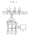
- Fig. 2 is a block diagram of one embodiment of the present invention; and
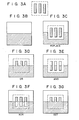
- Fig. 3 illustrates various operation modes.
- As shown in Fig. 2, a
control device 11, e.g., a microprocessor, is connected to adata bus 101, anaddress bus 102 and acontrol lines 103, as is afunction generator 12 and aninterface circuit 13 which in turn is also connected to a host computer (not shown). Thecontrol device 11, thefunction generator 12 and theinterface circuit 13 perform the same function as their respective counterparts of the known color graphic display system shown in Fig. 1 and are not therefore described in detail. Amemory control circuit 14 is connected to thebuses line 103. The output of thememory control circuit 14 is coupled tobus drivers address bus 104 and adata bus 105. - These
bus drivers data buses memory planes address buses 107R, 107G and 107B, respectively. Data read from thememory plane 26 are stored in aregister 16R through a data bus 109R. Data read from thememory plane 27 are stored in aregister 16G through a data bus 109G. Data read from thememory plane 28 are stored into aregister 16B through adata bus 109B. Theregisters ALUs bus driver 15R and register 16R. Similarly, the ALU 17G performs a logical operation on the data from thebus driver 16G and register 16G, and the ALU 17B performs a logical operation on the data from thebus driver 16B and register 16B. SN 74181 manufactured by Texas Instruments, Inc. may be used as each ALU. The results of operations achieved by theALUs memory planes ALUs register 18 which stores operation mode data representative of the modes of operatons. These operation mode data may be supplied to theALUs lines register 18 from thecontrol device 11 through thedata bus 101. The data, i.e., picture data, from thememory planes display control circuit 29 and displayed by a display (not shown) connected to thedisplay control circuit 29. - Among the operation modes represented by the data stored in the
register 18 are REPLACE mode, OR mode, AND mode, XOR mode and SET mode. When the REPLACE mode is selected, new picture pattern will be drawn, replacing the whole or part of the pattern represented by the data stored in any memory plane. For example, when an operation is conducted on a new picture pattern shown in Fig. 3A and the picture pattern shown in Fig. 3B and stored in any memory plane in the REPLACE mode, a new picture pattern shown in Fig. 3C will be drawn. When the OR mode is selected, the logical sum of the picture data stored in any memory plane and the data representing a new picture pattern will be obtained. When the AND mode is selected, the logical product of the picture data stored in any memory plane and the data representing a new picture pattern will be obtained. Similarly, when the XOR mode is selected, the exclusive logical sum of the picture data stored in any memory plane and the picture data representing a new picture pattern will be obtained. As a result, new patterns shown in Figs. 3D, 3E and 3F will be drawn when the OR mode, AND mode and XOR mode are selected. When the SET mode is selected, those of the picture data stored in any memory plane which correpond to the logic "1" data of a new picture pattern (i.e., the hatched portions) are changed to logic "1" data and those of the picture data stored in the memory plane which correspond to the logic "0" data of the new picture pattern (i.e., the blank portions) are not changed. As a result, a picture pattern shown in Fig. 3G will be drawn. - The
memory planes - How the memory system described above operates to draw a white circle having a radius of r and its center at point (xl, yl) will be described in detail.
- First, the host computer (not shown) gives an instruction to the
control device 11 through theinterface circuit 13, thereby instructing thedevice 11 to a white circle be drawn. Thecircuit 13 gives this instruction to thefunction generator 12. Thefunction generator 12 starts calculating the coordinates of any point on the circle to be drawn. Upon completion of this calculation, thecontrol device 11 selects the OR mode to thereby draw the white circle and then supplies the coordinates data from thefunction generator 12 to thememory control device 14 through thedata bus 101. Further, thecontrol device 11 supplies address data designating the addresses of thememory planes memory control device 14 through thedata bus 102. - The
memory control device 14 supplies the address data to the memory planes 26, 27 and 28 through theaddress bus 104, through theaddress bus drivers address buses 107R, 107G and 107B. Meanwhile, thememory control device 14 supplies the coordinate data to theALUs data bus 105, through theaddress bus drivers data buses registers data buses 109R, 109G and 109B, respectively. - The data representing the OR mode selected by the
control device 11 is supplied from theregister 18 to theALUs ALUs registers ALUs ALUs - To draw a yellow circle having a radius or r and its center at point (xl, yl), the data representing the OR mode is supplied from the
register 18 to theALU register 18 to theALU 17B.
Claims (9)
Applications Claiming Priority (2)
| Application Number | Priority Date | Filing Date | Title |
|---|---|---|---|
| JP57092861A JPS58209784A (en) | 1982-05-31 | 1982-05-31 | Memory system |
| JP92861/82 | 1982-05-31 |
Publications (3)
| Publication Number | Publication Date |
|---|---|
| EP0095618A2 true EP0095618A2 (en) | 1983-12-07 |
| EP0095618A3 EP0095618A3 (en) | 1987-02-25 |
| EP0095618B1 EP0095618B1 (en) | 1990-09-05 |
Family
ID=14066207
Family Applications (1)
| Application Number | Title | Priority Date | Filing Date |
|---|---|---|---|
| EP83104667A Expired EP0095618B1 (en) | 1982-05-31 | 1983-05-11 | Memory system |
Country Status (4)
| Country | Link |
|---|---|
| US (1) | US4641282A (en) |
| EP (1) | EP0095618B1 (en) |
| JP (1) | JPS58209784A (en) |
| DE (1) | DE3381857D1 (en) |
Cited By (14)
| Publication number | Priority date | Publication date | Assignee | Title |
|---|---|---|---|---|
| EP0145821A1 (en) * | 1983-12-22 | 1985-06-26 | International Business Machines Corporation | Area filling hardware for a colour graphics frame buffer |
| FR2565014A1 (en) * | 1984-05-23 | 1985-11-29 | Univ Leland Stanford Junior | QUICK MEMORY SYSTEM AND DATA PROCESSING METHOD FOR PRODUCING FRAME OF IMAGE ELEMENTS, AND QUICK MEMORY SEGMENT |
| DE3425635A1 (en) * | 1984-07-12 | 1986-01-16 | Olympia Werke Ag, 2940 Wilhelmshaven | Method for activating a raster recording device |
| EP0170977A3 (en) * | 1984-08-06 | 1988-03-16 | Honeywell Bull Inc. | Display subsystem |
| EP0184857A3 (en) * | 1984-12-14 | 1988-09-28 | Honeywell Bull Inc. | Multiple color generation on a display |
| EP0158314A3 (en) * | 1984-04-10 | 1988-11-09 | Ascii Corporation | Video display control system |
| EP0164880A3 (en) * | 1984-05-07 | 1989-05-24 | Advanced Micro Devices, Inc. | A circuit for modifying data in a display memory |
| EP0240989A3 (en) * | 1986-04-09 | 1990-01-17 | Hitachi, Ltd. | Multi-screen display control system and its method |
| EP0230352A3 (en) * | 1986-01-17 | 1990-03-07 | International Business Machines Corporation | Graphic and data display system |
| EP0240410A3 (en) * | 1986-03-31 | 1990-03-28 | Schlumberger Technologies, Inc. | Pixel processor |
| EP0201261A3 (en) * | 1985-04-30 | 1990-05-30 | International Business Machines Corporation | Processor for performing logical operations on picture element data bytes |
| US4935730A (en) * | 1984-10-16 | 1990-06-19 | Sanyo Electric Co., Ltd. | Display apparatus |
| EP0203728B1 (en) * | 1985-04-30 | 1993-09-29 | International Business Machines Corporation | Graphics picture element data byte processor |
| EP0491468A3 (en) * | 1990-11-17 | 1995-04-26 | Nintendo Co. Limited | Display range control apparatus and external storage unit for use therewith |
Families Citing this family (29)
| Publication number | Priority date | Publication date | Assignee | Title |
|---|---|---|---|---|
| JPS60216383A (en) * | 1984-04-11 | 1985-10-29 | 株式会社 アスキ− | Display controller |
| JPS60205584A (en) * | 1984-03-30 | 1985-10-17 | 横河電機株式会社 | Color graphic display unit |
| JPH0719048B2 (en) * | 1984-07-10 | 1995-03-06 | 大日本印刷株式会社 | Image processing device |
| JPS6153687A (en) * | 1984-08-24 | 1986-03-17 | 富士通株式会社 | Display controller |
| US5450342A (en) * | 1984-10-05 | 1995-09-12 | Hitachi, Ltd. | Memory device |
| US6028795A (en) | 1985-09-24 | 2000-02-22 | Hitachi, Ltd. | One chip semiconductor integrated circuit device having two modes of data write operation and bits setting operation |
| US5448519A (en) * | 1984-10-05 | 1995-09-05 | Hitachi, Ltd. | Memory device |
| US5923591A (en) * | 1985-09-24 | 1999-07-13 | Hitachi, Ltd. | Memory circuit |
| US4908779A (en) * | 1985-04-02 | 1990-03-13 | Nec Corporation | Display pattern processing apparatus |
| KR950014553B1 (en) * | 1985-05-20 | 1995-12-05 | 1995년12월05일 | Memory circuit with logic functions |
| JPS62264090A (en) * | 1986-05-12 | 1987-11-17 | ソニー株式会社 | Input interface circuit for multiscan monitor |
| US4999620A (en) * | 1986-08-21 | 1991-03-12 | Ascii Corporation | Apparatus for storing and accessing image data to be displayed on a display unit |
| JPS63167393A (en) * | 1986-12-29 | 1988-07-11 | 横河電機株式会社 | Crt display device |
| US4929933A (en) * | 1987-07-30 | 1990-05-29 | Zenith Electronics Corporations | Digital color video monitor |
| JPH01145777A (en) * | 1987-12-01 | 1989-06-07 | Pfu Ltd | Image data transfer method |
| US5068644A (en) * | 1988-05-17 | 1991-11-26 | Apple Computer, Inc. | Color graphics system |
| JPH01124895A (en) * | 1988-09-28 | 1989-05-17 | Hitachi Ltd | Access apparatus for image memory |
| JPH0648437B2 (en) * | 1988-09-28 | 1994-06-22 | 株式会社日立製作所 | Image memory access device and color image display device using the same |
| US4958146A (en) * | 1988-10-14 | 1990-09-18 | Sun Microsystems, Inc. | Multiplexor implementation for raster operations including foreground and background colors |
| US4953104A (en) * | 1989-05-18 | 1990-08-28 | Eastman Kodak Company | Page buffer for an electronic gray-scale color printer |
| US5546105A (en) * | 1991-07-19 | 1996-08-13 | Apple Computer, Inc. | Graphic system for displaying images in gray-scale |
| US5303200A (en) * | 1992-07-02 | 1994-04-12 | The Boeing Company | N-dimensional multi-port memory |
| JPH0761050A (en) * | 1993-08-28 | 1995-03-07 | Nec Corp | Multicolor printing data processing apparatus |
| US6911916B1 (en) * | 1996-06-24 | 2005-06-28 | The Cleveland Clinic Foundation | Method and apparatus for accessing medical data over a network |
| US9483959B2 (en) | 2008-08-21 | 2016-11-01 | Lincoln Global, Inc. | Welding simulator |
| US9196169B2 (en) | 2008-08-21 | 2015-11-24 | Lincoln Global, Inc. | Importing and analyzing external data using a virtual reality welding system |
| US8569655B2 (en) | 2009-10-13 | 2013-10-29 | Lincoln Global, Inc. | Welding helmet with integral user interface |
| US10913125B2 (en) | 2016-11-07 | 2021-02-09 | Lincoln Global, Inc. | Welding system providing visual and audio cues to a welding helmet with a display |
| US20180130226A1 (en) | 2016-11-07 | 2018-05-10 | Lincoln Global, Inc. | System and method for calibrating a welding trainer |
Family Cites Families (6)
| Publication number | Priority date | Publication date | Assignee | Title |
|---|---|---|---|---|
| US3473160A (en) * | 1966-10-10 | 1969-10-14 | Stanford Research Inst | Electronically controlled microelectronic cellular logic array |
| JPS559742B2 (en) * | 1974-06-20 | 1980-03-12 | ||
| US4092728A (en) * | 1976-11-29 | 1978-05-30 | Rca Corporation | Parallel access memory system |
| US4149184A (en) * | 1977-12-02 | 1979-04-10 | International Business Machines Corporation | Multi-color video display systems using more than one signal source |
| FR2465281A1 (en) * | 1979-09-12 | 1981-03-20 | Telediffusion Fse | DEVICE FOR DIGITAL TRANSMISSION AND DISPLAY OF GRAPHICS AND / OR CHARACTERS ON A SCREEN |
| DE3014437C2 (en) * | 1980-04-10 | 1982-05-27 | Siemens AG, 1000 Berlin und 8000 München | Arrangement for displaying alphanumeric characters on a screen of a display unit |
-
1982
- 1982-05-31 JP JP57092861A patent/JPS58209784A/en active Pending
-
1983
- 1983-05-11 EP EP83104667A patent/EP0095618B1/en not_active Expired
- 1983-05-11 DE DE8383104667T patent/DE3381857D1/en not_active Expired - Lifetime
- 1983-05-24 US US06/497,676 patent/US4641282A/en not_active Expired - Lifetime
Cited By (16)
| Publication number | Priority date | Publication date | Assignee | Title |
|---|---|---|---|---|
| EP0145821A1 (en) * | 1983-12-22 | 1985-06-26 | International Business Machines Corporation | Area filling hardware for a colour graphics frame buffer |
| US4745575A (en) * | 1983-12-22 | 1988-05-17 | International Business Machines Corporation | Area filling hardware for a color graphics frame buffer |
| EP0158314A3 (en) * | 1984-04-10 | 1988-11-09 | Ascii Corporation | Video display control system |
| US4897636A (en) * | 1984-04-10 | 1990-01-30 | Ascii Corporation | Video display control system for moving display images |
| EP0164880A3 (en) * | 1984-05-07 | 1989-05-24 | Advanced Micro Devices, Inc. | A circuit for modifying data in a display memory |
| FR2565014A1 (en) * | 1984-05-23 | 1985-11-29 | Univ Leland Stanford Junior | QUICK MEMORY SYSTEM AND DATA PROCESSING METHOD FOR PRODUCING FRAME OF IMAGE ELEMENTS, AND QUICK MEMORY SEGMENT |
| DE3425635A1 (en) * | 1984-07-12 | 1986-01-16 | Olympia Werke Ag, 2940 Wilhelmshaven | Method for activating a raster recording device |
| EP0170977A3 (en) * | 1984-08-06 | 1988-03-16 | Honeywell Bull Inc. | Display subsystem |
| US4935730A (en) * | 1984-10-16 | 1990-06-19 | Sanyo Electric Co., Ltd. | Display apparatus |
| EP0184857A3 (en) * | 1984-12-14 | 1988-09-28 | Honeywell Bull Inc. | Multiple color generation on a display |
| EP0201261A3 (en) * | 1985-04-30 | 1990-05-30 | International Business Machines Corporation | Processor for performing logical operations on picture element data bytes |
| EP0203728B1 (en) * | 1985-04-30 | 1993-09-29 | International Business Machines Corporation | Graphics picture element data byte processor |
| EP0230352A3 (en) * | 1986-01-17 | 1990-03-07 | International Business Machines Corporation | Graphic and data display system |
| EP0240410A3 (en) * | 1986-03-31 | 1990-03-28 | Schlumberger Technologies, Inc. | Pixel processor |
| EP0240989A3 (en) * | 1986-04-09 | 1990-01-17 | Hitachi, Ltd. | Multi-screen display control system and its method |
| EP0491468A3 (en) * | 1990-11-17 | 1995-04-26 | Nintendo Co. Limited | Display range control apparatus and external storage unit for use therewith |
Also Published As
| Publication number | Publication date |
|---|---|
| JPS58209784A (en) | 1983-12-06 |
| DE3381857D1 (en) | 1990-10-11 |
| US4641282A (en) | 1987-02-03 |
| EP0095618A3 (en) | 1987-02-25 |
| EP0095618B1 (en) | 1990-09-05 |
Similar Documents
| Publication | Publication Date | Title |
|---|---|---|
| US4641282A (en) | Memory system | |
| US4613852A (en) | Display apparatus | |
| EP0164880B1 (en) | A circuit for modifying data in a display memory | |
| US4849747A (en) | Display data transfer control apparatus applicable for display unit | |
| US6181353B1 (en) | On-screen display device using horizontal scan line memories | |
| EP0278526B1 (en) | Graphics diplay controller having clipping function | |
| US4837564A (en) | Display control apparatus employing bit map method | |
| US5248964A (en) | Separate font and attribute display system | |
| US5313227A (en) | Graphic display system capable of cutting out partial images | |
| US4747042A (en) | Display control system | |
| US4885699A (en) | Data processing apparatus for editing, filing, and printing image data by means of visual observation of the data on a display screen | |
| JPS6146839B2 (en) | ||
| JPH0253797B2 (en) | ||
| JPS62192865A (en) | Graphic display device | |
| JP3242965B2 (en) | Display control device | |
| JPS61130991A (en) | Graphic processing method and apparatus | |
| JPS6118549Y2 (en) | ||
| EP0293698A2 (en) | Graphic controller having function of painting designated area | |
| JPH0428311B2 (en) | ||
| JPS623293A (en) | Line movement drawing apparatus | |
| JPS62102288A (en) | Bit map display unit | |
| JPS6362079A (en) | Graphic display | |
| JPS6368985A (en) | Face painting system | |
| JPS61875A (en) | Method and device for graphic processing | |
| JPS6234191A (en) | Display controller |
Legal Events
| Date | Code | Title | Description |
|---|---|---|---|
| PUAI | Public reference made under article 153(3) epc to a published international application that has entered the european phase |
Free format text: ORIGINAL CODE: 0009012 |
|
| 17P | Request for examination filed |
Effective date: 19830607 |
|
| AK | Designated contracting states |
Designated state(s): DE FR GB |
|
| RAP1 | Party data changed (applicant data changed or rights of an application transferred) |
Owner name: KABUSHIKI KAISHA TOSHIBA |
|
| PUAL | Search report despatched |
Free format text: ORIGINAL CODE: 0009013 |
|
| AK | Designated contracting states |
Kind code of ref document: A3 Designated state(s): DE FR GB |
|
| 17Q | First examination report despatched |
Effective date: 19881220 |
|
| GRAA | (expected) grant |
Free format text: ORIGINAL CODE: 0009210 |
|
| AK | Designated contracting states |
Kind code of ref document: B1 Designated state(s): DE FR GB |
|
| REF | Corresponds to: |
Ref document number: 3381857 Country of ref document: DE Date of ref document: 19901011 |
|
| ET | Fr: translation filed | ||
| PLBE | No opposition filed within time limit |
Free format text: ORIGINAL CODE: 0009261 |
|
| STAA | Information on the status of an ep patent application or granted ep patent |
Free format text: STATUS: NO OPPOSITION FILED WITHIN TIME LIMIT |
|
| 26N | No opposition filed | ||
| REG | Reference to a national code |
Ref country code: GB Ref legal event code: IF02 |
|
| PGFP | Annual fee paid to national office [announced via postgrant information from national office to epo] |
Ref country code: GB Payment date: 20020508 Year of fee payment: 20 Ref country code: FR Payment date: 20020508 Year of fee payment: 20 |
|
| PGFP | Annual fee paid to national office [announced via postgrant information from national office to epo] |
Ref country code: DE Payment date: 20020516 Year of fee payment: 20 |
|
| PG25 | Lapsed in a contracting state [announced via postgrant information from national office to epo] |
Ref country code: GB Free format text: LAPSE BECAUSE OF EXPIRATION OF PROTECTION Effective date: 20030510 |
|
| REG | Reference to a national code |
Ref country code: GB Ref legal event code: PE20 |