EP0096462A1 - Druckkopfantriebsvorrichtung - Google Patents
Druckkopfantriebsvorrichtung Download PDFInfo
- Publication number
- EP0096462A1 EP0096462A1 EP83302512A EP83302512A EP0096462A1 EP 0096462 A1 EP0096462 A1 EP 0096462A1 EP 83302512 A EP83302512 A EP 83302512A EP 83302512 A EP83302512 A EP 83302512A EP 0096462 A1 EP0096462 A1 EP 0096462A1
- Authority
- EP
- European Patent Office
- Prior art keywords
- driving
- signal
- printing head
- power source
- pulse
- Prior art date
- Legal status (The legal status is an assumption and is not a legal conclusion. Google has not performed a legal analysis and makes no representation as to the accuracy of the status listed.)
- Granted
Links
- 238000001514 detection method Methods 0.000 claims abstract 5
- 230000004069 differentiation Effects 0.000 claims description 13
- 239000003990 capacitor Substances 0.000 claims description 11
- 230000003111 delayed effect Effects 0.000 claims description 3
- 230000001960 triggered effect Effects 0.000 claims description 3
- 230000001360 synchronised effect Effects 0.000 claims description 2
- 230000005284 excitation Effects 0.000 description 18
- 238000010586 diagram Methods 0.000 description 5
- 230000020169 heat generation Effects 0.000 description 4
- 239000000758 substrate Substances 0.000 description 3
- 230000000087 stabilizing effect Effects 0.000 description 2
- PNEYBMLMFCGWSK-UHFFFAOYSA-N Alumina Chemical compound [O-2].[O-2].[O-2].[Al+3].[Al+3] PNEYBMLMFCGWSK-UHFFFAOYSA-N 0.000 description 1
- 229910010293 ceramic material Inorganic materials 0.000 description 1
- 230000003247 decreasing effect Effects 0.000 description 1
- 239000011810 insulating material Substances 0.000 description 1
- 230000003313 weakening effect Effects 0.000 description 1
Images


Classifications
-
- B—PERFORMING OPERATIONS; TRANSPORTING
- B41—PRINTING; LINING MACHINES; TYPEWRITERS; STAMPS
- B41J—TYPEWRITERS; SELECTIVE PRINTING MECHANISMS, i.e. MECHANISMS PRINTING OTHERWISE THAN FROM A FORME; CORRECTION OF TYPOGRAPHICAL ERRORS
- B41J2/00—Typewriters or selective printing mechanisms characterised by the printing or marking process for which they are designed
- B41J2/315—Typewriters or selective printing mechanisms characterised by the printing or marking process for which they are designed characterised by selective application of heat to a heat sensitive printing or impression-transfer material
- B41J2/32—Typewriters or selective printing mechanisms characterised by the printing or marking process for which they are designed characterised by selective application of heat to a heat sensitive printing or impression-transfer material using thermal heads
- B41J2/35—Typewriters or selective printing mechanisms characterised by the printing or marking process for which they are designed characterised by selective application of heat to a heat sensitive printing or impression-transfer material using thermal heads providing current or voltage to the thermal head
- B41J2/355—Control circuits for heating-element selection
- B41J2/36—Print density control
- B41J2/37—Print density control by compensation for variation in current
-
- B—PERFORMING OPERATIONS; TRANSPORTING
- B41—PRINTING; LINING MACHINES; TYPEWRITERS; STAMPS
- B41J—TYPEWRITERS; SELECTIVE PRINTING MECHANISMS, i.e. MECHANISMS PRINTING OTHERWISE THAN FROM A FORME; CORRECTION OF TYPOGRAPHICAL ERRORS
- B41J9/00—Hammer-impression mechanisms
- B41J9/44—Control for hammer-impression mechanisms
- B41J9/50—Control for hammer-impression mechanisms for compensating for the variations of printer drive conditions, e.g. for compensating for the variation of temperature or current supply
Definitions
- This invention relates to a printing head driving apparatus designed especially for use in an impact printer and a thermal printer.
- an impact printer is adapted to drive a printing head through a solenoid, effecting a printing operation.
- an impact printer is of such a structure that an impact wire pin 1 is mounted on an armature.
- the impact wire pin 1 is guided toward the forward end of the printing head.
- the armature 2 is attracted to a core 4, upon excitation of a solenoid coil 3.
- the printing head is driven in synchronism with the timing of the driving pulse signal (a pulse signal synchronized with a printing timing signal), as shown in Fig. 2a.
- an excitation current b flows through the coil 3, as shown in Fig. Zb, based on the timing of the driving pulse signal a to excite the solenoid.
- a printing operation is carried out by a thermal head equipped with a heat generating element.
- the thermal head is so formed that heat generating elements 5 and a signal line 7 are wire- printed on a substrate 6, as shown in Fig. 3a.
- the substrate 6 is usually made of an insulating material, such as an alumina ceramic materials and has high thermal conductivity.
- the heat generating elements 5 are arranged in one row or more on the substrate 6.
- the number of the heat generating elements 5 is so determined as to correspond to the kinds of dots, such as the number of dots constituting one character and the number of dots for covering the wide surface of a printing paper sheet.
- the thermal head is normally made of a thermal element which is formed of a resistor and generates heat upon the expenditure of electrical power.
- a printing operation is carried out by bringing a paper sheet into direct, firm contact with the heat generating elements 5 shown in Fig. 3b, or by placing a transfer film between the heat generating element 5 and the paper sheet.
- the heat generating element 5 generates heat in synchronism with a driving pulse signal, as shown in Fig. 4a.
- the heat generation timing b of the heat generating element 5 varies, according to variations in the power source voltage of the thermal printer, as shown in Fig. 4b.
- a voltage stabilizing circuit is provided in both the conventional impact printer and the thermal printer.
- Some impact printers have such an arrangement'that, for example, a current feedback circuit is provided for each solenoid.
- a printing head driving circuit, power source circuit, etc., of the impact printer and thermal printer become complicated in their arrangement, increasing the costs of the printer as a whole.
- the object of this invention is to provide a printing head driving apparatus which can stabilize the printing timing and printing pressure of a printing head with a simple circuit arrangement, even if there is variation in the power source voltage of an impact printer, thermal printer, etc.
- a pulse signal outputting means for outputting a pulse signal in synchronism with a printing head driving pulse signal, i.e., in synchsonism with a print timing pulse signal.
- the pulse signal outputting means is adapted to output the pulse signal which varies to a predetermined pulse width.
- a driving circuit of the printing head is driven in synchronism with the pulse signal output from the pulse signal outputting means.
- the pulse signal output from the pulse signal outputting means varies in its pulse width according to variations in a power source voltage.
- a driving circuit of the printing head is driven in synchronism with the pulse signal, with the result that the printing timing and printing pressure of the printing head are made substantially constant, i.e., are stabilized.
- the impact printer and thermal printer for example, obviate the necessity of providing a circuit for stabilizing the power source voltage.
- the respective printers can be made simple in their arrangement, reducing the cost of the resultant system.
- a printing head driving apparatus according to one embodiment of this invention will be explained below, with reference to Figs. 5 and 6a to 6c.
- a print timing signal dl is supplied through an input terminal 11 to an integrating circuit 12.
- the print timing signal dl is a timing pulse signal for determining the start of a printing operation of an impact printer.
- the integrating circuit 12 comprises a resistor 12a and capacitor 12b.
- the resistor 12a is connected at one end to the input terminal 11.
- the integrating circuit 12 Upon receipt of a timing signal dl, as shown in Fig. 6a, the integrating circuit 12 generates a predetermined voltage signal Vi, as shown in Fig. 6b, which has a rise start time and fall start time corresponding to a CR time constant of the resistor 12a and capacitor 12b.
- the voltage signal Vi output from the integrating circuit 12 is supplied to one input terminal, e.g., to a noninverting input terminal of a voltage comparator 13.
- the voltage comparator 13 is comprised of, e.g., an ordinary operational amplifier.
- the noninverting input terminal of the comparator is connected to a common junction of the resistor 12a and capacitor 12b in the integrating circuit 12.
- the voltage comparator 13 has the other input terminal, i.e., an inverting terminal, connected to a series circuit of resistors 15a, 15b, which in turn is connected to a power source terminal Vcc.
- a reference voltage Vr corresponding to the voltage at a junction of the resistors 15a, 15b is supplied to the inverting terminal of the comparator 13.
- the comparator 13 compares voltages Vi and Vr to deliver an output signal (a driving pulse signal) e to the driving circuit 14 of a printing head.
- the driving circuit 14 normally includes an emitter-grounded transistor 14a and a coil 14b of a solenoid.
- the driving circuit 14 has such an arrangement that the transistor 14a is driven by a drive pulse signal e output from the voltage comparator 13 to cause an excitation current to flow through the coil 14b, i.e., to cause an excitation current to be supplied from the power source terminal Vcc.
- a voltage signal Vi having the rise start time and fall start time shown in Fig. 6b is supplied to the noninverting terminal of the voltage comparator 13.
- the above-mentioned reference voltage Vr is supplied to the inverting input terminal.
- the voltage comparator 13 compares voltage Vi and reference voltage Vr to produce a pulse signal which rises when, for example, voltage Vi is higher in level than reference voltage Vr.
- a variation in the level of the power source voltage Vcc causes a variation in the level of the reference voltage Vr.
- the output pulse signal e of the voltage comparator 13 varies in its rise start time and pulse width.
- Vrl representing a reference voltage when the power source voltage Vcc falls to a level lower than normal
- the voltage signal Vi is sliced with the reference voltage Vrl, as shown in Fig. 6c, to cause the voltage comparator 13 to produce a driving pulse signal el.
- Vr2 representing a reference voltage when the power source voltage Vcc rises above the normal level
- the voltage signal Vi is sliced with the reference voltage Vr2 to cause the voltage comparator to produce a driving pulse signal e2.
- the output pulse signal e of the voltage comparator 13 becomes a pulse signal el with a quick rise start time and a greater pulse width; whereas, when the power source voltage Vcc is at a level which is higher than normal, the output pulse signal e of the voltage comparator 13 becomes a pulse signal e2 with a slow rise time and a smaller pulse width.
- the voltage comparator 13 delivers the driving pulse signal e, with a rise start time and a pulse width corresponding to a variation of the power source voltage Vcc, to the driving circuit 14 of the printing head.
- the driving circuit 14 permits an excitation current, the timing of which corresponds to that of the drive pulse signal e, to flow through the coil 14b of the solenoid, causing the printing head to be driven. Therefore, when the power source voltage Vcc falls to a level which is lower than normal, the driving pulse signal el with a quick rise start time and a greater pulse width is supplied to the driving circuit 14.
- the rise time of the excitation current waveform of the coil 14b in the solenoid can be quickened by the driving pulse signal el.
- the drive pulse signal e2 By the drive pulse signal e2, the rise time of the excitation current waveform in the coil 14b of the solenoid is slowed down within the driving circuit 14, thereby positively preventing a situation wherein the printing time may be quickened when the power source voltage Vcc rises above the normal level. Since the driving pulse signal e2 has a smaller pulse width, the excitation current flows through the coil 14b of the solenoid for a relatively short period of time, thereby relatively weakening the attractive force of the solenoid. It is therefore possible to prevent the printing pressure of the printing head from being increased to an unnecessary extent.
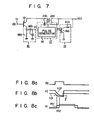
- a print timing signal d2 is supplied through an input terminal 11 to the base of a transistor 19 of a PNP type.
- the transistor 19 has its emitter supplied with a power source voltage Vcc and its collector connected to a differentiation circuit 16. With the transistor 19 ON, a power source voltage Vcc is supplied to the differentiation circuit 16.
- the differentiation circuit 16 comprised of a resistor 16a and capacitor 16b delivers a voltage signal Vj, corresponding to a CR time constant of the resistor 16a and capacitor 16b, to a monostable multivibrator 17.
- the monostable multivibrator 17 includes, for example, a pulse generator 18 and delay circuit 20 comprised of a resistor 21a and capacitor 21b, and is triggered according to the voltage signal Vj to deliver an output pulse signal (i.e., a driving pulse signal) m of a pulse width corresponding to a delay time of the delay circuit 20.
- the delay time of the delay circuit 20 is set according to the level of the power source voltage Vcc and time constant CR of the resistor 21a and capacitor 21b.
- the driving pulse signal m of the monostable multivibrator 17 is supplied to a driving circuit 14 which has the same arrangement as that shown in Fig. 5.
- the differentiation circuit 16 delivers a voltage signal Vj, as shown in Fig. 8b.
- the transistor 19 ON, the capacitor 16b in the differentiation circuit 16 is charged.
- a voltage signal Vj which is increased up to a predetermined level is supplied to the monostable multivibrator 17.
- the capacitor 16b is discharged in such a way that the voltage signal Vj begins to fall according to the CR time constant of the differentiation circuit 16.
- the power source voltage Vcc varies and reaches a high level
- the voltage signal Vj of the differentiation circuit 16 becomes voltage Vj2, as shown in Fig.
- the voltage signal Vj of the differentiation circuit 16 becomes voltage Vjl.
- the monostable multivibrator 17 is triggered into operation at a predetermined level (i.e., at the level shown in Fig. 8b) of the voltage signal Vj delivered from the differentiation circuit 16.
- the triggering timing of the monostable multivibrator varies according to voltage signals Vjl and Vj2 of the differentiation circuit 16.
- the delay time varies, due to a variation in the power source voltage Vcc, causing a variation in the pulse width of output pulse signal m of the monostable multivibrator 17.
- the pulse width of the output pulse signal ml when the power source voltage Vcc is at a lower than normal level rises to a level greater than that of an output pulse signal m2 produced when the power source voltage is at a higher than normal level.
- the monostable multivibrator 17 delivers an output pulse m, with a rise start time and pulse width corresponding to a variation of the power source voltage Vcc, to the driving circuit 14 of the printing head.
- an excitation current corresponding to the timing of the pulse signal m flows through a coil 14b in the solenoid, causing the printing head to be driven.
- a pulse signal ml with a quick pulse time is supplied to the driving circuit 14, so that the excitation current flowing through the coil of the solenoid has a quick rise time.
- the excitation current flows through the coil 14b of the solenoid over a longer period of time and it is also possible to positively prevent a lowering of the printing pressure of the printing head which might result from the attractive force of the solenoid.
- a driving pulse signal m2 With the power source voltage Vcc at a high level, a driving pulse signal m2 with a slow rise start time and a smaller pulse width is supplied to the driving circuit 14. Due to the driving pulse signal m2, the rise time of the excitation current through the coil 14b becomes slower in the driving circuit 14, positively preventing a situation wherein the printing timing is quickened, with the power source voltage Vcc being at a high level.
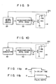
- a variation in the power source voltage Vcc is detected through a microcomputer (e.g., the microprocessor 8022 manufactured by INTEL Corporation) 30.
- the power source voltage Vcc is supplied to a microcomputer 30 through a level shift circuit 29.
- the output signal (a pulse signal) of the microcomputer 30 is supplied to a driving circuit 14 after being amplified by an operational amplifier 31.
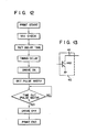
- the microcomputer 30 performs operations such as that shown in the flow chart of Fig. 12, according to a program initially stored. When a print operation starts, the print timing signal d3 shown in Fig. lla is produced within the microcomputer 30. Then, a variation of the power source voltage Vcc is detected.
- the delay time and pulse width of a driving pulse signal p is determined according to a variation of the power source voltage Vcc.
- the microcomputer 30 produces a drive pulse signal p, as shown in Fig. llb, whose rise time is delayed with reference to the timing signal d3 for the interval mentioned.
- the driving pulse signal p continues to be supplied until the period of time corresponding to the pulse width so determined has elapsed. Then, the generation of the driving pulse signal p is stopped.
- the driving pulse signal p is supplied from the computer 30 to the driving circuit 14 after being amplified through the operation amplifier 31.
- an excitation current corresponding to the timing of the driving pulse signal p flows through the coil 14b of the solenoid.
- the microcomputer 30 delivers the driving pulse signal as a pulse signal having a rise start time and pulse width corresponding to variations in the power source voltage Vcc.
- the power source voltage Vcc is, after being converted to a digital signal by an A/D converter 32, supplied to a microcomputer (e.g., microprocessor 8048, which is manufactured by INTEL Corporation) 33.
- the microcomputer 33 has a digital input/output port in which input and output signals are digital signals only.
- this embodiment has a marked advantage which is shown in Fig. 9.
- this invention has been explained as being applicable to the impact printer, it is not restricted thereto. This invention may also be applied to the thermal printer.
- a heat generating resistor 41 is provided, as shown in Fig. 13, in place of the coil 14b in the solenoid of the impact printer.
Landscapes
- Dot-Matrix Printers And Others (AREA)
- Electronic Switches (AREA)
Applications Claiming Priority (2)
| Application Number | Priority Date | Filing Date | Title |
|---|---|---|---|
| JP57080519A JPS58197063A (ja) | 1982-05-13 | 1982-05-13 | 印字ヘッド駆動方式 |
| JP80519/82 | 1982-05-13 |
Publications (2)
| Publication Number | Publication Date |
|---|---|
| EP0096462A1 true EP0096462A1 (de) | 1983-12-21 |
| EP0096462B1 EP0096462B1 (de) | 1987-02-25 |
Family
ID=13720555
Family Applications (1)
| Application Number | Title | Priority Date | Filing Date |
|---|---|---|---|
| EP83302512A Expired EP0096462B1 (de) | 1982-05-13 | 1983-05-04 | Druckkopfantriebsvorrichtung |
Country Status (5)
| Country | Link |
|---|---|
| US (1) | US4514737A (de) |
| EP (1) | EP0096462B1 (de) |
| JP (1) | JPS58197063A (de) |
| AU (1) | AU539263B2 (de) |
| CA (1) | CA1200430A (de) |
Cited By (1)
| Publication number | Priority date | Publication date | Assignee | Title |
|---|---|---|---|---|
| FR2692839A1 (fr) * | 1992-06-25 | 1993-12-31 | Sagem | Procédé d'alimentation d'une tête d'impression thermique de télécopieur et dispositif pour la mise en Óoeuvre du procédé. |
Families Citing this family (18)
| Publication number | Priority date | Publication date | Assignee | Title |
|---|---|---|---|---|
| US4706128A (en) * | 1983-12-14 | 1987-11-10 | Canon Kabushiki Kaisha | Image reading and converting apparatus |
| JPH0628335B2 (ja) * | 1984-12-27 | 1994-04-13 | 沖電気工業株式会社 | 駆動回路 |
| JPS61230962A (ja) * | 1985-04-08 | 1986-10-15 | Sato :Kk | サ−マルヘツドの温度制御装置 |
| JPS62242561A (ja) * | 1986-04-08 | 1987-10-23 | インタ−ナショナル ビジネス マシ−ンズ コ−ポレ−ション | 多重アクチユエ−タ |
| US4683817A (en) * | 1986-05-20 | 1987-08-04 | Ncr Corporation | Dot matrix print head energy control circuit |
| JPH02212164A (ja) * | 1988-10-13 | 1990-08-23 | Canon Inc | 記録方法及び装置 |
| US5053790A (en) * | 1990-07-02 | 1991-10-01 | Eastman Kodak Company | Parasitic resistance compensation for thermal printers |
| US5130720A (en) * | 1990-11-09 | 1992-07-14 | Dataproducts Corporation | System for driving ink jet transducers and method of operation |
| DE69303876T2 (de) * | 1992-10-29 | 1997-02-20 | Eastman Kodak Co | Thermo-Druckeranordnung und Betriebsverfahren |
| US5745146A (en) * | 1994-02-15 | 1998-04-28 | Monarch Marking Systems, Inc. | Dynamic strobe compensation control for a barcode printer |
| US5413423A (en) * | 1994-03-22 | 1995-05-09 | Veri Fone Inc. | Print element drive control with constant current charge and discharge of capacitor |
| US6027265A (en) * | 1997-10-14 | 2000-02-22 | Powis Parker, Inc. | Printer having improved print head mechanism and method |
| US6065884A (en) * | 1997-10-14 | 2000-05-23 | Powis Parker, Inc. | Binder strip printer and method |
| EP1027220B1 (de) * | 1997-10-14 | 2008-09-24 | Powis Parker Inc. | Ordneretikettendrucker und verfahren |
| US6755495B2 (en) * | 2001-03-15 | 2004-06-29 | Hewlett-Packard Development Company, L.P. | Integrated control of power delivery to firing resistors for printhead assembly |
| US6729707B2 (en) * | 2002-04-30 | 2004-05-04 | Hewlett-Packard Development Company, L.P. | Self-calibration of power delivery control to firing resistors |
| US6439678B1 (en) | 1999-11-23 | 2002-08-27 | Hewlett-Packard Company | Method and apparatus for non-saturated switching for firing energy control in an inkjet printer |
| US6448992B1 (en) * | 2001-11-07 | 2002-09-10 | Advanced Micro Devices, Inc. | Voltage programmable power dissipater |
Citations (4)
| Publication number | Priority date | Publication date | Assignee | Title |
|---|---|---|---|---|
| DE2360323A1 (de) * | 1972-12-26 | 1974-07-04 | Ibm | Schaltungsanordnung zur steuerung der anschlagstaerke in druckern |
| US3885469A (en) * | 1972-07-28 | 1975-05-27 | Fujitsu Ltd | Magnet operating time compensation system |
| US4027761A (en) * | 1975-10-21 | 1977-06-07 | Ncr Corporation | Matrix print head impact energy control |
| US4168421A (en) * | 1976-10-25 | 1979-09-18 | Shinshu Seiki Kabushiki Kaisha | Voltage compensating drive circuit for a thermal printer |
Family Cites Families (5)
| Publication number | Priority date | Publication date | Assignee | Title |
|---|---|---|---|---|
| JPS54156726A (en) * | 1978-05-30 | 1979-12-11 | Nippon Electric Co | Printing hammer control circuit |
| JPS5627370A (en) * | 1979-08-10 | 1981-03-17 | Canon Inc | Driving device of thermal head |
| JPS6036949B2 (ja) * | 1980-12-29 | 1985-08-23 | エプソン株式会社 | サ−マルプリンタの駆動回路 |
| JPS57128570A (en) * | 1981-02-03 | 1982-08-10 | Canon Inc | Printer |
| JPS57181882A (en) * | 1981-05-01 | 1982-11-09 | Sharp Corp | Printing density control device in thermal printer |
-
1982
- 1982-05-13 JP JP57080519A patent/JPS58197063A/ja active Pending
-
1983
- 1983-05-04 EP EP83302512A patent/EP0096462B1/de not_active Expired
- 1983-05-04 AU AU14232/83A patent/AU539263B2/en not_active Ceased
- 1983-05-10 US US06/493,275 patent/US4514737A/en not_active Expired - Fee Related
- 1983-05-11 CA CA000427926A patent/CA1200430A/en not_active Expired
Patent Citations (4)
| Publication number | Priority date | Publication date | Assignee | Title |
|---|---|---|---|---|
| US3885469A (en) * | 1972-07-28 | 1975-05-27 | Fujitsu Ltd | Magnet operating time compensation system |
| DE2360323A1 (de) * | 1972-12-26 | 1974-07-04 | Ibm | Schaltungsanordnung zur steuerung der anschlagstaerke in druckern |
| US4027761A (en) * | 1975-10-21 | 1977-06-07 | Ncr Corporation | Matrix print head impact energy control |
| US4168421A (en) * | 1976-10-25 | 1979-09-18 | Shinshu Seiki Kabushiki Kaisha | Voltage compensating drive circuit for a thermal printer |
Cited By (1)
| Publication number | Priority date | Publication date | Assignee | Title |
|---|---|---|---|---|
| FR2692839A1 (fr) * | 1992-06-25 | 1993-12-31 | Sagem | Procédé d'alimentation d'une tête d'impression thermique de télécopieur et dispositif pour la mise en Óoeuvre du procédé. |
Also Published As
| Publication number | Publication date |
|---|---|
| AU1423283A (en) | 1983-11-17 |
| EP0096462B1 (de) | 1987-02-25 |
| JPS58197063A (ja) | 1983-11-16 |
| AU539263B2 (en) | 1984-09-20 |
| US4514737A (en) | 1985-04-30 |
| CA1200430A (en) | 1986-02-11 |
Similar Documents
| Publication | Publication Date | Title |
|---|---|---|
| EP0096462A1 (de) | Druckkopfantriebsvorrichtung | |
| US4496824A (en) | Method for controlling temperature of heat generating element of thermal printing head and circuit for practising same | |
| US4741634A (en) | Printer with variable head displacement | |
| EP0913255A3 (de) | Vorrichtung und Verfahren zur Energiesteuerung für einen Thermischen Tintenstrahldruckkopf | |
| US4162131A (en) | Drive circuit for printing head | |
| US4434354A (en) | Thermal printer | |
| EP0718107B1 (de) | Wärmekopfgerät | |
| JP2000225698A (ja) | タ―ンオンエネルギの光学的測定結果からインクジェットプリンタヘッドの動作エネルギを決定する方法及び装置 | |
| EP0380352B1 (de) | Ansteuerungsschaltkreis für den Druckkopf eines Nadeldruckers | |
| US4684959A (en) | Thermal recording system using unregulated power supply | |
| US5453776A (en) | Heating element energization method for a thermal printer | |
| EP0335257B1 (de) | Punktmatrix-Anschlagdrucker | |
| US4768042A (en) | Thermosensitive gradation printer | |
| JP2554871B2 (ja) | サ−マルプリンタの印字制御装置 | |
| US5030020A (en) | Wire-dot impact printer having means for detecting displacement of individual print wires | |
| EP0272287B1 (de) | Anschlagstärkesteuerung für drucker | |
| JP3276791B2 (ja) | インクジェットヘッド駆動電源回路 | |
| JPS60165270A (ja) | サ−マルプリンタ | |
| JP2788830B2 (ja) | サーマルヘッド | |
| US4652155A (en) | Printer having a thermal head | |
| JPH0798398B2 (ja) | 印刷装置 | |
| JP2925086B2 (ja) | プリンタ装置 | |
| JPH0255150A (ja) | インパクトプリンタ | |
| JPS5957767A (ja) | 印字圧制御方式 | |
| JPS61206657A (ja) | インクジエツト記録装置 |
Legal Events
| Date | Code | Title | Description |
|---|---|---|---|
| PUAI | Public reference made under article 153(3) epc to a published international application that has entered the european phase |
Free format text: ORIGINAL CODE: 0009012 |
|
| 17P | Request for examination filed |
Effective date: 19830513 |
|
| AK | Designated contracting states |
Designated state(s): FR GB |
|
| RAP1 | Party data changed (applicant data changed or rights of an application transferred) |
Owner name: KABUSHIKI KAISHA TOSHIBA |
|
| GRAA | (expected) grant |
Free format text: ORIGINAL CODE: 0009210 |
|
| AK | Designated contracting states |
Kind code of ref document: B1 Designated state(s): FR GB |
|
| PLBE | No opposition filed within time limit |
Free format text: ORIGINAL CODE: 0009261 |
|
| STAA | Information on the status of an ep patent application or granted ep patent |
Free format text: STATUS: NO OPPOSITION FILED WITHIN TIME LIMIT |
|
| 26N | No opposition filed | ||
| PGFP | Annual fee paid to national office [announced via postgrant information from national office to epo] |
Ref country code: GB Payment date: 19920424 Year of fee payment: 10 |
|
| PGFP | Annual fee paid to national office [announced via postgrant information from national office to epo] |
Ref country code: FR Payment date: 19920511 Year of fee payment: 10 |
|
| PG25 | Lapsed in a contracting state [announced via postgrant information from national office to epo] |
Ref country code: GB Effective date: 19930504 |
|
| GBPC | Gb: european patent ceased through non-payment of renewal fee |
Effective date: 19930504 |
|
| PG25 | Lapsed in a contracting state [announced via postgrant information from national office to epo] |
Ref country code: FR Effective date: 19940131 |
|
| REG | Reference to a national code |
Ref country code: FR Ref legal event code: ST |