EP0096516B1 - Inducteur à spires multiples et circuit LC, et son procédé de fabrication - Google Patents
Inducteur à spires multiples et circuit LC, et son procédé de fabrication Download PDFInfo
- Publication number
- EP0096516B1 EP0096516B1 EP83303051A EP83303051A EP0096516B1 EP 0096516 B1 EP0096516 B1 EP 0096516B1 EP 83303051 A EP83303051 A EP 83303051A EP 83303051 A EP83303051 A EP 83303051A EP 0096516 B1 EP0096516 B1 EP 0096516B1
- Authority
- EP
- European Patent Office
- Prior art keywords
- sheet
- conductive
- laminate
- dielectric
- configuration
- Prior art date
- Legal status (The legal status is an assumption and is not a legal conclusion. Google has not performed a legal analysis and makes no representation as to the accuracy of the status listed.)
- Expired
Links
Images




Classifications
-
- H—ELECTRICITY
- H01—ELECTRIC ELEMENTS
- H01F—MAGNETS; INDUCTANCES; TRANSFORMERS; SELECTION OF MATERIALS FOR THEIR MAGNETIC PROPERTIES
- H01F41/00—Apparatus or processes specially adapted for manufacturing or assembling magnets, inductances or transformers; Apparatus or processes specially adapted for manufacturing materials characterised by their magnetic properties
- H01F41/02—Apparatus or processes specially adapted for manufacturing or assembling magnets, inductances or transformers; Apparatus or processes specially adapted for manufacturing materials characterised by their magnetic properties for manufacturing cores, coils, or magnets
- H01F41/04—Apparatus or processes specially adapted for manufacturing or assembling magnets, inductances or transformers; Apparatus or processes specially adapted for manufacturing materials characterised by their magnetic properties for manufacturing cores, coils, or magnets for manufacturing coils
- H01F41/041—Printed circuit coils
-
- H—ELECTRICITY
- H01—ELECTRIC ELEMENTS
- H01F—MAGNETS; INDUCTANCES; TRANSFORMERS; SELECTION OF MATERIALS FOR THEIR MAGNETIC PROPERTIES
- H01F41/00—Apparatus or processes specially adapted for manufacturing or assembling magnets, inductances or transformers; Apparatus or processes specially adapted for manufacturing materials characterised by their magnetic properties
- H01F41/02—Apparatus or processes specially adapted for manufacturing or assembling magnets, inductances or transformers; Apparatus or processes specially adapted for manufacturing materials characterised by their magnetic properties for manufacturing cores, coils, or magnets
- H01F41/04—Apparatus or processes specially adapted for manufacturing or assembling magnets, inductances or transformers; Apparatus or processes specially adapted for manufacturing materials characterised by their magnetic properties for manufacturing cores, coils, or magnets for manufacturing coils
-
- H—ELECTRICITY
- H01—ELECTRIC ELEMENTS
- H01F—MAGNETS; INDUCTANCES; TRANSFORMERS; SELECTION OF MATERIALS FOR THEIR MAGNETIC PROPERTIES
- H01F5/00—Coils
- H01F5/003—Printed circuit coils
-
- H—ELECTRICITY
- H03—ELECTRONIC CIRCUITRY
- H03H—IMPEDANCE NETWORKS, e.g. RESONANT CIRCUITS; RESONATORS
- H03H1/00—Constructional details of impedance networks whose electrical mode of operation is not specified or applicable to more than one type of network
- H03H2001/0021—Constructional details
- H03H2001/0085—Multilayer, e.g. LTCC, HTCC, green sheets
-
- H—ELECTRICITY
- H03—ELECTRONIC CIRCUITRY
- H03H—IMPEDANCE NETWORKS, e.g. RESONANT CIRCUITS; RESONATORS
- H03H1/00—Constructional details of impedance networks whose electrical mode of operation is not specified or applicable to more than one type of network
- H03H2001/0092—Inductor filters, i.e. inductors whose parasitic capacitance is of relevance to consider it as filter
-
- H—ELECTRICITY
- H05—ELECTRIC TECHNIQUES NOT OTHERWISE PROVIDED FOR
- H05K—PRINTED CIRCUITS; CASINGS OR CONSTRUCTIONAL DETAILS OF ELECTRIC APPARATUS; MANUFACTURE OF ASSEMBLAGES OF ELECTRICAL COMPONENTS
- H05K1/00—Printed circuits
- H05K1/16—Printed circuits incorporating printed electric components, e.g. printed resistors, capacitors or inductors
-
- H—ELECTRICITY
- H05—ELECTRIC TECHNIQUES NOT OTHERWISE PROVIDED FOR
- H05K—PRINTED CIRCUITS; CASINGS OR CONSTRUCTIONAL DETAILS OF ELECTRIC APPARATUS; MANUFACTURE OF ASSEMBLAGES OF ELECTRICAL COMPONENTS
- H05K3/00—Apparatus or processes for manufacturing printed circuits
- H05K3/10—Apparatus or processes for manufacturing printed circuits in which conductive material is applied to the insulating support in such a manner as to form the desired conductive pattern
- H05K3/20—Apparatus or processes for manufacturing printed circuits in which conductive material is applied to the insulating support in such a manner as to form the desired conductive pattern by affixing prefabricated conductor pattern
- H05K3/202—Apparatus or processes for manufacturing printed circuits in which conductive material is applied to the insulating support in such a manner as to form the desired conductive pattern by affixing prefabricated conductor pattern using self-supporting metal foil pattern
-
- Y—GENERAL TAGGING OF NEW TECHNOLOGICAL DEVELOPMENTS; GENERAL TAGGING OF CROSS-SECTIONAL TECHNOLOGIES SPANNING OVER SEVERAL SECTIONS OF THE IPC; TECHNICAL SUBJECTS COVERED BY FORMER USPC CROSS-REFERENCE ART COLLECTIONS [XRACs] AND DIGESTS
- Y10—TECHNICAL SUBJECTS COVERED BY FORMER USPC
- Y10T—TECHNICAL SUBJECTS COVERED BY FORMER US CLASSIFICATION
- Y10T156/00—Adhesive bonding and miscellaneous chemical manufacture
- Y10T156/10—Methods of surface bonding and/or assembly therefor
- Y10T156/1052—Methods of surface bonding and/or assembly therefor with cutting, punching, tearing or severing
- Y10T156/108—Flash, trim or excess removal
-
- Y—GENERAL TAGGING OF NEW TECHNOLOGICAL DEVELOPMENTS; GENERAL TAGGING OF CROSS-SECTIONAL TECHNOLOGIES SPANNING OVER SEVERAL SECTIONS OF THE IPC; TECHNICAL SUBJECTS COVERED BY FORMER USPC CROSS-REFERENCE ART COLLECTIONS [XRACs] AND DIGESTS
- Y10—TECHNICAL SUBJECTS COVERED BY FORMER USPC
- Y10T—TECHNICAL SUBJECTS COVERED BY FORMER US CLASSIFICATION
- Y10T29/00—Metal working
- Y10T29/49—Method of mechanical manufacture
- Y10T29/49002—Electrical device making
- Y10T29/4902—Electromagnet, transformer or inductor
Definitions
- LC networks inductive and capacitive networks
- these LC networks are formed by such methods as installing discrete inductors and capacitors; or by etching conductive paths in the shape of inductive coils on an insulating substrate and adding either discrete capacitors or capacitive pads on the same substrate (see for example U.S. Patent 4,021,705), both of which are labor intensive, and therefore costly. Because of the prominence of these LC networks within electrical circuits, it is highly desirable to have a low cost, and yet reliable method of manufacture for these networks.
- step of applying said second cutting means results in the removal of most of the interconnecting regions to thereby complete a multi-turn inductor, and in that the method includes the further step of
- a substantially planar, inductive-capacitive (LC) network characterized by a laminate of two pre-laminates, each of which includes a conductive sheet one surface of which is laminated to a surface of a dielectric sheet, wherein the conductive sheet of each pre-laminate has an essentially spiral-like configuration resulting in a planar multi-turn inductor in which each turn is separated from adjacent turns by a removed spiral-like configuration, and wherein the dielectric sheet of each pre-laminate contains a plurality of discontinuous apertures overlying portions of said removed spiral-like configuration of the associated conductive sheet and the remaining interconnecting portions on each dielectric sheet overlie other portions of the removed spiral-like configuration of the associated conductive sheet such that each said pre-laminate is a substantially contiguous self-supporting body without extensive gaps therein, and wherein the multi-turn inductors of each pre-laminate are positioned in general alignment with each other on opposite sides of a dielectric layer to form
- a preferred LC network may further be formed when, prior to laminating the first conductive sheet to the dielectric sheet, a similar cutting and removing operation is also performed on a second conductive sheet, resulting in a conductive path having an essentially coil-like configuration, and also having a plurality of interconnections between the adjacent windings wherein the conductive sheet remains intact.
- a preferred embodiment of the present invention is thus directed to an improved method of manufacturing LC networks and to the LC networks per se, so formed. This preferred embodiment, while involving an additional step, and hence being somewhat more costly, is particularly advantageous in that defective "short-circuited" tags are eliminated.
- Such a method thus comprises applying a cutting means, such as the male portion or punch of a zero-clearance punch and die assembly, to a first surface of a first conductive metallic sheet to cut therefrom a discontinuous predetermined pattern, forming therein a multi-turn, essentially spiral-like configuration having a plurality of interconnecting regions between adjacent turns of the spiral-like configuration.
- the remaining interconnecting regions thus add rigidity to the configured sheet. Burrs typically resulting from the cutting or punching operation extend from the surfaces of the metallic sheet opposite that at which the punch member is applied.
- a laminate is formed by laminating one surface of the configured sheet to one surface of a sheet of dielectric material.
- the dielectric sheet will be laminated to the first, i.e., burr-free, surface of the metallic sheet.
- a substantially planar, multi-turn inductor is completed by applying a second cutting means, such as the male section or punch of another zero-clearance punch and die assembly, to the laminate to remove therefrom another discontinuous predetermined pattern which includes most of the interconnecting regions between the adjacent turns in the configured metallic sheet, leaving at least one continuous portion of the spiral-like configuration with no interconnecting regions, and to cause burrs resulting from the second cutting operation to also extend from the opposite surface of the metallic sheet.
- the dielectric sheet is left with a discontinuous predetermined pattern, namely a plurality of discontinuous elongated apertures, and thus has appreciable structural integrity which provides rigidity to the laminate.
- a final laminate is formed by laminating a second conductive sheet to a dielectric layer overlying the first surface of the first metallic sheet, the second metallic sheet being aligned with the multi-turn inductor.
- the resultant sandwich of the second metallic sheet, dielectric layer, and multi-turn inductor thus forms a distributed capacitor which combines with the multi-turn inductor to provide the substantially planar LC network.
- any burrs present are directed away from the dielectric layer, and hence also away from the second metallic sheet, thus eliminating the possibility of short-circuits due to burrs extending through the dielectric layer to contact the second metallic sheet.
- the laminate formed in the second step discussed above includes the dielectric sheet laminated to the first, or burr-free, surface of the first metallic sheet
- that dielectric sheet itself may be utilized as the dielectric layer in the final laminate, such that the second metallic sheet need only be laminated to the exposed surface of the dielectric sheet.
- the second metallic sheet may be converted into a second inductor included within a second laminate by following the first three steps noted above.
- the dielectric sheet of the second laminate is also applied to the first, or burr-free, surface of the metallic sheet in the second laminate, the final laminate resulting in the LC network may be conveniently formed by fusing together the dielectric sheets of the two laminates.
- the two sheets forming the dielectric layer in the final laminate may appear to be a single sheet, resulting in a structure virtually indistinguishable from that disclosed in the earlier discussed embodiment, but in which the problem of short-circuits is avoided.
- FIG. 3 An LC network 10 according to the present invention is illustrated in Figure 3.
- This network 10 comprises a lamination having a first conductive layer 11 including a conductive path 12 which has multiple windings forming an inductor, and a second conductive layer 14 including a conductive path 15 which has multiple windings forming a second inductor.
- the conductive paths 12 and 15 are typically die cut or punched from sheets of aluminum or copper foil as will be explained.
- the multiple windings forming the conductive paths 12 and 15 consist of rectangular shaped legs which spiral inwardly in a rectangular pattern.
- the conductive layers 11 and 14 are separated by a non-conductive layer 17 therebetween.' This non-conductive layer 17 serves as a dielectric for the LC network, as will also be described.
- all three of the layers, 11, 14, and 17, forming the lamination have a configuration of voids 19 therethrough which are disposed between the adjacent windings of the conductive paths 12 and 15.
- These voids 19 are created as the result of removing certain structural interconnections 26 and 29 (see Figure 2) which exist between the conductive paths 12 and 15 prior to their lamination to the non-conductive layer 17.
- the conductive layers 11 and 14 are positioned on the non-conductive layer 17 such that at least one area 21 (see Figure 4) of the conductive path 12 is in alignment with a corresponding area 22 of the conductive path 15. This disposition or arrangement of the two conductive paths 12 and 15 with respect to each other, separated by the non-conductive layer 17 (now containing voids), introduces the capacitive element of the LC network 10.
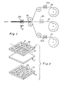
- the LC network 10 described above is manufactured by the method of the present invention, which method involves only the simple and conventional operations of die cutting and lamination and which method is adaptable to the automated manufacture of LC networks, and therefore capable of affording a reduction in the cost for these LC networks as compared to the prior art methods of manufacturing LC networks.
- the method according to the present invention utilizes a conventional die cutting press 20a, 20b, or 20c with its associated male and female dies, and conventional laminating means 23; and comprises (see Figures 1 and 2) cutting and removing a predetermined pattern from a first conductive sheet 24, leaving a conductive path 12 having an essentially coil-like configuration of windings with a plurality of interconnections 26 between the adjacent windings, wherein the conductive sheet 24 remains intact.
- a predetermined pattern may also be cut and removed from a second conductive sheet 27, leaving a conductive path 15 having an essentially coil-like configuration of windings with a plurality of interconnections 29 between the adjacent windings wherein the conductive sheet 27 remains intact.
- These conductive sheets are typically webs of metallic foils, for example aluminum or copper, which are highly conductive, and which generally have a range of thickness varying from 0.02 millimeters to 0.10 millimeters. The cutting of the conductive sheet 24 or 27 into a coil-like configuration having the interconnections 26 and 29, allows the conductive sheet to remain essentially self-supporting, i.e. tending to remain in a planar state, thus facilitating the laminating process.
- the lamination formed by the above steps is then further diecut to eliminate the interconnections 26 (and optionally 29) left between the conductive paths 12 (and 15) by the original cutting operation performed on the conductive sheet 24 (and 27), thereby completing the formulation of a multi-turn inductor within the sheet 24.
- the non-conductive sheet is cut from a web of polypropylene, which web has a thickness in the range of from 0.02 to 0.10 millimeters.
- Other non-conductive materials may be utilized providing they afford the dielectric characteristics required for capacitive elements as has been described.
- other sheet thicknesses may be utilized for the non-conductive sheet 30.
- the conductive sheets 24 and 27 Prior to laminating the conductive sheets 24 and 27 to the non-conductive sheets 30, the conductive sheets 24 and 27 are oriented such that the conductive path 12 is substantially aligned with the conductive path 15. The presence of the aligned conductive paths 12 and 15, as separated by the non-conductive sheet 30, will introduce the capacitance between the conductive sheets 24 and 27.
- FIG. 5 Another preferred method of manufacturing LC networks according to the present invention is generally illustrated in Figure 5.
- the method involves the simple and conventional operations of die cutting and laminating, which method is adaptable to the automated manufacture of LC networks and is therefore capable of purporting a reduction in the cost relative to other prior art methods.
- the method according to the present invention utilizes conventional die cutting presses with associated male and female punch and die assemblies, together with conventional laminating means.
- the first stage in this embodiment involves the formation of two separate pre-laminates 40 and 42, respectively, each of which comprises a layer of a metal sheet together with a dielectric sheet.
- a roll of a metal sheet such as a roll of aluminum foil 44. Similar materials, such as copper, having a range of thicknesses varying from 0.02 millimeters to 0.10 millimeters may also be utilized.
- the aluminum roll is then passed through a die cutting station 46, which includes a male punch member 48 and a female die member 50.
- the punch and die have a pattern such that upon application to the aluminum sheet, there is removed from the aluminum sheet a predetermined discontinuous pattern, leaving behind a conductive path having an essentially coil-like configuration containing a plurality of windings with a plurality of interconnections between the adjacent windings wherein the conductive sheet remains intact.
- the second layer of the pre-laminate 40 is. formed from a roll of dielectric material such as a roll of polyethylene 52. It will be appreciated that a large variety of various dielectric materials may similarly be utilized, such as electrical grade paper and other polymeric compositions typically utilized in electrical or capacitor applications. Where a roll of polyethylene is utilized, it may be desired to provide a primed top surface, such as by corona treatment, to enhance the adherence of the polyethylene sheet to the aluminum sheet as described hereinafter.
- the aluminum and polyethylene rolls 44 and 52, respectively, are thence brought together via a guide roller 54 and passed between pressure rollers 56 and 58, thus forming the first pre-laminate 40.
- the operation of the second punching assembly 82 removes from the pre-laminate 42 another discontinuous predetermined pattern which includes the interconnecting regions between the adjacent turns formed in the aluminum sheet 66 during the operation of the first die cutting station 70, and thus leaves within the aluminum sheet 66 of the pre-laminate 42 at least one continuous portion of the spiral-like configuration with no interconnecting regions, thereby completing another multi-turn inductor.
- burrs resulting during the operation of the second die-cutting stations 60 and 82 extend through the outward facing surfaces of the aluminum sheets.
- FIG. 6 An exploded view of the LC network provided by the method illustrated in Figure 5 is set forth in Figure 6.
- the predetermined patterns punched outwardly into the aluminum sheets 102 and 104 at the first die cutting stations 46 ad 70 shown in Figure 5 result in the formation in the aluminum sheets of a spiral-like discontinuous pattern consisting of a series of elongated apertures 106 and 108 of the aluminum sheets 102 and 104, respectively, which are separated by interconnecting regions 110 and 112, respectively.
- burrs resulting from the two stamping operations will thus project from outer facing surface of the two respective sheets and thereby face away from each other and away from any dielectric layerto be sandwiched therebetween.
- pre-laminates 40 and 42 are formed by laminating the aluminum sheets 102 and 104to the polyethylene sheets 118 and 120, respectively, as shown in Figure 6. For purposes of clarity, these respective layers are shown separated and in different stages of processing, the aluminum sheets 102 and 104 being depicted as punched by the first die cutting stations 46 and 70, while the polyethylene sheets are depicted as punched by the second die cutting stations 60 and 82.
- the multi-turn winding formed in the top aluminum layer 128 has essentially a square configuration having six turns.
- each leg of the turns has a width of approximately 1 millimeter and a space between adjacent legs of approximately 0.75 millimeter.
- the multi-turn winding formed in the bottom aluminum layer 140 is similarly dimensioned.
- the two dielectric layers, formed from the polyethylene rolls 52 and 68 shown in Figure 5, are shown in Figure 7 as a single dielectric layer 132, as the individual layers 52 and 68 having lost their individuality upon being fused together between the pressure rollers 96 and 98. Accordingly, only a dashed line representing the original boundary is shown in Figure 7.
- FIG. 8 A cross section of the resultant laminate 126, taken along the lines 8-8, is shown in Figure 8.
- the top layer 128 includes a first leg 134 of the first turn of the resultant multi-turn winding, a cut-away portion 136, a leg of the second turn 138 of the winding, an extended cutaway portion 140 representing the cut-away portion between the first and second turns, respectively, and the opposite leg 142 of the first turn.
- the bottom layer 130 includes a leg 144 of the first turn, an opening 146 between that leg ad the adjacent turn, a leg 148 of that turn, an extended cut-away portion 150 representing the removed portion between another leg of the first and second turns, and the opposite leg 152 of the first turn.
- the interlying dielectric layer 132 may also be seen to have an upper half 154 and a lower half 156, each of which is provided by the polyethylene layers 118 and 120 of Figure 6 respectively.
- the upper half 154 includes portions 158 which remain after the second cutting operation within the die cutting station 60 shown in Figure 5, and a plurality of cut-away sections 160 which were removed during the operation at the second die cutting station 60 in Figure 5.
- the portion 136 within the top layer 128 was removed from the aluminum sheet 44 during the operation of the first cutting station 46, while the portion 140 of the aluminum sheet directly above the removed portion 160 of the upper portion 154 of the dielectric layer was removed simultaneously with the removal of the portion 160 during the operation in the second cutting station 60.
- the lower portion 156 of the dielectric layer 132 includes a plurality of sections 162 interspersed by removed portions 164, which portions were removed during the operation of the second die cutting station 82.
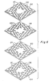
- a partial perspective view of the inductor formed within the top layer 128 and the upper portion 154 of the dielectric layer 132 is further shown in Figure 9, the leading edge of the perspective view being taken along the line 8-8 of Figure 7. It may there be seen that the leg 142 is separated from the adjoining leg 138 of the next turn by a cut-away portion 140, the next inner turn 170 being similarly separated from the second turn 138 by a cut-away portion 172. Also, the dielectric layer 154 below the cut-away portion 140 between the first and second turns may be seen to include a first portion 158 which remains, notwithstanding the removal of the overlying aluminum layer during the operation of the first cutting station 46, and a second portion 160, which was removed during the operation of the second cutting station 60. Burrs 174 provided on the edges of each of the turns of the aluminum layer 128 may further be seen in Figure 9 to extend away from the dielectric layer 154 so as to avoid any tendency to short out to the lower aluminum layer 130.
- the resultant laminate is a 5-layered construction, including two metal layers sandwiched between outer dielectric layers and an innermost dielectric layer.
- two metal rolls such as rolls of aluminum foil 176 and 178, are provided. Each roll is subjected to a first punching operation within one of the pair of punches and dies, 180 and 182, respectively.
- Each of the sets of punches and dies removes from the respective metal roll a discontinuous predetermined pattern resulting in a conductive path having an essentially spiral-like configuration and in which there are also a plurality of innerconnections between adjacent windings wherein the conductive metallic sheet remains intact, such as shown in Figure 6.
- the male, or punch, portion of the punch and die assemblies, 180 and 182 are here arranged such that any burrs resulting during the punching operation project from the outer surface of the aluminum sheets.
- the outer surface of the aluminum sheets 176, 178 are then laminated to a dielectric sheet such as provided from rolls of polyethylene 184 and 186, respectively, these rolls being coupled via guide rolls 190 and 192, to bring the polyethylene sheets into contact with the outer surface of the aluminum sheets 176 and 178 whence they are laminated together by means of sets of pressure rollers 194 and 196, in like manner to that shown in Figure 5.
- the surface of the polyethylene to be laminated to the aluminum sheets may be preferably treated such as by corona discharge to enhance the adherence to the aluminum sheet.
- the punch and die members 198 and 200 are arranged such that any burrs resulting from the second punching operations are directed outward, so as to avoid shorting out the metallic multi-turn coils once finally laminated with an interlying dielectric layer.
- a dielectric layer is included in the embodiment shown in Figure 10 by a third roll of polyethylene 207.
- the polyethylene roll 207 is brought between the two rolls of the two pre-laminates 202 and 204 via guide rolls 206, 208, 210 and 212, and the final laminate then formed by passing the combined layers between pressure rollers 214 and 216.
- the final laminate is then applied to a converter (not shown) wherein the laminate is applied to a release liner and passed through a rotary die which converts the laminate to discrete LC networks carried on a common carrier.
- dielectric materials discussed hereinabove have primarily been suggested to be formed of corona treated polyethylene webs
- similar dielectric materials typically utilized for capacitor dielectrics may be formed from webs of polypropylene having thicknesses in the range from 0.02 to 0.1 millimeter.
- Other non-conductive materials having requisite dielectric characteristics may be similarly utilized.
- the thickness of the dielectric sheets utilized in the present invention may typically be in the range of 1 to 4 mils (25-100 micrometers).
- Corona treated rolls of polyethylene are preferably provided as a coating on an underlying sheet of polyester.
- the polyester sheet is preferably removed prior to the second stamping operation, however, if desired to provide a harder surface to improve the shearing action, the polyester sheet may also be removed after the second stamping operation.
- the polyester sheet may also be removed after the second stamping operation.
- other sheet thicknesses and materials having varying dielectric constants may similarly be utilized.
- various metallic sheets may be utilized. While aluminum and copper foils may be preferred, both because of the high conductivities and low cost provided thereby, other formulations affording greater ease in punching, flexibility, or the like, may similarly be desired.
- the two planar inductors formed in the layers 102 and 104 shown in the exploded view of Figure 6 have the respective windings spiraling in opposite directions, such that, for example, the windings in inductor formed by the layer 102 spiral inwardly in a counterclockwise direction, while the windings in the lower inductor formed by the layer 104 spiral inwardly in a clockwise direction.
- the discontinuous pattern created by the first punching operations such as by the punch and die assemblies 46 and 70 in Figure 5, may be identical, a single die thus possibly being used, the second layer 104 of Figure 6 thus being provided merely by turning the second member upside down.
Landscapes
- Engineering & Computer Science (AREA)
- Power Engineering (AREA)
- Manufacturing & Machinery (AREA)
- Coils Or Transformers For Communication (AREA)
- Fixed Capacitors And Capacitor Manufacturing Machines (AREA)
- Manufacturing Cores, Coils, And Magnets (AREA)
- Filters And Equalizers (AREA)
Claims (12)
Applications Claiming Priority (2)
| Application Number | Priority Date | Filing Date | Title |
|---|---|---|---|
| US385008 | 1982-06-04 | ||
| US06/385,008 US4482874A (en) | 1982-06-04 | 1982-06-04 | Method of constructing an LC network |
Publications (2)
| Publication Number | Publication Date |
|---|---|
| EP0096516A1 EP0096516A1 (fr) | 1983-12-21 |
| EP0096516B1 true EP0096516B1 (fr) | 1987-03-11 |
Family
ID=23519658
Family Applications (1)
| Application Number | Title | Priority Date | Filing Date |
|---|---|---|---|
| EP83303051A Expired EP0096516B1 (fr) | 1982-06-04 | 1983-05-26 | Inducteur à spires multiples et circuit LC, et son procédé de fabrication |
Country Status (9)
| Country | Link |
|---|---|
| US (1) | US4482874A (fr) |
| EP (1) | EP0096516B1 (fr) |
| JP (1) | JPS592312A (fr) |
| KR (1) | KR910001642B1 (fr) |
| AU (1) | AU568076B2 (fr) |
| CA (1) | CA1200857A (fr) |
| DE (1) | DE3370233D1 (fr) |
| DK (1) | DK247683A (fr) |
| ZA (1) | ZA834053B (fr) |
Families Citing this family (28)
| Publication number | Priority date | Publication date | Assignee | Title |
|---|---|---|---|---|
| US4555291A (en) * | 1981-04-23 | 1985-11-26 | Minnesota Mining And Manufacturing Company | Method of constructing an LC network |
| DE3441328A1 (de) * | 1984-11-12 | 1986-05-15 | Siemens AG, 1000 Berlin und 8000 München | Verfahren zur herstellung von elektrischen flachspulen mit in einer flaeche liegenden windungen |
| FR2588997B1 (fr) * | 1985-10-18 | 1987-11-20 | Thomson Cgr | Procede de realisation d'une bobine de gradient et bobine obtenue par ce procede |
| US4785345A (en) * | 1986-05-08 | 1988-11-15 | American Telephone And Telegraph Co., At&T Bell Labs. | Integrated transformer structure with primary winding in substrate |
| US4846922A (en) * | 1986-09-29 | 1989-07-11 | Monarch Marking Systems, Inc. | Method of making deactivatable tags |
| US4717438A (en) * | 1986-09-29 | 1988-01-05 | Monarch Marking Systems, Inc. | Method of making tags |
| US4778552A (en) * | 1986-09-29 | 1988-10-18 | Monarch Marking Systems, Inc. | Alarm tag and method of making and deactivating it |
| CA1294117C (fr) * | 1986-09-29 | 1992-01-14 | S. Eugene Benge | Methode de fabrication d'etiquettes desactivables |
| FR2616995A1 (fr) * | 1987-06-22 | 1988-12-23 | Ebauchesfabrik Eta Ag | Procede de fabrication de modules electroniques |
| US4959631A (en) * | 1987-09-29 | 1990-09-25 | Kabushiki Kaisha Toshiba | Planar inductor |
| GB8808933D0 (en) * | 1988-04-15 | 1988-05-18 | Scient Generics Ltd | Antipilferage system |
| US4906314A (en) * | 1988-12-30 | 1990-03-06 | Micron Technology, Inc. | Process for simultaneously applying precut swatches of precured polyimide film to each semiconductor die on a wafer |
| US4926292A (en) * | 1989-08-09 | 1990-05-15 | Avantek, Inc. | Broadband printed spiral |
| US5215866A (en) * | 1989-08-09 | 1993-06-01 | Avantek, Inc. | Broadband printed spiral |
| US5321965A (en) * | 1991-11-22 | 1994-06-21 | Texas Instruments Incorporated | Inductor winding apparatus and method |
| NL9301736A (nl) * | 1993-10-08 | 1995-05-01 | Tron X B V X | Werkwijze voor het vervaardigen van een vlakke spoel, daarmee verkregen spoel, en afgestemde kring. |
| US5559487A (en) * | 1994-05-10 | 1996-09-24 | Reltec Corporation | Winding construction for use in planar magnetic devices |
| DE19650611A1 (de) * | 1996-12-06 | 1998-06-10 | Meto International Gmbh | Verfahren und Vorrichtung zur Herstellung von Sicherungselementen für die elektronische Artikelsicherung sowie ein entsprechendes Bandmaterial |
| US6988666B2 (en) * | 2001-09-17 | 2006-01-24 | Checkpoint Systems, Inc. | Security tag and process for making same |
| JP2004342755A (ja) * | 2003-05-14 | 2004-12-02 | Shinko Electric Ind Co Ltd | 平面コイルの製造方法 |
| KR100859620B1 (ko) * | 2004-10-08 | 2008-09-23 | 아세아 브라운 보베리 에스. 에이. | 전기 유도 코일 생산을 위한 반-자동 시스템 |
| JP4729464B2 (ja) * | 2006-09-20 | 2011-07-20 | ルネサスエレクトロニクス株式会社 | 方向性結合器および高周波回路モジュール |
| SE534510C2 (sv) * | 2008-11-19 | 2011-09-13 | Silex Microsystems Ab | Funktionell inkapsling |
| JP2010199291A (ja) * | 2009-02-25 | 2010-09-09 | Sae Magnetics (Hk) Ltd | コイルおよびコイル装置の製造方法 |
| WO2011027792A1 (fr) | 2009-09-01 | 2011-03-10 | 株式会社ティーアイビーシー | Procédé de fabrication d'une carte de circuits et carte de circuits |
| GB2483889A (en) | 2010-09-22 | 2012-03-28 | Tesla Engineering Ltd | Gradient coil sub assemblies |
| JP6164760B1 (ja) * | 2016-02-25 | 2017-07-19 | 株式会社放電精密加工研究所 | 螺旋状コイル製造方法 |
| US20180197676A1 (en) * | 2017-01-10 | 2018-07-12 | General Electric Company | Insulation for tranformer or inductor |
Family Cites Families (19)
| Publication number | Priority date | Publication date | Assignee | Title |
|---|---|---|---|---|
| DE1073046B (de) * | 1960-01-14 | FUBA Fabrikation funktechnischer Bauteile Hans Kolbe & Co., Bad SaIzdetfurth | Hochfrequenzanordnung für den Meter- und Dezimeterbereich, bestehend aus Induktivitäten und Kapazitäten, die als doppelseitig gedruckte Schaltungen ausgebildet sind | |
| US838423A (en) * | 1905-05-03 | 1906-12-11 | Isidor Kitsee | Method of producing electric coils. |
| FR711223A (fr) * | 1930-04-26 | 1931-09-05 | Siemens Ag | Enroulement pour bobines de transformateurs, de réactances, d'aimants, etc. |
| US2832935A (en) * | 1954-06-09 | 1958-04-29 | Aircraft Armaments Inc | Printed circuit delay line |
| US3161945A (en) * | 1958-05-21 | 1964-12-22 | Rogers Corp | Method of making a printed circuit |
| DE1156131B (de) * | 1958-06-23 | 1963-10-24 | Ibm Deutschland | Verfahren zur Herstellung eines elektrischen Leitungsmusters |
| DE1226182B (de) * | 1960-11-10 | 1966-10-06 | Siemens Ag | Verfahren zur Herstellung von sogenannten gedruckten Schaltungen mit aus Metallfoliebestehenden Leiterzuegen |
| US3301730A (en) * | 1961-04-03 | 1967-01-31 | Rogers Corp | Method of making a printed circuit |
| DE1615015B1 (de) * | 1965-01-14 | 1970-10-22 | Western Electric Co | Verfahren zur Herstellung einer gedruckten Schaltung |
| US3497410A (en) * | 1965-02-05 | 1970-02-24 | Rogers Corp | Method of die-stamping a printed metal circuit |
| US3419834A (en) * | 1966-03-24 | 1968-12-31 | Ian C. Mckechnie | Electrical coils |
| US3547724A (en) * | 1967-02-07 | 1970-12-15 | Rogers Corp | Method of and apparatus for producing printed circuits |
| BE661207A (fr) * | 1968-05-13 | 1965-07-16 | ||
| US3616039A (en) * | 1968-12-06 | 1971-10-26 | Union Carbide Corp | Method of making a laminated capacitor |
| DE6948645U (de) * | 1969-12-17 | 1970-05-14 | Saba Gmbh | Mehrkreisiges bandfilter fuer fernseh- und rundfunkempfaenger. |
| US3913219A (en) * | 1974-05-24 | 1975-10-21 | Lichtblau G J | Planar circuit fabrication process |
| US4021705A (en) * | 1975-03-24 | 1977-05-03 | Lichtblau G J | Resonant tag circuits having one or more fusible links |
| DE2714426C3 (de) * | 1977-03-31 | 1981-02-26 | Siemens Ag, 1000 Berlin Und 8000 Muenchen | Als Tiefpaß- oder als Laufzeitglied ausgebildetes passives Schaltungsglied |
| FR2412923A1 (fr) * | 1979-01-18 | 1979-07-20 | Optalix | Procede et machine pour la fabrication d'un condensateur-plan et condensateur obtenu |
-
1982
- 1982-06-04 US US06/385,008 patent/US4482874A/en not_active Expired - Lifetime
-
1983
- 1983-04-26 CA CA000426697A patent/CA1200857A/fr not_active Expired
- 1983-05-26 EP EP83303051A patent/EP0096516B1/fr not_active Expired
- 1983-05-26 DE DE8383303051T patent/DE3370233D1/de not_active Expired
- 1983-06-01 DK DK247683A patent/DK247683A/da not_active Application Discontinuation
- 1983-06-03 AU AU15363/83A patent/AU568076B2/en not_active Ceased
- 1983-06-03 ZA ZA834053A patent/ZA834053B/xx unknown
- 1983-06-03 JP JP58099268A patent/JPS592312A/ja active Granted
- 1983-06-04 KR KR1019830002500A patent/KR910001642B1/ko not_active Expired
Also Published As
| Publication number | Publication date |
|---|---|
| DK247683A (da) | 1983-12-05 |
| CA1200857A (fr) | 1986-02-18 |
| JPS592312A (ja) | 1984-01-07 |
| AU1536383A (en) | 1983-12-08 |
| KR910001642B1 (ko) | 1991-03-16 |
| US4482874A (en) | 1984-11-13 |
| AU568076B2 (en) | 1987-12-17 |
| DK247683D0 (da) | 1983-06-01 |
| ZA834053B (en) | 1984-03-28 |
| EP0096516A1 (fr) | 1983-12-21 |
| DE3370233D1 (en) | 1987-04-16 |
| JPH033925B2 (fr) | 1991-01-21 |
| KR840005301A (ko) | 1984-11-05 |
Similar Documents
| Publication | Publication Date | Title |
|---|---|---|
| US4482874A (en) | Method of constructing an LC network | |
| US4578654A (en) | Distributed capacitance lc resonant circuit | |
| US4555291A (en) | Method of constructing an LC network | |
| US4598276A (en) | Distributed capacitance LC resonant circuit | |
| EP0142380B1 (fr) | Système électronique de surveillance d'article utilisant une marque avec un circuit résonnant LC à capacitance distribuée | |
| KR100417302B1 (ko) | 적층형 코일 부품 및 그 제조방법 | |
| US4658264A (en) | Folded RF marker for electronic article surveillance systems | |
| KR960015427B1 (ko) | 적층형 코일 및 그 제조 방법 | |
| US5285191A (en) | LC marker construction useful as an electromagnetically interrogatable transponder means | |
| JPS59501030A (ja) | 物品に装着可能な荷札状片の形状をした識別装置およびその製造方法 | |
| US7008500B2 (en) | High pressure lamination of electronic cards | |
| KR20040083527A (ko) | 트랜스폰더 및 이의 제조 방법 | |
| JPH0844964A (ja) | 共振ラベル及びその製造方法 | |
| CA1200856A (fr) | Methode de fabrication de reseaux l-c | |
| US2736677A (en) | Metallized insulators | |
| US6384788B2 (en) | Antenna with a stripline feed | |
| JP2001319822A (ja) | 積層セラミック電子部品の製造方法 | |
| JP3322929B2 (ja) | 積層バンドパスフィルタ | |
| US4541559A (en) | Method of making electrical connections between opposing metal foils having a flexible, insulating layer sandwiched therebetween | |
| JPH0115160Y2 (fr) | ||
| CA2260885C (fr) | Procede de fabrication de circuits imprimes et circuit imprime fabrique selon ce procede | |
| JP2002245429A (ja) | 共振タグおよびその製造方法 | |
| EP0396524B1 (fr) | Système et méthode pour la fabrication de microplaquettes | |
| JPH10215134A (ja) | 積層emiフィルタ | |
| JP2768655B2 (ja) | チップ部品の製造方法 |
Legal Events
| Date | Code | Title | Description |
|---|---|---|---|
| PUAI | Public reference made under article 153(3) epc to a published international application that has entered the european phase |
Free format text: ORIGINAL CODE: 0009012 |
|
| AK | Designated contracting states |
Designated state(s): DE FR GB IT NL |
|
| 17P | Request for examination filed |
Effective date: 19840412 |
|
| GRAA | (expected) grant |
Free format text: ORIGINAL CODE: 0009210 |
|
| ITF | It: translation for a ep patent filed | ||
| AK | Designated contracting states |
Kind code of ref document: B1 Designated state(s): DE FR GB IT NL |
|
| REF | Corresponds to: |
Ref document number: 3370233 Country of ref document: DE Date of ref document: 19870416 |
|
| ET | Fr: translation filed | ||
| PLBE | No opposition filed within time limit |
Free format text: ORIGINAL CODE: 0009261 |
|
| STAA | Information on the status of an ep patent application or granted ep patent |
Free format text: STATUS: NO OPPOSITION FILED WITHIN TIME LIMIT |
|
| 26N | No opposition filed | ||
| REG | Reference to a national code |
Ref country code: GB Ref legal event code: 732 |
|
| PGFP | Annual fee paid to national office [announced via postgrant information from national office to epo] |
Ref country code: FR Payment date: 19910412 Year of fee payment: 9 |
|
| PGFP | Annual fee paid to national office [announced via postgrant information from national office to epo] |
Ref country code: DE Payment date: 19910423 Year of fee payment: 9 |
|
| PGFP | Annual fee paid to national office [announced via postgrant information from national office to epo] |
Ref country code: GB Payment date: 19910524 Year of fee payment: 9 |
|
| ITTA | It: last paid annual fee | ||
| PGFP | Annual fee paid to national office [announced via postgrant information from national office to epo] |
Ref country code: NL Payment date: 19910531 Year of fee payment: 9 |
|
| PG25 | Lapsed in a contracting state [announced via postgrant information from national office to epo] |
Ref country code: GB Effective date: 19920526 |
|
| PG25 | Lapsed in a contracting state [announced via postgrant information from national office to epo] |
Ref country code: NL Effective date: 19921201 |
|
| NLV4 | Nl: lapsed or anulled due to non-payment of the annual fee | ||
| GBPC | Gb: european patent ceased through non-payment of renewal fee |
Effective date: 19920526 |
|
| PG25 | Lapsed in a contracting state [announced via postgrant information from national office to epo] |
Ref country code: FR Effective date: 19930129 |
|
| PG25 | Lapsed in a contracting state [announced via postgrant information from national office to epo] |
Ref country code: DE Effective date: 19930202 |
|
| REG | Reference to a national code |
Ref country code: FR Ref legal event code: ST |