EP0096531A1 - Ein-Chip-Halbleitervorrichtung, die eine Versorgungsspannungsdetektorschaltung mit Rücksetzfunktion enthält - Google Patents
Ein-Chip-Halbleitervorrichtung, die eine Versorgungsspannungsdetektorschaltung mit Rücksetzfunktion enthält Download PDFInfo
- Publication number
- EP0096531A1 EP0096531A1 EP83303140A EP83303140A EP0096531A1 EP 0096531 A1 EP0096531 A1 EP 0096531A1 EP 83303140 A EP83303140 A EP 83303140A EP 83303140 A EP83303140 A EP 83303140A EP 0096531 A1 EP0096531 A1 EP 0096531A1
- Authority
- EP
- European Patent Office
- Prior art keywords
- power supply
- potential
- type transistor
- supply terminal
- source
- Prior art date
- Legal status (The legal status is an assumption and is not a legal conclusion. Google has not performed a legal analysis and makes no representation as to the accuracy of the status listed.)
- Granted
Links
Images








Classifications
-
- H—ELECTRICITY
- H03—ELECTRONIC CIRCUITRY
- H03K—PULSE TECHNIQUE
- H03K17/00—Electronic switching or gating, i.e. not by contact-making and –breaking
- H03K17/22—Modifications for ensuring a predetermined initial state when the supply voltage has been applied
- H03K17/223—Modifications for ensuring a predetermined initial state when the supply voltage has been applied in field-effect transistor switches
-
- G—PHYSICS
- G06—COMPUTING OR CALCULATING; COUNTING
- G06F—ELECTRIC DIGITAL DATA PROCESSING
- G06F1/00—Details not covered by groups G06F3/00 - G06F13/00 and G06F21/00
- G06F1/24—Resetting means
-
- G—PHYSICS
- G06—COMPUTING OR CALCULATING; COUNTING
- G06F—ELECTRIC DIGITAL DATA PROCESSING
- G06F1/00—Details not covered by groups G06F3/00 - G06F13/00 and G06F21/00
- G06F1/26—Power supply means, e.g. regulation thereof
- G06F1/30—Means for acting in the event of power-supply failure or interruption, e.g. power-supply fluctuations
Definitions
- the present invention relates to a one-chip semiconductor device such as a one-chip microcomputer incorporating a power-supply-potential detecting circuit for resetting the device when the power supply potential is lower than a predetermined value.
- the device In a semiconductor device or integrated circuit such as a one-chip microcomputer, if the rated power supply potential is 5 V, the device normally operates at its rated accuracy in the range of ⁇ 5% to ⁇ 10% of the rate potential. When the power supply potential deviates from the above-mentioned range, the device may perform a logically erroneous operation and may overrun.
- a power-supply-potential detecting circuit is provided.
- the circuit When the power supply potential becomes lower than a detection potential of the circuit, the circuit generates a signal for resetting the device.
- a one-chip semiconductor device incorporating such a power-supply-potential detecting circuit, it is naturally checked whether the device operates normally in the predetermined range of the rated power potential. In addition, it is necessary to check whether the device operates normally when the power supply potential is between the lower limit of the above-mentioned range and the detection potential, since customers may use the device below the lower limit.
- the circuit can check whether the device operates normally only when the power supply potential is higher than, at most, 4.1 V due to the manufacturing fluctuation. That is, the area between 4.0 V to 4.1 V cannot be checked.
- a semiconductor device comprises first and second power supply terminals, the potential of the first power supply terminal in use being higher than that at the second power supply terminal in use; an internal circuit to which the potentials of the first and second power supply terminals are applied; a power-supply-potential detecting circuit connected to the first and second power supply terminals and to the internal circuit for detecting the potential at the first power supply terminal and for generating a reset signal for resetting the internal circuit when the potential at the first power supply terminal is lower than a predetermined value; and a circuit connected to the internal circuit and to the potential detecting circuit for inhibiting the transmission of the reset signal when the semiconductor device is being checked.
- a one-chip semiconductor device incorporating a power-supply-potential detecting circuit is provided, in which it is possible to check whether the device operates normally when the power supply potential is equal to or higher than the detection potential of the circuit.
- the present invention also provides improved power-supply-potential detecting circuits used for the one-chip semiconductor device.
- V CC designates the potential of the power supply for the device
- N D designates a predetermined detection potential.
- the rated potential of the power supply V CC is 5 V and its allowance or range R is 4.5 to 5.5 V, as indicated by the shaded portion. If the power supply potential V CC deviates from the range R, it may be necessary to reset the device so that a logically-erroneous operation is not performed.
- the detection potential V D be always consistent with the lower limit of the range R, i.e., 4.5 V.
- the detection potential V is, however, set lower than the lower limit in view of manufacturing fluctuations.
- the detection potential V D is set at 4.0 V, as shown in Fig. 1.
- test or check mode first, it is checked whether the device normally operates when the power supply potential V CC is within the range R. Second, it is checked whether a reset operation is performed when the power supply potential V cc reaches the detection potential V D . That is, as illustrated by x 1 in Fig. 1, it is checked whether the device normally operates when the power supply potential V CC is within the range R. In addition, as illustrated by X 2 in Fig. 1, it is checked whether a reset operation is performed when the power supply potential V CC becomes lower than the detection potential V D .
- a one-chip microcomputer comprises a central processing unit 1 (CPU) including a micro program controller; registers, such as a command register and a data register; an arithmetic logic unit (ALU) connected to the registers for performing an arithmetic logic operation; an address counter; an address register connected to the address counter; and the like.
- CPU central processing unit 1
- ALU arithmetic logic unit
- the one-chip microcomputer further comprises an address bus 2, a data bus 3, a'read-only memory (ROM) 4 for storing program sequences, constants, and the like, a random access memory (RAM) 5 for storing temporary data, input/output (I/O) interfaces 6, a clock generator 7 for generating interruption signals or the like, a power supply circuit 8 for applying power potentials to each portion of the microcomputer, a power-supply--potential detecting circuit 9, an AND circuit 10, and a flip-flop 11.
- the content of the RAM 5 may be inverted from “1" to "0" or vice versa.
- the contents of the registers and the program counter of the CPU 1 may be changed. In this case, although the microcomputer continues to operate without changing its-appearance, the program may overrun, so that the following operation will not be guaranteed.
- the power-supply--potential detecting circuit 9 detects the power supply potential V cc and generates a reset signal RST when the power supply potential Vcc becomes lower than a predetermined detection potential V D .
- the micro program controller of the CPU 1 Upon receipt of the reset signal RST through the AND circuit 10, the micro program controller of the CPU 1 resets, i.e., initializes the registers and the program counter thereof by using a clock signal of the clock generator 7.
- the microcomputer is initialized to restart the operation from the beginning.
- the AND circuit 10 and the flip-flop 11 are provided for inhibiting the transmission of the reset signal RST of the power-supply-potential detecting circuit 9 during the check mode. That is, during the check mode, a control signal is supplied from a check-mode terminal CT so as to reset the flip-flop 11, which, in turn, generates a low-potential signal "0". As a result, the AND circuit 10 inhibits the transmission of the reset signal RST of the power-supply--potential detecting circuit 9. During the usual mode, another control signal is supplied from the check terminal CT so as to set the flip-flop 11 which, in turn, generates a high-potential signal "1". As a result, the reset signal RST of the power-supply--potential detecting circuit 9 is transmitted through the AND circuit 10 to the micro program controller of the CPU 1, thereby resetting the registers and the program counter thereof.
- the flip-flop 11 can be omitted. In this case, a control signal having a low potential or a high potential is transmitted directly to the AND circuit 10.
- the check-mode terminal CT can also be omitted.
- a decoder 12 is provided.
- the CPU 1 When the CPU 1 generates a specified address so that the decoder 12 resets the flip-flop 11. As a result, the transmision of the reset signal RST is inhibited. After the check mode, the CPU 1 sets the flip-flop 11.
- a reset terminal and an OR circuit is provided between the output of the AND circuit 10 and the CPU 1. In this case, a reset signal is supplied from the reset terminal via the OR circuit to the CPU 1.
- the power-supply-potential detecting circuit 9 will now be explained in more detail with reference to Figs. 3 through 17.
- the power-supply-potential detecting circuit 9 comprises depletion-type MOS transistors Q 1 through Q 5 and enhancement-type MOS transistors Q 6 through Q 11 .
- the gate of the transistor Q 1 is grounded, and, accordingly, this transistor Q 1 serves as a resistance.
- the transistors Q 6 and Q 7 have gates connected to the drains thereof and, accordingly, serve as MOS diodes.
- the serial configuration of the two transistors Q 6 and Q 7 is helpful in effectively driving the following stage transistor Q 8 which, in combination with the transistor Q 2 , forms an inverter INV 1 .
- transistors Q 3 and Q 9 , Q 4 and Q 10 ' and Q 5 and Q 11 also form inverters INV 2 , INV 3 , INV 4 , respectively, which inverters are, however, used for shaping the output V out of the inverter INV 1 so as to generate a reset signal RST.
- the threshold potential of the inverter INV1 is the same as the threshold potential Vth of the transistor Q 8 .
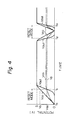
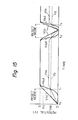
- the transistors Q 6 and Q 7 are cut off, so that the potential V a follows the power supply potential V CC .
- the potential V a is a definite value V a0 in accordance with the potential characteristics of MOS diodes. Since the saturation characteristics of the potential V a are better when the load transistor Q 1 has a larger resistance, it is preferable that the conductance g m of the transistor Q 1 be small.
- the inverter INV 1 receiving the potential V a , since its threshold potential V th is dependent on the power supply potential V CC , the potential V a intersects the threshold potential V th of the inverter INV 1 at the times t 1 , t 2 , and t 3 , so that the output V out of the inverter INV 1 is changed from high to low or vice versa. Thus, a reduction of the power supply potential V CC can be detected. Accordingly, when the output V out of the inverter INV 1 is shaped by the following inverters INV 2 , INV 3 , and INV 4 , a stepwise reset signal RST is obtained.
- the value of the power supply potential V CC at the time t 1 , t 2 , or t 3 is called a detection potential V D , which is, for example, 4 V.
- depletion-type transistors Q 21 Q 22 and Q 23 and enhancement-type transistors Q 24 , Q 25 , Q 26 , and Q 27 are added to the elements of Fig. 3, so as to compensate for manufacturing fluctuation.
- the transistors Q21 ' Q 24 , and Q 25 have the same charac- teristics as those of the transistors Q 1 ., Q 6 , and Q , respectively. Therefore, the potential V b is about the same as the potential V .
- the transistors Q 22 ' Q 23 , and Q 26 form an inverting-amplifier AM P . In this case, the transistor Q 23 is a feedback resistance.
- the gain of the inverting--amplifier AMP is set by the feedback resistance transistor Q 23 .
- the transistor Q 27 is interposed between the source of the transistor Q 8 and the ground, so that the threshold potential Vt h of the inverter INV 1 is also controlled by the conductance g m of the transistor Q 27 , which is controlled by the output V C of the inverting-amplifier AMP.
- the potential V C falls so as to reduce the conductance g m of the transistor Q 27 , i.e., to increase the threshold potential V th of the inverter INV 1 .
- the intersecting point is actually moved from P 1 to P 3 , so that the detection potential remains at V D .
- the gate of the transistor Q 26 can be also connected directly to the source of the transistor Q 1 .
- the transistors Q 21 , Q 24 , and Q 25 are omitted.
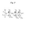
- resistors R 1 and R 2 are provided instead of the transistors Q 1 , Q 6 , and Q 7 of Fi g. 3.
- the inverter INV 4 of Fig. 3 is omitted. In this case, the output V out of the inverter INV 1 changes as shown in Fig. 8 in the opposite way as in Fig. 4.
- resistors R l ' and R 2 ' , and transistors Q 22 , Q 23 , Q 26 , and Q 27 are added to the elements of F ig. 7, so as to compensate for the manufacturing fluctuation of the circuit of Fig. 7. That is, the circuits of Figs. 7 and 9 correspond to the circuits of Figs. 3 and 5, respectively.
- enhancement-type transistors Q 31 and Q 32 and a depletion-type transistor Q 33 are provided instead of the resistors R 1 and R 2 of Fig. 7.
- the transistors Q 31 and Q 32 have gates connected to the drains thereof and, accordingly,are MOS diodes while the transistor Q 33 has a gate connected to the source thereof and, accordingly, serves as a load.
- the transistors Q 31 and Q 32 are cut off, so that the potential V a remains at the ground potential.
- the potential V a is a definite value V a0 in accordance with the MOS diode characteristics.
- the conductance g m of the transistor Q 33 be small.
- enhancement-type transistors Q 34 and Q 35 and a depletion-type transistor Q36 are provided instead of the resistors R 1 ' and R 2 1 of Fig. 9, so as to compensate for the manufacturing fluctuation of the circuit of Fig. 10.
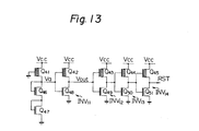
- the power-supply-potential detecting circuit 9 comprises P-channel transistors Q 41 through Q 45 and N-channel transistors Q 46 through Q 51 .
- the gate of the transistor Q41 is grounded and, accordingly, this transistor Q 41 serves as a resistance.
- the transistors Q 46 and Q 47 have gates connected to the drains thereof and, accordingly, serve as MOS diodes.
- the serial configuration of the two transistors Q 46 and Q 47 is also helpful in effectively driving the following stage C MOS inverter INV 11 formed by the transistors Q 42 and Q 48 .
- transistors Q 43 and Q 49 , Q 44 and Q 50 , and Q 45 and Q 51 also form CMOS inverters INV 12 , INV13 , and INV 14 , respectively, which inverters are, however, used for shaping the output V out of the inverter INV 11 so as to generate a reset signal RST.
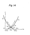
- the threshold potential V th of a standard CMOS inverter is half of the power supply potential V CC , i.e., V CC /2, which will be explained with reference to Fig. 14.
- the ordinate represents a current I
- the abscissa represents a potential such as the potential V a of Fig. 13.
- V thn is the threshold potential of the N-channel transistor Q 48
- V th p is the threshold potential of the P-channel transistor Q 42 .
- V a equals the threshold potential V th when the current I p flowing through the P-channel transistor Q 42 is the same as the current In flowing through the N-channel transistor Q 48 . That is, if
- the transistor Q 48 has about the same conductance. Contrary to this, even when the potential V a is definite,the transistor Q 42 is more deeply biased as the power supply potential V CC rises. As a result, the conductance of the transistor Q 42 becomes large, and, accordingly, the output V out is pulled up at the time t 1 . Even in this case, since the transistor Q 48 remains conductive, the change of the output V out of the inverter INV 11 is out slow. Therefore, the following inverters INV 12 , INV13 , and INV 14 shape this output V out so as to generate a stepwise reset signal RST.
- the threshold potential V th of the CMOS inverter such as INV 11 can be changed by changing the size of the P-channel transistor Q 42 or the N-channel transistor Q 48 .
- the size of the N -channel transistor Q 48 is increased, the current I n flowing therethrough is increased as indicated by a dotted line in Fig. 14.
- the intersecting point is moved from P 11 to P 12 , so as to reduce the threshold potential V th . Therefore, the detection potential V D is also reduced.
- the size of the P-channel transistor Q 42 is increased, the current I p flowing therethrough is increased as indicated by a dash-dotted line in Fig. 14.
- the threshold potential V th can be arbitrarily set within V thn to (V CC - Vt h p) in Fig. 14, so as to obtain a desired value of V D .
- P-channel transistors Q 52 through Q 54 and N-channel transistors Q 56 through Q60 are added to the elements of Fig. 13, so as to compensate for the manufacturing fluctuation of the circuit of Fig. 13, especially the manufacturing fluctuation of the transistors Q 46 and Q 47 .
- the threshold potential of each of the transistors Q 46 and Q 47 is changed by 10%, the potential V is changed as indicated by Va' in Fig. 17.
- the threshold potential V th of the inverter INV 11 remains unchanged, the intersecting point is moved from P 21 to P 22 , so that the detection potential is also moved from V D to V D '.
- the added transistors Q 52 through Q60 increase the threshold potential V th , so that the intersecting point is actually moved from P 21 to P23. Therefore, the detection potential V D remains at V D .
- the transistors Q 52 , Q 56 , and Q 57 have the same characteristics as those of the transistors Q 41 , Q46 and Q 47 , respectively. Therefore, the potential V b is the same as the potential V a .
- the transistors Q53 , Q 58 ' Q 59 ' and Q 55 form an inverting-amplifier AMP .
- the transistors Q 59 and Q 55 in combination form a feedback resistance and, accordingly, the gain of the inverting-amplifier AMP is set by this feedback resistance.
- the transistor Q 54 is interposed between the power supply V CC and the drain of the transistor Q42
- the transistor Q 60 is interposed between the source of the transistor Q 48 and the ground. The gates of these transistors Q 54 and Q 60 are commonly controlled by the output V C of the inverting--amplifier AMP.
- the conductance g m of the transistor Q 54 is reduced, while the conductance of the transistor Q 60 is increased.
- the resistance on the P-channel transistors Q 54 and Q 42 is reduced, while the resistance on the N-channel transistors Q 48 and Q 60 is increased. That is, the slope of the current I p becomes large, while the slope of the current I n becomes small, so that the intersecting point (Fig. 14) of the current I p and the I n is moved to the right side.
- the threshold potential of the inverter INV 11 is moved from V th to V th ', so that the intersecting point of the threshold potential of the inverter INV 11 and the output V a is moved from P 21 to P 23 ⁇ Thus, the detection potential is stabilized at V D .
- the increase ⁇ th from V th to V th ' is adjusted by the gain of the inverting-amplifier AMP or the parameters of the transistors Q 54 and Q 60 .
- the fluctuation of the threshold potential V th of the inverter INV 11 due to the transistors thereof invites the change of the slope of V th , which change is, however, not so large as that due to the manufacturing fluctuation of the transistors Q 41 , Q 46 , and Q 47 .
- the feedback resistance formed by the transistors Q 59 and Q 55 and the like are adjusted.
- the input of the inverting-amplifier AMP can be also connected directly to the source of the transistor Q 41 so as to omit the transistors Q 52 , Q 56 , and Q 57 ⁇
- the present invention has an advantage in that it is completely possible to check whether or not the one-chip semiconductor device incorporating a power-supplv-potential detecting circuit operates normally.
Landscapes
- Engineering & Computer Science (AREA)
- Theoretical Computer Science (AREA)
- Physics & Mathematics (AREA)
- General Engineering & Computer Science (AREA)
- General Physics & Mathematics (AREA)
- Semiconductor Integrated Circuits (AREA)
- Electronic Switches (AREA)
Applications Claiming Priority (4)
| Application Number | Priority Date | Filing Date | Title |
|---|---|---|---|
| JP57098649A JPS58221421A (ja) | 1982-06-09 | 1982-06-09 | 電源電圧検出回路 |
| JP98649/82 | 1982-06-09 | ||
| JP113308/82 | 1982-06-30 | ||
| JP57113308A JPS593646A (ja) | 1982-06-30 | 1982-06-30 | 集積回路の電源電圧検知リセツト方式 |
Publications (2)
| Publication Number | Publication Date |
|---|---|
| EP0096531A1 true EP0096531A1 (de) | 1983-12-21 |
| EP0096531B1 EP0096531B1 (de) | 1987-09-16 |
Family
ID=26439780
Family Applications (1)
| Application Number | Title | Priority Date | Filing Date |
|---|---|---|---|
| EP83303140A Expired EP0096531B1 (de) | 1982-06-09 | 1983-06-01 | Ein-Chip-Halbleitervorrichtung, die eine Versorgungsspannungsdetektorschaltung mit Rücksetzfunktion enthält |
Country Status (4)
| Country | Link |
|---|---|
| US (1) | US4551841A (de) |
| EP (1) | EP0096531B1 (de) |
| DE (1) | DE3373759D1 (de) |
| IE (1) | IE54444B1 (de) |
Cited By (9)
| Publication number | Priority date | Publication date | Assignee | Title |
|---|---|---|---|---|
| GB2163413A (en) * | 1984-05-04 | 1986-02-26 | Johnsen & Jorgensen | Closure assembly |
| EP0158512A3 (de) * | 1984-04-05 | 1987-11-19 | Mitsubishi Denki Kabushiki Kaisha | Rücksetzschaltung |
| EP0273574A1 (de) * | 1986-11-27 | 1988-07-06 | Seiko Instruments Inc. | System zum Einstellen des Anfangswertes für eine elektronische Einrichtung |
| EP0317437A3 (en) * | 1987-11-18 | 1990-07-11 | Fujitsu Limited | Reset signal generating circuit |
| EP0370737A3 (de) * | 1988-11-21 | 1990-10-31 | Nippon Motorola Ltd. | Niederspannungs-Sperrsteuerungsvorrichtung |
| EP0351157A3 (de) * | 1988-07-12 | 1991-12-04 | Sony Corporation | Integrierte Halbleiterschaltungen |
| EP0544380A3 (en) * | 1991-11-26 | 1993-11-24 | Sgs Thomson Microelectronics | An initialization circuit for memory registers |
| EP0591561A1 (de) * | 1992-09-30 | 1994-04-13 | Siemens Aktiengesellschaft | Integrierte Schaltung zur Erzeugung eines Reset-Signals |
| EP0700160A3 (de) * | 1994-08-05 | 1997-09-17 | Advanced Micro Devices Inc | Einschalt-Rücksetzschaltung |
Families Citing this family (42)
| Publication number | Priority date | Publication date | Assignee | Title |
|---|---|---|---|---|
| GB2145254A (en) * | 1983-08-17 | 1985-03-20 | Philips Electronic Associated | Domestic electrical appliance |
| US4766567A (en) * | 1984-04-19 | 1988-08-23 | Ltd. Nippondenso Co. | One-chip data processing device including low voltage detector |
| US4618953A (en) * | 1984-05-01 | 1986-10-21 | Pitney Bowes Inc. | Watchdog circuit |
| FR2571872B1 (fr) * | 1984-10-15 | 1987-02-20 | Sagem | Dispositif d'alimentation electrique de microprocesseurs |
| US4627060A (en) * | 1984-11-29 | 1986-12-02 | Baxter Travenol Laboratories, Inc. | Watchdog timer |
| US4926355A (en) * | 1987-07-02 | 1990-05-15 | General Datacomm, Inc. | Digital signal processor architecture with an ALU and a serial processing section operating in parallel |
| JP2579327B2 (ja) * | 1987-12-04 | 1997-02-05 | 富士通株式会社 | 半導体集積回路 |
| JPH01159716A (ja) * | 1987-12-16 | 1989-06-22 | Alpine Electron Inc | マイコンのリセット回路 |
| US4931975A (en) * | 1987-12-21 | 1990-06-05 | Johnson Service Company | Microprocessor-based controller with synchronous reset |
| US5051936A (en) * | 1987-12-21 | 1991-09-24 | Johnson Service Company | Microprocessor-based controller with synchronous reset |
| JPH01184415A (ja) * | 1988-01-18 | 1989-07-24 | Yamaha Corp | 電源モニタ回路および該回路を内蔵したロータリエンコーダ |
| JP2761924B2 (ja) * | 1989-06-08 | 1998-06-04 | キヤノン株式会社 | ユニット間通信装置 |
| JP2877378B2 (ja) * | 1989-09-29 | 1999-03-31 | 株式会社東芝 | パーソナルコンピュータ |
| JPH04109547A (ja) * | 1990-08-30 | 1992-04-10 | Sharp Corp | メモリデータ保護装置 |
| JPH04178114A (ja) * | 1990-11-09 | 1992-06-25 | Canon Inc | 電子機器 |
| JP2979709B2 (ja) * | 1991-05-17 | 1999-11-15 | 富士通株式会社 | Lsiの入出力回路 |
| JP2788680B2 (ja) * | 1991-06-10 | 1998-08-20 | キヤノン株式会社 | 電子機器及びそのデータ入出力制御方法 |
| DE69231230T2 (de) * | 1991-11-12 | 2001-03-01 | Microchip Technology Inc., Chandler | Einschaltverzoegerung fuer mikrokontroller |
| US5237698A (en) * | 1991-12-03 | 1993-08-17 | Rohm Co., Ltd. | Microcomputer |
| US5410713A (en) * | 1992-01-02 | 1995-04-25 | Smith Corona/Acer | Power-management system for a computer |
| US5408573A (en) * | 1992-06-17 | 1995-04-18 | Johnson Service Company | Integrated motor controller |
| US5309037A (en) * | 1992-07-08 | 1994-05-03 | International Business Machines Corporation | Power-on reset circuit with arbitrary output prevention |
| KR970003810B1 (ko) * | 1993-04-14 | 1997-03-22 | 삼성전자 주식회사 | 어드레스 천이 검출회로를 내장하는 불휘발성 반도체 집적회로 |
| DE4314533C1 (de) * | 1993-05-03 | 1994-05-19 | Siemens Ag | Schaltungsanordnung zur Überwachung der Versorgungsspannung einer Prozessoreinheit |
| JPH07160666A (ja) * | 1993-12-10 | 1995-06-23 | Zexel Corp | マイクロコンピュータのリセット装置 |
| US5717907A (en) * | 1994-08-17 | 1998-02-10 | Alcatel Network Systems, Inc. | Method and apparatus for generating a reset pulse responsive to a threshold voltage and to a system clock |
| US5552745A (en) * | 1994-09-21 | 1996-09-03 | International Business Machines Corporation | Self-resetting CMOS multiplexer with static output driver |
| US5606511A (en) * | 1995-01-05 | 1997-02-25 | Microchip Technology Incorporated | Microcontroller with brownout detection |
| US5838929A (en) * | 1995-06-01 | 1998-11-17 | Ast Research, Inc. | Upgrade CPU module with integral power supply |
| US5721502A (en) * | 1995-06-06 | 1998-02-24 | Analog Devices, Inc. | Voltage-controlled reset for logic state initialization |
| EP0882258B1 (de) * | 1995-12-29 | 2000-07-26 | Advanced Micro Devices, Inc. | Rücksetzschaltung für eine batterie-getriebene integrierte schaltung und verfahren zum rücksetzen dieser integrierten schaltung |
| DE19611942C2 (de) * | 1996-03-26 | 2003-02-20 | Daimler Chrysler Ag | Halbleiterschaltkreis für ein elektronisches Steuergerät |
| DE19627362C2 (de) * | 1996-07-06 | 1998-11-26 | Bosch Gmbh Robert | Schaltung zur Initialisierung und Überwachung eines Mikroprozessors |
| JPH10269767A (ja) * | 1997-03-19 | 1998-10-09 | Mitsubishi Electric Corp | 半導体装置 |
| JP2000165220A (ja) * | 1998-11-27 | 2000-06-16 | Fujitsu Ltd | 起動回路及び半導体集積回路装置 |
| US6335646B1 (en) * | 1999-04-28 | 2002-01-01 | Oki Electric Industry Co., Ltd. | Power-on reset circuit for generating a reset pulse signal upon detection of a power supply voltage |
| US7257740B2 (en) * | 2002-06-10 | 2007-08-14 | Nxp B.V. | Circuit for detecting ground offset of parts of a network |
| JP2005039635A (ja) * | 2003-07-16 | 2005-02-10 | Matsushita Electric Ind Co Ltd | パワーオンリセット回路 |
| US20060055438A1 (en) * | 2004-09-14 | 2006-03-16 | Yongcong Chen | Power-on reset circuit |
| US7526674B2 (en) * | 2005-12-22 | 2009-04-28 | International Business Machines Corporation | Methods and apparatuses for supplying power to processors in multiple processor systems |
| US8504807B2 (en) | 2009-12-26 | 2013-08-06 | Intel Corporation | Rotate instructions that complete execution without reading carry flag |
| KR101646910B1 (ko) * | 2011-01-11 | 2016-08-09 | 페어차일드코리아반도체 주식회사 | 파워 온 리셋 회로를 포함하는 반도체 소자 |
Citations (5)
| Publication number | Priority date | Publication date | Assignee | Title |
|---|---|---|---|---|
| US4013902A (en) * | 1975-08-06 | 1977-03-22 | Honeywell Inc. | Initial reset signal generator and low voltage detector |
| US4048524A (en) * | 1976-04-21 | 1977-09-13 | National Semiconductor Corporation | MOS voltage level detecting and indicating apparatus |
| US4173756A (en) * | 1976-12-11 | 1979-11-06 | Tokyo Shibaura Electric Co., Ltd. | Abnormal voltage detection circuit |
| US4296338A (en) * | 1979-05-01 | 1981-10-20 | Motorola, Inc. | Power on and low voltage reset circuit |
| US4301380A (en) * | 1979-05-01 | 1981-11-17 | Motorola, Inc. | Voltage detector |
Family Cites Families (6)
| Publication number | Priority date | Publication date | Assignee | Title |
|---|---|---|---|---|
| US4200916A (en) * | 1976-07-01 | 1980-04-29 | Gulf & Western Industries, Inc. | Programmable controller using microprocessor |
| US4244050A (en) * | 1978-02-27 | 1981-01-06 | The Bendix Corporation | Dual voltage regulator with low voltage shutdown |
| US4234920A (en) * | 1978-11-24 | 1980-11-18 | Engineered Systems, Inc. | Power failure detection and restart system |
| JPS56162122A (en) * | 1980-05-16 | 1981-12-12 | Canon Inc | Electronic apparatus equipped with printing device |
| US4429366A (en) * | 1981-04-09 | 1984-01-31 | Westinghouse Electric Corp. | Microprocessor-based load management terminal with reset |
| US4410991A (en) * | 1981-06-03 | 1983-10-18 | Gte Laboratories Incorporated | Supervisory control apparatus |
-
1983
- 1983-06-01 DE DE8383303140T patent/DE3373759D1/de not_active Expired
- 1983-06-01 EP EP83303140A patent/EP0096531B1/de not_active Expired
- 1983-06-09 IE IE1358/83A patent/IE54444B1/en not_active IP Right Cessation
- 1983-06-09 US US06/502,591 patent/US4551841A/en not_active Expired - Lifetime
Patent Citations (5)
| Publication number | Priority date | Publication date | Assignee | Title |
|---|---|---|---|---|
| US4013902A (en) * | 1975-08-06 | 1977-03-22 | Honeywell Inc. | Initial reset signal generator and low voltage detector |
| US4048524A (en) * | 1976-04-21 | 1977-09-13 | National Semiconductor Corporation | MOS voltage level detecting and indicating apparatus |
| US4173756A (en) * | 1976-12-11 | 1979-11-06 | Tokyo Shibaura Electric Co., Ltd. | Abnormal voltage detection circuit |
| US4296338A (en) * | 1979-05-01 | 1981-10-20 | Motorola, Inc. | Power on and low voltage reset circuit |
| US4301380A (en) * | 1979-05-01 | 1981-11-17 | Motorola, Inc. | Voltage detector |
Cited By (11)
| Publication number | Priority date | Publication date | Assignee | Title |
|---|---|---|---|---|
| EP0158512A3 (de) * | 1984-04-05 | 1987-11-19 | Mitsubishi Denki Kabushiki Kaisha | Rücksetzschaltung |
| GB2163413A (en) * | 1984-05-04 | 1986-02-26 | Johnsen & Jorgensen | Closure assembly |
| EP0273574A1 (de) * | 1986-11-27 | 1988-07-06 | Seiko Instruments Inc. | System zum Einstellen des Anfangswertes für eine elektronische Einrichtung |
| EP0317437A3 (en) * | 1987-11-18 | 1990-07-11 | Fujitsu Limited | Reset signal generating circuit |
| EP0351157A3 (de) * | 1988-07-12 | 1991-12-04 | Sony Corporation | Integrierte Halbleiterschaltungen |
| US5381551A (en) * | 1988-07-12 | 1995-01-10 | Sony Corporation | Semiconductor integrated circuit including an arbitrate circuit for giving priority to a plurality of request signals |
| EP0370737A3 (de) * | 1988-11-21 | 1990-10-31 | Nippon Motorola Ltd. | Niederspannungs-Sperrsteuerungsvorrichtung |
| EP0544380A3 (en) * | 1991-11-26 | 1993-11-24 | Sgs Thomson Microelectronics | An initialization circuit for memory registers |
| EP0591561A1 (de) * | 1992-09-30 | 1994-04-13 | Siemens Aktiengesellschaft | Integrierte Schaltung zur Erzeugung eines Reset-Signals |
| US5442312A (en) * | 1992-09-30 | 1995-08-15 | Siemens Ag | Integrated circuit for generating a reset signal |
| EP0700160A3 (de) * | 1994-08-05 | 1997-09-17 | Advanced Micro Devices Inc | Einschalt-Rücksetzschaltung |
Also Published As
| Publication number | Publication date |
|---|---|
| DE3373759D1 (en) | 1987-10-22 |
| IE54444B1 (en) | 1989-10-11 |
| IE831358L (en) | 1983-12-09 |
| US4551841A (en) | 1985-11-05 |
| EP0096531B1 (de) | 1987-09-16 |
Similar Documents
| Publication | Publication Date | Title |
|---|---|---|
| EP0096531A1 (de) | Ein-Chip-Halbleitervorrichtung, die eine Versorgungsspannungsdetektorschaltung mit Rücksetzfunktion enthält | |
| US4574273A (en) | Circuit for changing the voltage level of binary signals | |
| US4972100A (en) | Data output buffer circuit for byte-wide memory | |
| US4675544A (en) | CMOS-inverter | |
| US6300796B1 (en) | High voltage PMOS level shifter | |
| EP0103236A2 (de) | Logische Schaltung | |
| JPH05136685A (ja) | レベル変換回路 | |
| JPH0342015B2 (de) | ||
| US4849653A (en) | Semiconductor circuit device for preventing an output of a bistable circuit from becoming unstable | |
| GB2123634A (en) | Master-slave flip-flop | |
| US4578694A (en) | Inverter circuit provided with gate protection | |
| US5936456A (en) | Output driver circuit in semiconductor device | |
| US4786825A (en) | CMOS Schmitt trigger circuit using ratioed currents to establish switching thresholds | |
| US5734280A (en) | Semiconductor integrated circuit device having power on reset circuit | |
| US4767950A (en) | MOS inverter circuit having two different supply voltages | |
| JPS5928986B2 (ja) | 半導体集積回路 | |
| KR100298444B1 (ko) | 입력 버퍼 회로 | |
| US4996446A (en) | Semiconductor device having a reverse bias voltage generator | |
| US6335649B1 (en) | Schmitt trigger circuit | |
| US4859882A (en) | Sense amplifier | |
| KR100223501B1 (ko) | 반도체 집적 회로 | |
| US7737734B1 (en) | Adaptive output driver | |
| US5412264A (en) | Signal input/output circuit for semiconductor integrated circuit | |
| US5929685A (en) | Mode setting circuit | |
| KR940001196Y1 (ko) | 프로그래머블 문턱전압 조정 입력회로 |
Legal Events
| Date | Code | Title | Description |
|---|---|---|---|
| PUAI | Public reference made under article 153(3) epc to a published international application that has entered the european phase |
Free format text: ORIGINAL CODE: 0009012 |
|
| AK | Designated contracting states |
Designated state(s): DE FR GB |
|
| 17P | Request for examination filed |
Effective date: 19840521 |
|
| GRAA | (expected) grant |
Free format text: ORIGINAL CODE: 0009210 |
|
| AK | Designated contracting states |
Kind code of ref document: B1 Designated state(s): DE FR GB |
|
| REF | Corresponds to: |
Ref document number: 3373759 Country of ref document: DE Date of ref document: 19871022 |
|
| ET | Fr: translation filed | ||
| PLBE | No opposition filed within time limit |
Free format text: ORIGINAL CODE: 0009261 |
|
| STAA | Information on the status of an ep patent application or granted ep patent |
Free format text: STATUS: NO OPPOSITION FILED WITHIN TIME LIMIT |
|
| 26N | No opposition filed | ||
| PGFP | Annual fee paid to national office [announced via postgrant information from national office to epo] |
Ref country code: GB Payment date: 19930521 Year of fee payment: 11 |
|
| PGFP | Annual fee paid to national office [announced via postgrant information from national office to epo] |
Ref country code: FR Payment date: 19930629 Year of fee payment: 11 |
|
| PGFP | Annual fee paid to national office [announced via postgrant information from national office to epo] |
Ref country code: DE Payment date: 19930830 Year of fee payment: 11 |
|
| PG25 | Lapsed in a contracting state [announced via postgrant information from national office to epo] |
Ref country code: GB Effective date: 19940601 |
|
| GBPC | Gb: european patent ceased through non-payment of renewal fee |
Effective date: 19940601 |
|
| PG25 | Lapsed in a contracting state [announced via postgrant information from national office to epo] |
Ref country code: FR Effective date: 19950228 |
|
| PG25 | Lapsed in a contracting state [announced via postgrant information from national office to epo] |
Ref country code: DE Effective date: 19950301 |
|
| REG | Reference to a national code |
Ref country code: FR Ref legal event code: ST |