EP0096760A2 - Binäre logische Struktur mit programmierbaren logischen Anordnungen zur Mikrobefehlerzeugung - Google Patents
Binäre logische Struktur mit programmierbaren logischen Anordnungen zur Mikrobefehlerzeugung Download PDFInfo
- Publication number
- EP0096760A2 EP0096760A2 EP83104958A EP83104958A EP0096760A2 EP 0096760 A2 EP0096760 A2 EP 0096760A2 EP 83104958 A EP83104958 A EP 83104958A EP 83104958 A EP83104958 A EP 83104958A EP 0096760 A2 EP0096760 A2 EP 0096760A2
- Authority
- EP
- European Patent Office
- Prior art keywords
- programmable logic
- binary
- array
- encode
- decode
- Prior art date
- Legal status (The legal status is an assumption and is not a legal conclusion. Google has not performed a legal analysis and makes no representation as to the accuracy of the status listed.)
- Withdrawn
Links
- 238000003491 array Methods 0.000 title claims abstract description 17
- 230000006870 function Effects 0.000 claims abstract description 13
- 230000004048 modification Effects 0.000 claims description 4
- 238000012986 modification Methods 0.000 claims description 4
- 240000007320 Pinus strobus Species 0.000 description 11
- 238000010276 construction Methods 0.000 description 8
- 230000008901 benefit Effects 0.000 description 7
- 238000010586 diagram Methods 0.000 description 7
- 239000000872 buffer Substances 0.000 description 5
- 230000009467 reduction Effects 0.000 description 5
- 238000000638 solvent extraction Methods 0.000 description 4
- 230000000295 complement effect Effects 0.000 description 3
- 230000007246 mechanism Effects 0.000 description 3
- 230000004044 response Effects 0.000 description 3
- 239000004065 semiconductor Substances 0.000 description 3
- 230000008878 coupling Effects 0.000 description 2
- 238000010168 coupling process Methods 0.000 description 2
- 238000005859 coupling reaction Methods 0.000 description 2
- 235000019988 mead Nutrition 0.000 description 2
- 230000003068 static effect Effects 0.000 description 2
- 210000003462 vein Anatomy 0.000 description 2
- 241000947840 Alteromonadales Species 0.000 description 1
- 208000034530 PLAA-associated neurodevelopmental disease Diseases 0.000 description 1
- 230000009471 action Effects 0.000 description 1
- 230000004913 activation Effects 0.000 description 1
- 230000008859 change Effects 0.000 description 1
- 230000000694 effects Effects 0.000 description 1
- 230000010354 integration Effects 0.000 description 1
- 230000001788 irregular Effects 0.000 description 1
- 230000002093 peripheral effect Effects 0.000 description 1
- 238000000926 separation method Methods 0.000 description 1
- 230000001550 time effect Effects 0.000 description 1
Images


Classifications
-
- H—ELECTRICITY
- H03—ELECTRONIC CIRCUITRY
- H03K—PULSE TECHNIQUE
- H03K19/00—Logic circuits, i.e. having at least two inputs acting on one output; Inverting circuits
- H03K19/02—Logic circuits, i.e. having at least two inputs acting on one output; Inverting circuits using specified components
- H03K19/173—Logic circuits, i.e. having at least two inputs acting on one output; Inverting circuits using specified components using elementary logic circuits as components
- H03K19/177—Logic circuits, i.e. having at least two inputs acting on one output; Inverting circuits using specified components using elementary logic circuits as components arranged in matrix form
- H03K19/17704—Logic circuits, i.e. having at least two inputs acting on one output; Inverting circuits using specified components using elementary logic circuits as components arranged in matrix form the logic functions being realised by the interconnection of rows and columns
- H03K19/17708—Logic circuits, i.e. having at least two inputs acting on one output; Inverting circuits using specified components using elementary logic circuits as components arranged in matrix form the logic functions being realised by the interconnection of rows and columns using an AND matrix followed by an OR matrix, i.e. programmable logic arrays
Definitions
- This invention relates to binary logic structures formed on large scale integration (LSI) semiconductor integrated chips of the type used in digital computers, digital data processing systems, digital control systems and the like. It relates particularly to binary logic structures employing programmable logic arrays useful in the microword generation portion of microprogrammed data processors and other microprogrammed digital systems.
- LSI large scale integration
- Programmable logic arrays are useful mechanisms for implementing complex binary logic functions on semiconductor integrated circuit chips. They provide a regular and orderly structure for implementing irregular and complex combinational logic functions. They are more flexible and are easier to design than are other types of logic structures.
- a typical programmable logic array (PLA) and some of its uses are described at pages 79-88 of a textbook entitled Introduction to VLSI Systems, by Mead and Conway, published by Addidon-Wesley Publishing Company, Reading, Massachusetts 1980.
- the present invention provides a new and improved binary logic structure which uses programmable logic arrays (PLA'S) in such a way that the structure as a whole requires less space on an integrated circuit chip.
- This logic structure is comprised of an encode programmable logic array responsive to a first group of binary input signals for producing a smaller number of binary signals which are encoded to identify different binary value combinations for the first group of binary input signal, and a decode programmable logic array responsive to a second group of binary input signals and to the encoded binary signals produced by the encode programmable logic array for producing binary output signals representing logical functions of binary input signals in both the first and second groups.
- the second PLA Because of the smaller number of bits in the encoded group, less chip space is required for the second PLA than would otherwise be the case. In particular, the reduction in chip space required for the second PLA is greater than the chip space occuppied by the first or encode PLA. Thus, the two PLA'S in cascade require less chip space than would an equivalent single PLA.
- a first group of binary input signals are supplied to a first set of inputs of the AND array 11 by way of a first multiline input bus E.
- a second group of binary input signals are supplied to a second set of inputs of the AND array 11 by way of a second multiline input bus F.
- Multiple binary output signals are produced by the OR array 12 and appear on the multiline output bus M.
- the AND array 11 includes two internal input signals lines for each signal line in the input buses E and F.
- One such internal input line carries the true value of the input signal and the other such internal input line carries the complement value of the input signal.
- the AND array 11 includes an input bit partitioner which receives the input signals on the buses E and F and provides the true and complement values of such signals to the internal input signal lines in the AND array 11.
- the other set of internal signal lines in the AND array 11 are the so-called "word" lines G. These cross the internal input lines at right angles thereto. These input lines and word lines are formed at differents levels on the integrated circuit chip so that they are not in electrical contact with one another.
- the logic functions provided by the AND array 11 are determined by the locations and connections of transistors which are formed on the integrated circuit chip for purposes of coupling each word line to one or more of the internal input signal lines. These transistors are located and connected so that the resultant signal on each word line represents a desired logical function of one or more of the input signals on the input buses E and F.
- the OR array 12 is also comprised of two sets of signal lines which cross each other at right angles to form a rectangular grid pattern.
- the input set of such signal lines are the word lines G and the output set of such signal lines are the OR array output lines M.
- the word lines G within the OR array 12 cross the output lines M at a different level on the chip so that there is no direct electrical contact therebetween.
- the OR'ing functions provided by the OR array 12 are determined by the locations and connections of transistors which are formed on the integrated circuit chip for coupling various ones of the word lines G to various ones of the output lines M.
- the signal on each of the word lines G can be thought of as being the AND function of some combination of the true and complement values of one or more of the input signals appearing on the input buses E and F.
- the output signals appearing on each of the OR array output lines M can be thought of as being the OR function of the signals appearing on one or more of the word lines G.
- the AND array 11 abuts the OR array 12 with no wasted space between the arrays. The separation shown in the drawing is for convenience of explanation only.
- the relative physical size that is, the relative amount of chip space occuppied by the AND array 11 is a function of the total number of input lines (buses E and F) and the total number of word lines (bus G).
- the relative chip space or area for the AND array 11 is proportional to 2(E+F)G, where E, F and G represent the numbers of lines in the buses E, F and G, respectively.
- the factor of "2" is included because, for single bit partitioning, the AND array 11 has two internal input signal lines for each line in each of the buses E and F.
- the relative chip space or area required for the input lines in the bus E is proportional to 2EG.
- the relative size of the OR array 12 is proportional to GM, where M denotes the number of lines in the output bus M.
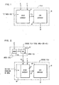
- FIG. 2 there is shown an embodiment of binary logic structure constructed in accordance with the present invention. It includes a first PLA 13 coupled in cascade with a second PLA 14. As will be seen, this will, under the proper conditions, result in the use of less space on the integrated circuit chip, as compared to the logic structure of Fig. 1. Both of the PLA's 13 and 14 are formed on one and the same integrated circuit chip. For sake of a name, the first PLA 13 will be referred to herein as an "encode" PLA and the second PLA 14 will be referred to as a "decode" PLA. Each of these PLA's 13 and 14 has the same general form of internal construction as was described above for the PLA 10 of Fi g . 1.
- the encode PLA 13 includes an input AND array 15, an output OR array 16 and a plurality of word lines located in a multiline bus J for connecting the outputs of the AND array 15 to the corresponding inputs of the OR array 16.
- the decode PLA 14 includes an input AND array 17, an output OR array 18 and a plurality of word lines located in a multiline bus G for connecting the outputs of the AND array 17 to the corresponding inputs of the OR array 18.
- Single-bit partitioning is assumed for each of the AND arrays 15 and 17.
- Each of the AND arrays 15 and 17 is of the same general form of internal construction as was described for the case of the AND array 11 of Fig. 1.
- each of the OR arrays 16 and 18 has the same general form of internal construction as was described above for the OR array 12 of Fig. 1.
- the numbers of signal lines in the buses E, F, G and M of Fig. 2 are assumed to be the same as the numbers of signal lines in the buses E, F, G and M, respectively, of Fig. 1.
- the encode PLA 13 is responsive to a first group of binary input signals E for producing a smaller number of binary signals K which are encoded to identify different binary value combinations for the first group of binary input signals E.
- the decode programmable logic array 14 is responsive to a second group of binary input signals F and to the encoded binary signals K produced by the encode PLA 13 for producing binary output signals M representing logical functions of binary input signals in both the first and second groups E and F.
- the use of the encode PLA 13 to more tightly encode the binary input signals E reduces the number of signal lines K running to the input of the AND array 17 in the second PLA 14, this reduction being represented by the factor (E-K), where E and K represent the numbers of signal lines in the buses E and K, respectively. This, in turn, reduces the amount of chip space required for the AND array 17. This reduction or decrease in area is proportional to 2(E-K)G. This reduction in area is represented by the broken line boundary 19. This reduction, however, does not represent the net saving of chip space.
- the use of the encode PLA 13 requires some chip space.
- the relative chip space occuppied by the encode PLA 13 is proportional to (2E+K)J. In order to obtain a net saving in chip space, this space required for the encode PLA 13 must be less than the decrease in space realized for the decode AND array 17. In a goodly number of applications, this condition can be satisfied.
- the denominator term 2EG represents the Fig. 1 case where only a single PLA is employed and all of the binary input signals E are supplied to its AND array 11. This 2EG factor represents the area required in the AND array 11 for the input signals E.
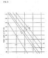
- Fig. 3 is a graph showing the percent saving of chip space for different values of the ratio K/E. Various lines are plotted for different values of the ratio G/J. These lines were plotted using the above-given percent saving equation.
- the encode PLA 13 should be relatively small compared to the decode PLA 14.
- the primary aspect in meeting this criteria is that the number of word lines J in the encode PLA 13 must be substantially smaller than the number of word lines G in the decode PLA 14.
- the relative numbers of word lines in the two PLA's is determined by the natures of the two groups of binary input signals E and F.
- the signals in group F should be tightly encoded and each code value should be used with a high degree of frequency in determining the resultant output signals produced by the decode OR array 18.
- tightly encoded is meant that practically every binary value combination for the signals in group F are used. For example, if group F has five signals (5 bits), this can provide 32 different binary code values or combinations. To be tightly encoded, substantially all 32 such binary code values should be used.
- the signal in group E should be loosely encoded and should be used less often in determining the resultant output from the decode OR array 18.
- loosely encoded is meant that many of the different possible binary code values for the group E signals are not used. Assume, for example, that there are 16 signals (16 bits) in group E and that only some 200 out of the total possible 65,536 different binary code value are used. In this case, the input signals in group E are said to be loosely encoded. In such a case, the encode PLA 13 acts to tighten up the encoding by producing a different unique encoded identification signal only for those 200 code combinations which are actually used. In this manner, the number of input signal lines for group E can be reduced from 16 to 8. In other words, the input bus K for the decode PLA will have only 8 signal lines, as opposed to the original 16 signal lines in the input bus E.
- the present invention can be used in the control unit of a digital data processor to provide an improved microword generation mechanism.
- the digital system of Fig. 4 is a microprogrammed data processor 20 wherein a sequence of microwords are used to control the execution of each system or processor instruction.
- This data processor 20 includes a data flow unit 21, a main storage unit 22, an input/output (I/O) unit 23 and a control unit 24.
- the data flow unit 21 is sometimes called a central processing unit (CPU) and includes such things as an arithmetic and logic unit (ALU), various hardware registers and counters, a local storage unit, and a bus system interconnecting these items with one another.
- the data flow unit 21 is the unit that does the adding, substracting, rearranging and other manipulation of the data to produce the desired results.
- Control unit 24 controls the operation of the data flow unit 21, the main storage unit 22 and the I/O unit 23 by means of various control point signals which are supplied by way of respective multiline control buses 25, 26 and 27 to the various functional elements located in these units 21, 22 and 23.
- Control unit 24 includes microword generation apparatus for producing a sequence of microwords for each system instruction, in this case, processor instruction, to be executed. These microwords, in turn, produce the control point signals which control the elemental operations in the other data processor units.
- the user program to be performed by the data processor 20 is initially loaded into the main storage unit 22 from one of the peripheral units (not shown) coupled to the I/O unit 23 by way of an I/O bus 28. This initial loading is accomplished by way of the data flow unit 21. After such initial loading, the user program is performed by reading from the main storage unit 22 in a sequential manner the various processor instructions which make up the user program. Each processor instruction, in its turn, is read out of the main storage unit 22 and loaded into an instruction register 29 located in the data flow unit 21. The processor instruction resident in the instruction register 29, or at least the effective operation code portion thereof, is supplied to the control unit 24 by way of a multiline bus 30 to identify to the control unit 24 the particular processor instruction to be executed.
- Loading of a new processor instruction into the instruction register 29 is accomplished by way of a control point signal which is supplied by way of a control line 31 to a load control terminal of the instruction register 29.
- the data flow unit 21, the I/O unit 23 and the control unit 24 can all be fabricated on one and the same integrated circuit chip. In order to accomplish this, the circuit structures formed on the chip must be designed to minimize their usage of chip space.
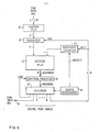
- FIG. 5 there is shown in greater detail a representative form of construction for the control unit 24 of Fig. 4.
- This construction includes a first embodiment of microword generation apparatus constructed in accordance with the present invention.
- This improved microword generation apparatus includes an encode PLA 32, a decode PLA 33 and sequence counter circuitry 34.
- each of the PLA's 32 and 33 is assumed to be a "static" PLA, as opposed to a “dynamic” or clocked PLA. In making this assumption, it is to be understood that the present invention is also applicable to the case of dynamic PLA's.
- the encode PLA 32 is responsive to a plural-bit system instruction to be executed for producing a plural-bit instruction identification signal uniquely representative of such system instruction but having a smaller number of bits than the system instruction.
- the system instruction is the processor instruction which is being supplied to the input of the encode PLA 32 from the instruction register 29 by way of the multibit or multiline bus 30.
- the instruction identification signal produced by the encode PLA 32 is supplied by way of a multi-stage binary register 35 to a first set of inputs of the AND array in the decode PLA 33.
- the processor instruction supplied to the encode PLA 32 may be, for example, a 16-bit binary word.
- the particular data processor being considered may have, for example, 200 different processor instructions in its instruction repertoire.
- the input bus E would be a 16-line bus
- the output bus K would be an 8-line bus
- the register 35 would be an 8-bit binary register for receiving the 8-bit instruction identification signal produced by the encode PLA 32.
- the sequence counter 34 is a plural-bit binary counter for supplying plural-bit binary number signals to a second set of inputs of the AND array in the decode PLA 33.
- the sequence counter 34 may be, for example, a 6-bit counter for supplying in a parallel manner a 6-bit number by way of the input bus F to the decode PLA 33.
- the bus F is a 6-line bus.
- the decode PLA 33 is responsive to the instruction identification signal from the encode PLA 32 and to the number signals from the sequence counter 34 for producing a sequence of microwords for each processor instruction to be executed.
- the microwords appear one at a time at the output of the OR array in the decode PLA 33.
- Each microword may have a width of, for example, 60 bits.
- the output bus M is a 60-line bus.
- the control unit embodiment of Fig. 5 further includes control circuitry responsive one at a time to the microwords from the decode PLA 33 for producing for each micrword a plurality of control point signals for controlling for one microword cycle the operation of the digital data processing system of Fig. 4.
- This control circuitry includes a multibit control register 36, a decoder 37 and a clock pulse generator 38.
- the number of bit positions or stages in the control register 36 is the same as the number of bit positions in a single microword.
- the microword appearing at the output of the decode PLA 33 is loaded into the control register 36 at the end of the preceding microword cycle.
- the microword residing in control register 36 drives the decoder 37 to cause the decoder 37 to produce the particular control point signals for that particular microword.
- each microword will include several encoded plural-bit control fields. Decoder 37 decodes the encoded fields to produce the appropriate individual control point signals. Any non-encoded or bit-significant bits in the microword will he supplied straight through by the decoder 37.
- the clock generator 38 supplies the clock pulses which determine the points in time at which the control point signals actually appear at the output of the decoder 37. In some data processors, there is one clock pulse per microword cycle, while in other data processors there are a. group of time spaced clock pulses for each microword cycle. Decoder 37 will typically have a relatively large number of control point output lines. In a typical data processor, there may be a hundred or more such output lines. For any given microword, only a relatively small number of these control point lines will be activated to produce the desired control actions for that particular microword.
- the clock generator 38 also supplies clock pulses to the increment input terminal of the sequence counter 34 for increasing the count in the sequence counter 34 by a value of one count for each microword cycle.
- the timing is such that immediately after a particular microword is loaded into the control register 36, the sequence counter 34 is incremented by one to enable the decode PLA 33 to commence producing the next microword.
- the repeated incrementing of the sequence counter 34 causes the decode PLA 33 to produce a sequence of microwords for any given instruction identification signal residing in the register 35.
- the last microword in the sequence will, among other things, cause the control point line 39 to be activated to load the next instruction identification signal into the register 35 and to reset the sequence counter 34 to a zero count condition.
- a new instruction identification signal is produced by the encode PLA 32 and, at the appropriate point in time, is loaded into the register 35.
- the loading of the new processor instruction into the instruction register 29 is done at some appropriate point during the occurrence of the microword sequence for the processor instruction currently being executed. In other words, some of the microwords being produced for the currently executing processor instruction also cause activation of the appropriate control point signal lines for fetching the next processor instruction from the main storage unit 22 and loading it into the instruction register 29.
- the encode PLA 32 then operates to produce the appropriate instruction identification signal for this next processor instruction.
- the last microword for the currently executing instruction is effective to load this next instruction identification signal into the encode PLA output register 35 and to reset the sequence counter 34 to commence the generation of the microword sequence for this next processor instruction.
- the encode PLA 32 has 200 word lines and its encoded output K has a width of 8 bits.
- the decode PLA 33 may have, for example, on the order of 1000 word lines. This makes G (number of decode PLA word lines) equal to 5 times J (the number of encode PLA word lines). Since the ratio K/E is equal to 0.5, this gives a percent saving of chip space of approximately 25% as seen from the graph of Fig. 3.
- the use of the encode PLA 32 in cascade with the decode PLA 33 provides a 25% savings of chip space as compared to the case where the encode PLA 32 is omitted and the processor instruction is supplied without modification to the decode PLA 33.
- the decode PLA 33 would need to have a much wider input AND array to accommodate the increased number of input bits.
- a rule of thumb for PLA's is that the larger the PLA becomes in size, the slower is its response time (the time required to produce a valid output following a change in the input).
- a decode PLA 33 having 1000 word lines would begin to show the effect of this rule. In particular, it would have a slower response time than may be desirable for some applications.
- the next embodiment to be described herein shows a way of reducing this slower response time effect. In particular, this is accomplished by replacing the larger decode PLA 33 by a plurality of smaller decode PLA,s which are operated in an overlapped time-multiplexed manner.
- All of the hardware units and elements shown in Fig. 5 are preferably formed on a single integrated circuit chip.
- FIG. 6 there is shown a functional block diagram of a second embodiment of microword generation apparatus which is constructed in accordance with the present invention and which may be used to provide the control unit 24 of Fig. 4.
- the Fig. 6 embodiment employs a decode PLA mechanism which is comprised of four smaller decode PLA's 40,41,42 and 43 which are operated in an overlapped parallel manner.
- the decode PLA's 40-43 are labeled as the A, B, C and D decode PLA's, respectively. These different decode PLA's 40-43 produce different ones of the microwords needed to execute a given processor instruction. In particular, the microwords from the different decode PLA's 40-43 are used in a repeating A-B-C-D sequence.
- the decode PLA's 40-43 are driven in a parallel manner by an encode PLA 44 and a register 45. These correspond respectively to the encode PLA 32 and the register 35 of Fig. 5.
- the encode PLA 44 produces a plural-bit instruction identification signal on bus K having a smaller number of bits than the processor instruction on bus E.
- the second inputs of the decode PLA's 40-43 are driven by the plural-bit number signals which are produced by a sequence counter 46 which corresponds to the sequence counter 34 of Fig. 5.
- the sequence count numbers for the last two decode PLA's 42 and 43 are supplied by way of a register 47. This is done to adjust the timing to take into account the overlapped operation of the different decode PLA's.
- the Fig. 6 embodiment includes two additional PLA's, namely, a first cycle PLA 48 and a second cycle PLA 49.
- the first cycle PLA 48 produces the first and only the first microword needed in the execution of a given processor instruction.
- the second cycle PLA 49 produces the second and only the second microword needed for such processor instruction.
- the decode PLA t s 40-43 provide the remainder of the microwords needed to execute the instruction.
- the microword sequence for any given processor instruction is 1-2-A-B-C-D-A-B-C-D..., where 1 and 2 denote the microwords produced by the first and second cycle PLA's 48 and 49, respectively.
- first and second cycle PLA's 48 and 49 are relatively small fast-acting PLA's which are driven directly by the processor instruction in the instruction register 29. This enables the first two microwords to be produced very quickly. This allows more time for the other PLA's to commence producing the remainder of the microwords for a given processor instruction.
- the decode PLA's 40-43 and the first and the second cycle PLA's 48 and 49 are dynamic or clocked PLA's.
- each uses a set of four time-spaced non-overlapping clocking pulses (PCI-PC4) to produce each valid output bit pattern.
- the clock pulse sets for the successive ones of the PLA's 48,49,40,41,42 and 43 are offset relative to one another by one microword cycle so that the PC1 pulse for the second PLA 49 coincides with the PC2 pulse for the first PLA 48, the PC1 pulse for the third PLA 40 coincides with the PC2 pulse for the second PLA 49, etc.
- the internal operations for the PLA's 48,49,40,41,42 and 43 are offset but overlapped in time.
- These PC1-PC4 PLA internal clocking pulses are obtained from PLA clock logic 50 driven by clock generator 57.
- the encode PLA 44 may also be a dynamic PLA but for simplicity of explanation herein, is assumed to be a static PLA.
- control registers 51 and 52 are employed in the Fig. 6 embodiment.
- a "A” set is represented by control registers 51 and 52 and a decoder 53.
- a "B” set is represented by control register 54 and 55 and a decoder 56.
- the control unit of Fig. 6 is driven by a two-phase nonoverlapping clock generator 57. It produces two sets of interleaved but nonoverlapping clock pulses, one set being Set A and the other being Set B.
- the A clock pulses periodically enable a set of A gates 58 and the B clock pulses periodically enable a set of B gates 59, such enablings being in an interleaved but non-overlapping manner.
- the A decoder 53 and the B decoder 56 are caused to provide the control point signals in an alternating A-B-A-B manners. Many of the control point lines from the A decoder 53 are OR'ed with their counterparts from the B decoder 56 so that many of the units in the Fig. 4 data processor can receive their control point signals during either the A or the B clock phase.
- the first cycle PLA 48 and the A and C decode PLA's 40 and 42 supply their microwords one at a time to the A control register 51. Each microword, in turn, is passed to the second A control register 52 to drive the A decoder 53 to produce the output control point signals which are passed by the A gates 58 during the A clock phases.
- the second cycle PLA 49, the B decode PLA 41 and the D decode P LA 43 supply their microwords one at a time to the first B control register 54, from whence they are transferred to the second B control register 55 to drive the B decoder 56 to produce the control point signals which are passed by the B gates 59 during the B clock phases.
- each microword produces a control point signal which is referred to herein as a PLA output strobe signal.
- This strobe signal selects the PLA which is to supply the next microword to its associated control register.
- the PLA strobes from the A decoder 53 select between the PLA's 48, 40 and 42 to obtain the next microword for the A control register 51.
- the first cycle PLA 48 is selected to provide only the first microword needed for any given processor instruction.
- the microwords for the A control register 51 are alternately taken from the A and C decode P L A's 40 and 42.
- the P LA output strobes from the A decoder 53 are identified as S 1, S A and SC and are individually supplied to the respective ones of PLA output buffers 60, 61 and 62.
- Each of these buffers 60-62 is comprised of a set of parallel gating circuits or gates which are simultaneously activated or enabled by its particular PLA output strobe. When enabled, the buffer supplies the microword appearing at the output of its associated PLA to the input of the A control register 51.
- the PLA output strobes S2, SB and SD produced by the B decoder 56 are used to select between the PLA's 49, 41 and 43 to obtain the next microword for the B control register 54.
- These PLA strobes S2, SB and SD are individually supplied to the respective ones of the PLA output buffers 63, 64 and 65.
- the S2 strobe line for the second cycle PLA 49 is activated only to provide the microword for the second microword cycle for any given processor instruction. After that, the remaining microwords for the B control register 54 are obtained in an alternating manner from the B and D decode PLA's 41 and 43.
- the results of the foregoing multiplexing of the various microwords is to provide for each processor instruction a sequence of microwords obtained from the various PLA's 40-43, 48 and 49 in the following order: 1,2,A,B,C,D,A,B,C,D,A,B,... .
- the numbers and letters identify the source PLA's.
- the first and second cycle PLA's 48 and 49 provide only the first and second microwords.
- the remainder of the microwords for any given processor instruction are taken from the A, B, C and D decode PLA's in a sequential A-B-C-D manner, the exact number of additional microwords being whatever is needed to complete the execution of that particular processor instruction.
- the encode PLA output register 45 is loaded and the sequence counter 46 and its associated register 47 are reset to zero by a control point signal pulse SO obtained from the B decoder 56.
- This S0 pulse is produced by the microword which is the third from the end of the microword sequence for the processor instruction currently being executed.
- the sequence counter 46 is incremented once for each set of A,B,C and D microwords by the PLA output strobe pulse SB.
- the counter buffer register 47 is reloaded once for each set of A,B, C and D microwords by the PLA output strobe pulse SC.
- the PLA clock logic 50 is driven by the SO control point signal, the various PLA output strobes Sl,S2,SA,SB,SC and SD and the A and B clock pulses from the clock generator 57. These various pulses contain the necessary and sufficient information to produce the different sets of PC1-PC4 internal clocking pulses required by the different ones of the PLA's 40-43, 48 and 49.
- All of circuitry for the control unit of Fig. 6 is preferably formed on a single integrated circuit chip.
- the use of the encode PLA 44 to drive the four decode PLA's 40-43 results in a saving of chip space for the reasons previously mentioned.
- the four decode PLA's 40-43 are equivalent to a single decode PLA having a number of word lines which is equal to the sum of the numbers of word lines in the individual decode PLA's 40-43. Where multiple decode PLA's are used, some further saving of space is realized because of the reduced number of signal lines L which are required to run to the inputs of all of the various different decode PLA's.
Landscapes
- Physics & Mathematics (AREA)
- Mathematical Physics (AREA)
- Engineering & Computer Science (AREA)
- Computer Hardware Design (AREA)
- Computing Systems (AREA)
- General Engineering & Computer Science (AREA)
- Logic Circuits (AREA)
Applications Claiming Priority (2)
| Application Number | Priority Date | Filing Date | Title |
|---|---|---|---|
| US388556 | 1982-06-15 | ||
| US06/388,556 US4504904A (en) | 1982-06-15 | 1982-06-15 | Binary logic structure employing programmable logic arrays and useful in microword generation apparatus |
Publications (2)
| Publication Number | Publication Date |
|---|---|
| EP0096760A2 true EP0096760A2 (de) | 1983-12-28 |
| EP0096760A3 EP0096760A3 (de) | 1984-10-10 |
Family
ID=23534606
Family Applications (1)
| Application Number | Title | Priority Date | Filing Date |
|---|---|---|---|
| EP83104958A Withdrawn EP0096760A3 (de) | 1982-06-15 | 1983-05-19 | Binäre logische Struktur mit programmierbaren logischen Anordnungen zur Mikrobefehlerzeugung |
Country Status (4)
| Country | Link |
|---|---|
| US (1) | US4504904A (de) |
| EP (1) | EP0096760A3 (de) |
| JP (1) | JPS594329A (de) |
| CA (1) | CA1187189A (de) |
Cited By (3)
| Publication number | Priority date | Publication date | Assignee | Title |
|---|---|---|---|---|
| EP0111630A3 (en) * | 1982-12-10 | 1987-01-14 | International Business Machines Corporation | Flip-flop programmer using cascaded logic arrays |
| EP0155371A3 (en) * | 1984-03-19 | 1988-03-02 | Siemens Aktiengesellschaft Berlin Und Munchen | Instruction decoder for a processor control unit |
| KR100724619B1 (ko) * | 1999-12-14 | 2007-06-04 | 톰슨 라이센싱 | 멀티미디어 포토 앨범 |
Families Citing this family (13)
| Publication number | Priority date | Publication date | Assignee | Title |
|---|---|---|---|---|
| JPS61170828A (ja) * | 1985-01-24 | 1986-08-01 | Hitachi Ltd | マイクロプログラム制御装置 |
| US4670748A (en) * | 1985-08-09 | 1987-06-02 | Harris Corporation | Programmable chip select decoder |
| US4876640A (en) * | 1986-02-07 | 1989-10-24 | Advanced Micro Devices, Inc. | Logic controller having programmable logic "and" array using a programmable gray-code counter |
| US5377123A (en) * | 1992-06-08 | 1994-12-27 | Hyman; Edward | Programmable logic device |
| US5253363A (en) * | 1988-03-15 | 1993-10-12 | Edward Hyman | Method and apparatus for compiling and implementing state-machine states and outputs for a universal cellular sequential local array |
| CA1326303C (en) * | 1988-08-31 | 1994-01-18 | Hideki Shutou | Extended logical scale structure of a programmable logic array |
| US5043879A (en) * | 1989-01-12 | 1991-08-27 | International Business Machines Corporation | PLA microcode controller |
| JP2730127B2 (ja) * | 1989-02-03 | 1998-03-25 | 日本電気株式会社 | マイクロプロセッサ |
| US5084636A (en) * | 1989-12-27 | 1992-01-28 | Kawasaki Steel | Master-slave programmable logic devices |
| JPH07142970A (ja) * | 1993-11-19 | 1995-06-02 | Nec Corp | 入力回路 |
| US6066959A (en) * | 1997-12-09 | 2000-05-23 | Intel Corporation | Logic array having multi-level logic planes |
| US8661394B1 (en) | 2008-09-24 | 2014-02-25 | Iowa State University Research Foundation, Inc. | Depth-optimal mapping of logic chains in reconfigurable fabrics |
| US8438522B1 (en) | 2008-09-24 | 2013-05-07 | Iowa State University Research Foundation, Inc. | Logic element architecture for generic logic chains in programmable devices |
Family Cites Families (9)
| Publication number | Priority date | Publication date | Assignee | Title |
|---|---|---|---|---|
| DE1165269B (de) * | 1962-08-29 | 1964-03-12 | Basf Ag | Verfahren zur kontinuierlichen Herstellung von feinteiligen expandierbaren Styrolpolymerisaten |
| US3987287A (en) * | 1974-12-30 | 1976-10-19 | International Business Machines Corporation | High density logic array |
| US4034356A (en) * | 1975-12-03 | 1977-07-05 | Ibm Corporation | Reconfigurable logic array |
| US4173041A (en) * | 1976-05-24 | 1979-10-30 | International Business Machines Corporation | Auxiliary microcontrol mechanism for increasing the number of different control actions in a microprogrammed digital data processor having microwords of fixed length |
| US4207556A (en) * | 1976-12-14 | 1980-06-10 | Nippon Telegraph And Telephone Public Corporation | Programmable logic array arrangement |
| JPS55140331A (en) * | 1979-04-20 | 1980-11-01 | Nec Corp | Semiconductor integrated circuit |
| US4594661A (en) * | 1982-02-22 | 1986-06-10 | International Business Machines Corp. | Microword control system utilizing multiplexed programmable logic arrays |
| US4509114A (en) * | 1982-02-22 | 1985-04-02 | International Business Machines Corporation | Microword control mechanism utilizing a programmable logic array and a sequence counter |
| US4583193A (en) * | 1982-02-22 | 1986-04-15 | International Business Machines Corp. | Integrated circuit mechanism for coupling multiple programmable logic arrays to a common bus |
-
1982
- 1982-06-15 US US06/388,556 patent/US4504904A/en not_active Expired - Lifetime
-
1983
- 1983-04-27 CA CA000426777A patent/CA1187189A/en not_active Expired
- 1983-05-19 EP EP83104958A patent/EP0096760A3/de not_active Withdrawn
- 1983-06-10 JP JP58102948A patent/JPS594329A/ja active Granted
Cited By (3)
| Publication number | Priority date | Publication date | Assignee | Title |
|---|---|---|---|---|
| EP0111630A3 (en) * | 1982-12-10 | 1987-01-14 | International Business Machines Corporation | Flip-flop programmer using cascaded logic arrays |
| EP0155371A3 (en) * | 1984-03-19 | 1988-03-02 | Siemens Aktiengesellschaft Berlin Und Munchen | Instruction decoder for a processor control unit |
| KR100724619B1 (ko) * | 1999-12-14 | 2007-06-04 | 톰슨 라이센싱 | 멀티미디어 포토 앨범 |
Also Published As
| Publication number | Publication date |
|---|---|
| JPH0216619B2 (de) | 1990-04-17 |
| CA1187189A (en) | 1985-05-14 |
| US4504904A (en) | 1985-03-12 |
| JPS594329A (ja) | 1984-01-11 |
| EP0096760A3 (de) | 1984-10-10 |
Similar Documents
| Publication | Publication Date | Title |
|---|---|---|
| US4504904A (en) | Binary logic structure employing programmable logic arrays and useful in microword generation apparatus | |
| EP0102242B1 (de) | Datenverarbeitungsgerät | |
| US4868735A (en) | Interruptible structured microprogrammed sixteen-bit address sequence controller | |
| US4016545A (en) | Plural memory controller apparatus | |
| US4594661A (en) | Microword control system utilizing multiplexed programmable logic arrays | |
| US5056004A (en) | Program control system which simultaneously executes a program to be repeated and decrements repetition numbers | |
| EP0045634B1 (de) | Für überlappte Instruktionsausführung eingerichtete, digitale, programmierbare Datenverarbeitungsanlage | |
| EP0114191B1 (de) | Mikrowortesteuersystem mit überlappten programmierbaren Logik-Matrizen | |
| US4541045A (en) | Microprocessor architecture employing efficient operand and instruction addressing | |
| EP0377976B1 (de) | Mikroprogrammierte Steuervorrichtung mit programmierbaren logischen Anordnungen | |
| EP0086992B1 (de) | Vorrichtung zur Erzeugung von Mikrowörtern mit getrennten programmierbaren Logik-Matrizen | |
| US4509114A (en) | Microword control mechanism utilizing a programmable logic array and a sequence counter | |
| EP0087010A2 (de) | Takteinrichtung für mehrere sich überschneidende dynamische programmierbare logische Anordnungen, welche in einer digitalen Steuerungseinheit angewendet werden | |
| US4481581A (en) | Sequence control circuit for a computer | |
| US5034879A (en) | Programmable data path width in a programmable unit having plural levels of subinstruction sets | |
| US4947369A (en) | Microword generation mechanism utilizing a separate branch decision programmable logic array | |
| EP0448127B1 (de) | Mikroprogrammablaufsteuerung | |
| US4812970A (en) | Microprogram control system | |
| EP0087601A1 (de) | Integrierte Schaltungsvorrichtung zur Kopplung von mehrfachen programmierbaren Logik-Matrizen zu einer gemeinsamen Sammelleitung | |
| US4975837A (en) | Programmable unit having plural levels of subinstruction sets where a portion of the lower level is embedded in the code stream of the upper level of the subinstruction sets | |
| US4931989A (en) | Microword generation mechanism utilizing a separate programmable logic array for first microwords | |
| US4631662A (en) | Scanning alarm electronic processor | |
| EP0177268B1 (de) | Programmierbare Datenpfadbreite in einer programmierten Einheit mit mehreren Niveaus von Unterbefehlssätzen | |
| EP0239276A2 (de) | ALU für Scheibenprozessor mit umgehender Bahn in Multiplexschaltung | |
| EP0114194B1 (de) | Mikroworterzeugungsmechanismus mit getrennter programmierbarer Logik-Matrix zur Abzweigungsentscheidung |
Legal Events
| Date | Code | Title | Description |
|---|---|---|---|
| PUAI | Public reference made under article 153(3) epc to a published international application that has entered the european phase |
Free format text: ORIGINAL CODE: 0009012 |
|
| AK | Designated contracting states |
Designated state(s): DE FR GB |
|
| 17P | Request for examination filed |
Effective date: 19840426 |
|
| PUAL | Search report despatched |
Free format text: ORIGINAL CODE: 0009013 |
|
| AK | Designated contracting states |
Designated state(s): DE FR GB |
|
| 17Q | First examination report despatched |
Effective date: 19860717 |
|
| STAA | Information on the status of an ep patent application or granted ep patent |
Free format text: STATUS: THE APPLICATION IS DEEMED TO BE WITHDRAWN |
|
| 18D | Application deemed to be withdrawn |
Effective date: 19870330 |
|
| RIN1 | Information on inventor provided before grant (corrected) |
Inventor name: MOORE, VICTOR STEWART Inventor name: LEININGER, JOEL CALVIN |