EP0097499B1 - Zugriffsanforderungs-Steuergerät für ein Datenverarbeitungssystem - Google Patents
Zugriffsanforderungs-Steuergerät für ein Datenverarbeitungssystem Download PDFInfo
- Publication number
- EP0097499B1 EP0097499B1 EP83303505A EP83303505A EP0097499B1 EP 0097499 B1 EP0097499 B1 EP 0097499B1 EP 83303505 A EP83303505 A EP 83303505A EP 83303505 A EP83303505 A EP 83303505A EP 0097499 B1 EP0097499 B1 EP 0097499B1
- Authority
- EP
- European Patent Office
- Prior art keywords
- access
- priority
- chp
- request
- access request
- Prior art date
- Legal status (The legal status is an assumption and is not a legal conclusion. Google has not performed a legal analysis and makes no representation as to the accuracy of the status listed.)
- Expired
Links
Images


Classifications
-
- G—PHYSICS
- G06—COMPUTING OR CALCULATING; COUNTING
- G06F—ELECTRIC DIGITAL DATA PROCESSING
- G06F13/00—Interconnection of, or transfer of information or other signals between, memories, input/output devices or central processing units
- G06F13/14—Handling requests for interconnection or transfer
- G06F13/16—Handling requests for interconnection or transfer for access to memory bus
- G06F13/18—Handling requests for interconnection or transfer for access to memory bus based on priority control
Definitions
- This invention relates to access request control apparatus for a data processing system.
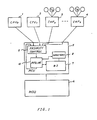
- Fig. 1 is a schematic diagram of an example of the structure of a data processing system.
- 1 and 2 are two central processing units CPU O and CPU,; 3 and 4 are four channel processing units CHP O -CHP 3 ;
- 5 is a memory control unit MCU using the pipeline system;
- 6 is a memory unit MSU;
- 7 is a buffer memory BS, for example, using a set associative system;
- 8 is a directory used for controlling the buffer memory BS;
- 9 is a priority determination circuit;
- 10 is a pipeline consisting of multistage registers.
- the MCU accepts access requests forthe MSU at any time from any of the processing, units CPU O , CPU,, CHPo-CHP3 and executes memory control based on a buffer system using the directory and buffer memory BS.
- memory control based on a buffer system means control such that the directory is searched to determine whether or not a data block in respect of which an access request has been issued is in BS; when the block exists in BS, BS is accessed, but if the block does not exist in BS, access is made to the MSU and the pertinent block is loaded into BS, thereafter access being made to BS.
- the priority determination circuit selects one access request according to a constant priority determination theory and the selected access request is executed.
- priority determination system for access requests regarding priority as between requests from CHP's and CPU's, requests from CHP's are given higher priority, while regarding priority as between one CPU and another, priority is determined in accordance with a priority determination theory determined for each unit, and an access request from the loop back (described later) should have the highest priority (Japanese laid-open patent No. 164338/1982).
- the MCU determines priority when it accepts access requests from a plurality of CHP's and CPU's and executes pipeline processing for the access requests accepted.
- a first priority determination process determines priority as between CHP's in order to select one access request therefrom, then a second priority determination process determines priority as between the selected CHP access request, access requests relating to the plurality of CPU's and loop back access requests for using the pipeline again. Thereby, one access request is selected. Thereafter, the selected access requests are sequentially input to the pipeline in order, to execute the required processing.
- a CHP access request even if it is selected on the basis of the first priority determination process, may be nullified as explained below.
- a CHP access the priority of which has been nullified in the second priority determination process may not be started again from the first priority determination process. It may be held over to obtain priority in the second priority determination process (held over so as not to compete in the first priority determining process).
- hardware is necessary for holding the access request of which the priority has been nullified and hardware is necessary for a control circuit which judges whether the waiting CHP access or successive net CHP acceses should take part in the second priority determination process.
- the access request operations which the MCU can be called upon to process include such things as block access, which require operations to be carried out a plurality of times continuously or consecutively, and loop back access request operations of comparatively low priority, such as a prefetch request, or comparatively high priority, such as error processing.
- block access which require operations to be carried out a plurality of times continuously or consecutively
- comparatively low priority such as a prefetch request
- comparatively high priority such as error processing.
- a Distributed Virtual Support Information Exchange System discloses a priority system, for controlling accesses to a common serial bus or line wherein priority allocated to an access request is dynamically changed after each unsuccessful attempt to access the line, to increase the probability of further accesses.
- US ⁇ A ⁇ 3 377 579 discloses access control apparatus on which as between I/O channels and CPU access requests, preference is given to I/O channel access requests.
- the present invention provides for determination of priority as between a plurality of access requests, and more practically provides a processing system for handling memory access requests from central processing units (CPU's) and channel processing units (CHP's) for example.
- CPU's central processing units
- CHP's channel processing units
- the priority of a CHP access request, of which the priority has once been nullified is raised when it takes part in a first priority determination process so that it can overcome (gain priority over) other CHP access requests in such priority determination, thereby to curtail even a very short period of time involved in the access processing time of a CHP access request of which the priority has once been nullified.
- An embodiment of the present invention can improve efficiency of access processing by executing priority determination between a competing plurality of access requests more carefully that has previously been the case and can provide a control system for modifying priority in accordance with the natures of different access request operations on the basis of comparatively uniform priority determination theory reset-by hardware.
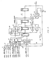
- Fig. 2, 11 is a CHP port (register), accepting addresses and control signals sent from CHP o -CHP 3 .
- 12 is a CHP selector which is controlled by CHP priority determination circuit.
- 13 is the CHP priority determination circuit, which selects one access request signal REQ from amongst access request signals REQ from CHP O -CHP 3 and then outputs the selected REQ signal (of the selected CHP-indicated as SCH) for further priority determination with regard to access requests from other access requesting units.
- the circuit 13 includes state or status indication registers provided respectively for each CHP and thereby the processing conditions of access requests from each CHP, and busy conditions of ports are indicated. Details will be explained later.
- 14 is a CPU port, accepting addresses and control signals sent from CPU O , CPU,, from the selected channel processing unit SCH and from the loop back LB.
- 15 is a CPU selector to be controlled by the main priority determination circuit 16, as explained in detail below.
- 16 is the main priority determination circuit which determines priority as between REQ signals sent from CPU o , CPU,, SCH and LB which all provide inputs to the CPU selector 15.
- a signal P ⁇ K output from the circuit 16 to the circuit 13 indicates that the SCH is not selected by the main priority determination circuit.
- 17 is a pipeline consisting of multistage register T i , T 2 , ..., T n and T,V, T 2 V, T 3 V, are validity signals of each register stage.
- 18 is a circuit having a set conflict detecting function as explained above.
- 19 is a nullification control circuit which detects a processing disable condition for a started access request and nullifies the request.
- the circuits 18 and 19 indicate a processing continuation disable (NULLIFY) condition, a validity signal inversion takes place and the execution disable signal EXEC is output.
- NULLIFY processing continuation disable
- the priority determination theory of the main priority determination circuit 16 includes two conditions:- that priority follows the sequence CPU ⁇ SCH ⁇ LB and also as between CPU's follows the indication of hot and cold flags relating thereto.
- 81 is a comparison circuit which detects whether or not wanted data exists in BS using the directory. When it exists, 81 generates an output (FOUND).
- 20 is an MSU access control circuit which sets a request to an MSU access port 21 when BS is NOT FOUND. Moreover, when the plurality of MSU ports are all busy, a signal MP BSY is supplied to the nullification control circuit 19.
- 23 is a selector which selects any one of the plurality of MSU ports 21 and sends the necessary part of the contents held in the port to the MSU.
- 24 is a selector operable to select any one of the access requests for MSU access or an access request from the final stage register Tn of the pipeline and then loops it back to the second priority determination means (main priority determination circuit).
- an access request in respect of which data is FOUND
- a block fetch request the number of bytes transferred by a single access to BS is limited to only n bytes, for example, 8 bytes, and to complete the block fetch access to BS must be effected repeatedly many times continuously or consecutively.
- Fig. 3 is an example of structure of a status indication register 13a.
- Such registers are provided in the circuit 13 in respect of each CHP in order to control CHP access requests from each CHP.
- the first bit of a status indication register is "1" (REQUEST) when an access request is issued from the relevant CHP.
- the second bit of the register is used to indicate that an access request has already been accepted, that a priority determination process is being executed and that pipeline processing is also being executed and therefore the CHP port 11 is busy (PORT BUSY).
- the third to sixth bits are used for condition codes indicating the control status of priority determination processing and pipeline processing at the port in relation to the accepted access request (ACCEPTED 0, 1, 2, 3).
- Fig. 4 illustrates transitions of status as indicated by a status indication register 13a shown in Fig. 3. A total of nine different statuses are illustrated.
- the status indication register is in a reset state with contents (000000) and when an access request REQ is accepted by the port 11, its state changes to (100000).
- first priority determination processing is carried out in the CHP priority determination circuit 13.
- the access request is selected (P)
- the state of the register changes to (110110).
- the register waits in the state (110000) until the access request is selected.
- the CHP access request selected in the CHP priority determination circuit 13 then takes part in second priority determination processing in the main priority determination circuit 16.
- the state of the status indication register changes to (110101) and when the access request is executed (EXEC), the state changes to (100100).
- EXEC access request is executed
- the register state returns to (100000). If next access request is not accepted RE ), the state returns to (000000).
- the state changes to (111011) and a higher priority may be given herein. Therefore, the access request is selected from the first phase (P(High)), the state becomes (111111) and it receives again the processing of the second phase. That is, if the CHP access request is not selected in the second priority determination process, it is given a higher priority for subsequent priority processing. Therefore, in a subsequent first priority determination process this higher priority will result in selection of the request and it will again go forward for second priority determination processing; when the access request is selected (in the second priority determination processing) (POK), the state moves to 110101) again and is executed. However, if it is not selected POK), the state returns to (111011) and selection is started again from the first priority processing phase and is repeated until the request is eventually selected in the second phase (POK).
- an embodiment of this invention provides that it is possible to execute control in such a manner that even if priority is lost in second or subsequent priority determination phases, an access request can be immediately selected when it returns to the first phase.
- Fig. 5 is a timing chart illustrating an example of the timing of operations and indicates logical conditions for generating the state transitions shown in the status indication table of Fig. 4 and control contents based on the generated status indications.
- the timing chart has horizontal levels labelled a to n.
- a indicates clock periods; E-E is the clock period of CHP.
- CPU and MCU clock periods are 1/2 of E-E.
- b indicates a port (CHP port) busy period, c indicates a port busy period in the MCU.
- d indicates a period in which an access request exists.
- e indicates the priority P or P (HIGH) period given in the first priority determination phase.
- fto i indicate state indication codes with a solid line indicating "2" and a blank indicating "0".
- n indicates the correspondence of conditions shown in Fig. 5 to statuses shown in Fig. 4.
- the circles in Fig. 5 indicate input logical conditions for starting control operations.
- Fig. 6 shows an example of internal circuitry for the CHP priority determination circuit 13.
- 131 is a 1-bit register which receives a request signal REQ from a CHP;
- 132 is a set-reset type flip-flop which receives a request signal from register 131 at its set(s) input, and outputs an internal port busy signal IPBSY which is received by a set-reset type flip-flop 133 which outputs a port busy signal PBSY;
- 134 is a register having a plurality of bits which receives operations codes from the CHP;
- 135 is a 4-bit register which holds the state indication bits ACCEPTED 0-3.
- 131, 133, 135 correspond to a state indication register 13a as shown in Fig. 3.
- 136 is a decoder which decodes the contents of indication registers 135 and determines whether priority is to be raised to high or not; 137 sends a signal PORT SEL SIG for selecting one CHP in accordance with the output of these registers and decoders, a REQ signal concerning the selected CHP (SCH) and an OP code, and simultaneously controls the state of register 135 as explained with reference to Fig. 4.
- a practical embodiment of circuit 137 can easily be designed by those who are skilled in the art, on the basis of Fig. 4 and the explanation thereof.
- the PBSY flip-flop 133 is reset by the EXEC signal (actually, there are four signals EXECO-EXEC3 corresponding to four CHP). When PBSY is reset, the IPBSY flip-flop 132 is reset.
- Fig. 7 illustrates in detail the set conflict detection circuit 18 of Fig. 2, including a plurality of address registers 181 which receive address information from the T1 stage of the pipeline and hold that information until the end of access to the buffer memory BS, a plurality of comparators 182 which compare the address information from registers 181 and the address information in the T1 stage, and OR gates 183 which OR the output of these comparators to provide a set conflict signal whenever a comparator indicates coincidence of its inputs.
- Each register 181 provides a validity bit V and its set condition is the same as that of validity bit T 2 V of the T2 stage of the pipeline. Namely, if a certain request is invalidated when it moves to T 2 , there is no need to hold the address of such request in the register 181.
- the V bit of register 181 is reset when there is desired data in the BS and its access is completed, or when there is no desired data in the BS, and an access is issued for the MSU.
- Fig. 8 illustrates in a detail the nullification control circuit 19 of Fig. 2.
- 191 is a decoder which decodes the operation OP code in the stage T, of the pipeline and discriminates a memory access request MEM from other requests MEM (for example, transfer of control data from CPU to CHP).
- T 2 V is turned ON under the condition that the there is no set conflict SET CONF and T,V is ON.
- a request MEM other than a memory access request turns ON T 2 V only with the condition of T,V.
- T 2 V can be transferred to T 3 V, but when it is NOT FOUND in. BS, the MSU access is necessary and T 2 V is transferred to T 3 V under a condition that an MSU port 21 is not busy.
- T 3 V Since there is no probability of nullification in the successive stages of T 3 , the fact that T 3 V is turned ON means that normal processing is possible in the pipeline. On the contrary, when T 3 V is turned OFF, the unexecutable signal EXEC must be notified to the CHP priority circuit. In this case, the REQ ID in the stage T 3 is decoded by the decoder 195, any of EXEC 0-3 of the corresponding CHP is output through the gate 196.
- 192,193,197,198,196 are AND gates, while 194, 199 are OR gates.
- CPU BLOCK access In the case of CPU BLOCK access, the access request appears only once but the priority is obtained for each 8-BYTE access needed to complete the block access. Namely, priority is obtained eight times in total and the processing of 1-BLOCK (64 BYTE) is completed. Therefore, CPU BLOCK access involves basically the same processing as 8-BYTE STORE an 8-BYTE access of CHP and is equivalent to executing 8-BYTE access eight times.
- the main priority determination circuit 16 is used for such processing and the algorithm in accordance with which it operates to modify priority assignments is indicated below.
- Fig. 9 is a detail block diagram of the main priority determination circuit 16.
- Fig. 9,161 is a control circuit for CPU o .
- the OP code is decoded and block access BLOCK, memory access including block access MEM and other accesses OTHER are identified.
- bank conflict is checked. Namely, it is checked whether the bank to be accessed is busy or not, using a bank address BNKADRS in the access address and a busy signal BANKBSY of each bank (not shown) of BS. When it is busy (BNK CONF), such access request is not selected.
- the circuit 162 is a control circuit for CPU1 and its operation is the same as that of the circuit 161 and therfore it is not described.
- the H/C flag is set when CPUO accessing is complete and is reset when CPU1 accessing is complete.
- the circuit 163 is the control circuit for SCH. Since a CHP allows only 8-byte accesses, the OP code is not decoded. When there is no bank conflict, REQV is ON, there is no loop back selection signal (PSELLB) and there is no CPUO or CPU1 block access the selection signal PSELSCH is turned ON. When PSELSCH turns ON, the REQ of SCH and OP code are selected and output, and the signal obtained by delaying PSELSCH by one cycle through FF2 becomes POK.
- the circuit 164 is a control circuit for loop back. This circuit identifies a prefetch access and other accesses by decoding an OP code. In the case of a prefetch access, PSELLB turns ON only when REQV of SCH is OFF and REQV of LB is ON. In the case of other accesses, PSELLB turns ON when REQV of LB is ON.
- the REQ, OP-CODE outputs from the circuits 161 to 164 are connected to the T, stage of the pipeline through the OR gate OR1, whilst PSELCPUO, PSELCPU1, PSELSCH, and PSELLB are connected to the TV bit of the T, stage through the OR gate OR2. These four PSEL signals are connected also to the selector 15 and then used for selection control.
- a CHP access request which has once obtained priority but has lost that priority for some reason is afforded opportunities for re-execution, to realize smoother processing, because it is given a higher priority than that of other CHP access requests in repeated priority determination processes.
- priority determination is carried out with careful modification in consideration of the operational contents of or significance of an access request based on the result judged from the point of view of hardware, in place of priority determination from the fixed view point of hardware, and access efficiency as a whole can be improved and moreover a total processing time in the data processing system can also be curtailed.
- the present invention relates to access request control apparatus and more specifically to apparatus for determining priority between a plurality of access requests in memory control apparatus.
- One of the access requests from a plurality of channel processing devices CHP's is selected by a first priority determination circuit, whilst one of said selected CHP request, requests from a plurality of central processing units and loop back requests from a pipeline control circuit is selected by a second priority determination circuit.
- a CHP request is not selected by the second priority determination circuit or selected but nullified in the course of pipeline processing, such a request is returned again to the first priority determination circuit. However, in this case, a higher priority is given to the request when it returns to the first priority determination circuit.
- the priority algorithm for the second priority determination circuit considers the kinds of operations involved in each access request and thereby highly efficient memory access can be realized.
Landscapes
- Engineering & Computer Science (AREA)
- Theoretical Computer Science (AREA)
- Physics & Mathematics (AREA)
- General Engineering & Computer Science (AREA)
- General Physics & Mathematics (AREA)
- Multi Processors (AREA)
- Complex Calculations (AREA)
Claims (3)
Applications Claiming Priority (4)
| Application Number | Priority Date | Filing Date | Title |
|---|---|---|---|
| JP104736/82 | 1982-06-18 | ||
| JP57104736A JPS58222361A (ja) | 1982-06-18 | 1982-06-18 | デ−タ処理システムにおけるアクセス要求の優先順位決定制御方式 |
| JP108775/82 | 1982-06-24 | ||
| JP57108775A JPS58225463A (ja) | 1982-06-24 | 1982-06-24 | アクセス処理方式 |
Publications (3)
| Publication Number | Publication Date |
|---|---|
| EP0097499A2 EP0097499A2 (de) | 1984-01-04 |
| EP0097499A3 EP0097499A3 (en) | 1985-07-31 |
| EP0097499B1 true EP0097499B1 (de) | 1989-08-23 |
Family
ID=26445142
Family Applications (1)
| Application Number | Title | Priority Date | Filing Date |
|---|---|---|---|
| EP83303505A Expired EP0097499B1 (de) | 1982-06-18 | 1983-06-17 | Zugriffsanforderungs-Steuergerät für ein Datenverarbeitungssystem |
Country Status (7)
| Country | Link |
|---|---|
| EP (1) | EP0097499B1 (de) |
| KR (1) | KR860000904B1 (de) |
| AU (1) | AU540649B2 (de) |
| BR (1) | BR8303232A (de) |
| CA (1) | CA1193024A (de) |
| DE (1) | DE3380457D1 (de) |
| ES (1) | ES8501545A1 (de) |
Families Citing this family (2)
| Publication number | Priority date | Publication date | Assignee | Title |
|---|---|---|---|---|
| US4788640A (en) * | 1986-01-17 | 1988-11-29 | Intel Corporation | Priority logic system |
| CN114281413B (zh) * | 2021-12-28 | 2025-02-07 | 海光信息技术股份有限公司 | 流水线冲突处理方法、数据处理装置、电子设备和介质 |
Family Cites Families (3)
| Publication number | Priority date | Publication date | Assignee | Title |
|---|---|---|---|---|
| GB1077339A (en) * | 1965-04-05 | 1967-07-26 | Ibm | Control device for a data processor |
| US4152764A (en) * | 1977-03-16 | 1979-05-01 | International Business Machines Corporation | Floating-priority storage control for processors in a multi-processor system |
| US4345309A (en) * | 1980-01-28 | 1982-08-17 | Digital Equipment Corporation | Relating to cached multiprocessor system with pipeline timing |
-
1983
- 1983-06-16 KR KR1019830002695A patent/KR860000904B1/ko not_active Expired
- 1983-06-17 ES ES523396A patent/ES8501545A1/es not_active Expired
- 1983-06-17 AU AU15883/83A patent/AU540649B2/en not_active Ceased
- 1983-06-17 DE DE8383303505T patent/DE3380457D1/de not_active Expired
- 1983-06-17 EP EP83303505A patent/EP0097499B1/de not_active Expired
- 1983-06-17 CA CA000430645A patent/CA1193024A/en not_active Expired
- 1983-06-17 BR BR8303232A patent/BR8303232A/pt not_active IP Right Cessation
Also Published As
| Publication number | Publication date |
|---|---|
| KR840005230A (ko) | 1984-11-05 |
| ES523396A0 (es) | 1984-12-01 |
| KR860000904B1 (ko) | 1986-07-16 |
| EP0097499A2 (de) | 1984-01-04 |
| ES8501545A1 (es) | 1984-12-01 |
| CA1193024A (en) | 1985-09-03 |
| EP0097499A3 (en) | 1985-07-31 |
| BR8303232A (pt) | 1984-01-31 |
| DE3380457D1 (en) | 1989-09-28 |
| AU1588383A (en) | 1983-12-22 |
| AU540649B2 (en) | 1984-11-29 |
Similar Documents
| Publication | Publication Date | Title |
|---|---|---|
| US4755938A (en) | Access request control apparatus which reassigns higher priority to incomplete access requests | |
| EP0057788B1 (de) | Datenverarbeitungssystem mit externem Mikrokodesteuerwerk | |
| US5293500A (en) | Parallel processing method and apparatus | |
| US6219775B1 (en) | Massively parallel computer including auxiliary vector processor | |
| US4843543A (en) | Storage control method and apparatus | |
| US4499536A (en) | Signal transfer timing control using stored data relating to operating speeds of memory and processor | |
| US4394736A (en) | Data processing system utilizing a unique two-level microcoding technique for forming microinstructions | |
| US4371925A (en) | Data processing system having unique bus control operation | |
| GB2159309A (en) | Vector processor | |
| US5898882A (en) | Method and system for enhanced instruction dispatch in a superscalar processor system utilizing independently accessed intermediate storage | |
| JPH10134008A (ja) | 半導体装置およびコンピュータシステム | |
| EP0652514B1 (de) | Datenverarbeitungsgerät zum Behandeln von mehreren, geteilten Unterbrechungen | |
| EP0125855A2 (de) | Steuerungssystem für Pufferspeicher | |
| US4048623A (en) | Data processing system | |
| JP3400458B2 (ja) | 情報処理装置 | |
| US5710914A (en) | Digital signal processing method and system implementing pipelined read and write operations | |
| EP0035334A2 (de) | Datenverarbeitungssystem mit Zweiebenen-Mikroprogrammierung | |
| US4755931A (en) | Vector processing unit capable of reading vector data from a vector register simultaneously to plural resources | |
| EP0223150B1 (de) | Informationsverarbeitungsvorrichtung | |
| US4236205A (en) | Access-time reduction control circuit and process for digital storage devices | |
| EP0097499B1 (de) | Zugriffsanforderungs-Steuergerät für ein Datenverarbeitungssystem | |
| EP0309330A2 (de) | Prioritätszugriffssteuerungssystem zum Hauptspeicher für Rechner | |
| US5889966A (en) | Data processor having bus controller for controlling a plurality of buses independently of each other | |
| US4464772A (en) | Frequency synthesizer for providing a pseudo-constant frequency signal | |
| EP0573071A2 (de) | Mikroprozessor |
Legal Events
| Date | Code | Title | Description |
|---|---|---|---|
| PUAI | Public reference made under article 153(3) epc to a published international application that has entered the european phase |
Free format text: ORIGINAL CODE: 0009012 |
|
| AK | Designated contracting states |
Designated state(s): DE FR GB |
|
| PUAL | Search report despatched |
Free format text: ORIGINAL CODE: 0009013 |
|
| AK | Designated contracting states |
Designated state(s): DE FR GB |
|
| 17P | Request for examination filed |
Effective date: 19851125 |
|
| 17Q | First examination report despatched |
Effective date: 19871119 |
|
| GRAA | (expected) grant |
Free format text: ORIGINAL CODE: 0009210 |
|
| AK | Designated contracting states |
Kind code of ref document: B1 Designated state(s): DE FR GB |
|
| REF | Corresponds to: |
Ref document number: 3380457 Country of ref document: DE Date of ref document: 19890928 |
|
| ET | Fr: translation filed | ||
| PLBE | No opposition filed within time limit |
Free format text: ORIGINAL CODE: 0009261 |
|
| STAA | Information on the status of an ep patent application or granted ep patent |
Free format text: STATUS: NO OPPOSITION FILED WITHIN TIME LIMIT |
|
| 26N | No opposition filed | ||
| PGFP | Annual fee paid to national office [announced via postgrant information from national office to epo] |
Ref country code: FR Payment date: 19990610 Year of fee payment: 17 |
|
| PGFP | Annual fee paid to national office [announced via postgrant information from national office to epo] |
Ref country code: GB Payment date: 19990616 Year of fee payment: 17 |
|
| PGFP | Annual fee paid to national office [announced via postgrant information from national office to epo] |
Ref country code: DE Payment date: 19990618 Year of fee payment: 17 |
|
| PG25 | Lapsed in a contracting state [announced via postgrant information from national office to epo] |
Ref country code: GB Free format text: LAPSE BECAUSE OF NON-PAYMENT OF DUE FEES Effective date: 20000617 |
|
| GBPC | Gb: european patent ceased through non-payment of renewal fee |
Effective date: 20000617 |
|
| PG25 | Lapsed in a contracting state [announced via postgrant information from national office to epo] |
Ref country code: FR Free format text: LAPSE BECAUSE OF NON-PAYMENT OF DUE FEES Effective date: 20010228 |
|
| REG | Reference to a national code |
Ref country code: FR Ref legal event code: ST |
|
| PG25 | Lapsed in a contracting state [announced via postgrant information from national office to epo] |
Ref country code: DE Free format text: LAPSE BECAUSE OF NON-PAYMENT OF DUE FEES Effective date: 20010403 |