EP0097819A1 - Photo-dépôt des métaux sur substrats - Google Patents
Photo-dépôt des métaux sur substrats Download PDFInfo
- Publication number
- EP0097819A1 EP0097819A1 EP83105173A EP83105173A EP0097819A1 EP 0097819 A1 EP0097819 A1 EP 0097819A1 EP 83105173 A EP83105173 A EP 83105173A EP 83105173 A EP83105173 A EP 83105173A EP 0097819 A1 EP0097819 A1 EP 0097819A1
- Authority
- EP
- European Patent Office
- Prior art keywords
- substrate
- metal
- onto
- tungsten
- vicinity
- Prior art date
- Legal status (The legal status is an assumption and is not a legal conclusion. Google has not performed a legal analysis and makes no representation as to the accuracy of the status listed.)
- Granted
Links
Images
Classifications
-
- H—ELECTRICITY
- H10—SEMICONDUCTOR DEVICES; ELECTRIC SOLID-STATE DEVICES NOT OTHERWISE PROVIDED FOR
- H10D—INORGANIC ELECTRIC SEMICONDUCTOR DEVICES
- H10D64/00—Electrodes of devices having potential barriers
- H10D64/01—Manufacture or treatment
- H10D64/012—Manufacture or treatment of electrodes comprising a Schottky barrier to a semiconductor
- H10D64/0124—Manufacture or treatment of electrodes comprising a Schottky barrier to a semiconductor to Group III-V semiconductors
-
- C—CHEMISTRY; METALLURGY
- C23—COATING METALLIC MATERIAL; COATING MATERIAL WITH METALLIC MATERIAL; CHEMICAL SURFACE TREATMENT; DIFFUSION TREATMENT OF METALLIC MATERIAL; COATING BY VACUUM EVAPORATION, BY SPUTTERING, BY ION IMPLANTATION OR BY CHEMICAL VAPOUR DEPOSITION, IN GENERAL; INHIBITING CORROSION OF METALLIC MATERIAL OR INCRUSTATION IN GENERAL
- C23C—COATING METALLIC MATERIAL; COATING MATERIAL WITH METALLIC MATERIAL; SURFACE TREATMENT OF METALLIC MATERIAL BY DIFFUSION INTO THE SURFACE, BY CHEMICAL CONVERSION OR SUBSTITUTION; COATING BY VACUUM EVAPORATION, BY SPUTTERING, BY ION IMPLANTATION OR BY CHEMICAL VAPOUR DEPOSITION, IN GENERAL
- C23C16/00—Chemical coating by decomposition of gaseous compounds, without leaving reaction products of surface material in the coating, i.e. chemical vapour deposition [CVD] processes
- C23C16/06—Chemical coating by decomposition of gaseous compounds, without leaving reaction products of surface material in the coating, i.e. chemical vapour deposition [CVD] processes characterised by the deposition of metallic material
- C23C16/16—Chemical coating by decomposition of gaseous compounds, without leaving reaction products of surface material in the coating, i.e. chemical vapour deposition [CVD] processes characterised by the deposition of metallic material from metal carbonyl compounds
-
- C—CHEMISTRY; METALLURGY
- C23—COATING METALLIC MATERIAL; COATING MATERIAL WITH METALLIC MATERIAL; CHEMICAL SURFACE TREATMENT; DIFFUSION TREATMENT OF METALLIC MATERIAL; COATING BY VACUUM EVAPORATION, BY SPUTTERING, BY ION IMPLANTATION OR BY CHEMICAL VAPOUR DEPOSITION, IN GENERAL; INHIBITING CORROSION OF METALLIC MATERIAL OR INCRUSTATION IN GENERAL
- C23C—COATING METALLIC MATERIAL; COATING MATERIAL WITH METALLIC MATERIAL; SURFACE TREATMENT OF METALLIC MATERIAL BY DIFFUSION INTO THE SURFACE, BY CHEMICAL CONVERSION OR SUBSTITUTION; COATING BY VACUUM EVAPORATION, BY SPUTTERING, BY ION IMPLANTATION OR BY CHEMICAL VAPOUR DEPOSITION, IN GENERAL
- C23C16/00—Chemical coating by decomposition of gaseous compounds, without leaving reaction products of surface material in the coating, i.e. chemical vapour deposition [CVD] processes
- C23C16/44—Chemical coating by decomposition of gaseous compounds, without leaving reaction products of surface material in the coating, i.e. chemical vapour deposition [CVD] processes characterised by the method of coating
- C23C16/48—Chemical coating by decomposition of gaseous compounds, without leaving reaction products of surface material in the coating, i.e. chemical vapour deposition [CVD] processes characterised by the method of coating by irradiation, e.g. photolysis, radiolysis, particle radiation
- C23C16/483—Chemical coating by decomposition of gaseous compounds, without leaving reaction products of surface material in the coating, i.e. chemical vapour deposition [CVD] processes characterised by the method of coating by irradiation, e.g. photolysis, radiolysis, particle radiation using coherent light, UV to IR, e.g. lasers
Definitions
- the invention relates to photodeposition of refractory metals onto substrates.
- refractory metal such as Cr, Mo, and W were deposited using laser-induced gas phase photolysis of hexacarbonyl compounds of these metals.
- Clusters of metal crystallites were formed on a substrate when the laser beam was focussed, while threads of metal crystallites were formed when the laser beam was defocussed.
- the prior art does not recognize the superior results which can be obtained with lower wavelength ultraviolet radiation and carbonyl compounds.
- the Solanki et al reference teaches the use of longer wavelength ultraviolet light with hexacarbonyl compounds for the deposition of refractory metals. At longer wavelengths, the carbonyls do not photodecompose to metal, a heat effect also being required to decompose the hexacarbonyls to free metal atoms.
- the prior art does not recognize that wavelengths less than 200 nm can be used with carbonyls to give superior metal deposition. The use of wavelengths less than 200 nm is also advantageous in that focussed ultraviolet beams are not required. This means that heat buildup at the substrate can be avoided.
- GaAs is a semiconductor material which has properties that are advantageous with respect to the properties of other semiconductor materials, such as silicon.
- GaAs has higher mobility than Si, and less resistance.
- GaAs is not easily oxidized or metallized, which is a disadvantage to its employment in a variety of device structures.
- tungsten gate electrodes have been applied to GaAs MESFETs by sputtering and ebeam evaporation. In both of these processes, damage occurs to the GaAs surface. Sputtering causes impact damage, and ebeam evaporation results in dissociation of GaAs.
- the present invention is also useful in the fabrication of other devices where surface damage may be caused by metal deposition techniques such as evaporation and sputtering.
- metal deposition techniques such as evaporation and sputtering.
- solar cells often use tungsten contacts, but surface damage has to be avoided.
- This invention is a process for photodeposition of a refractory metal from a gaseous carbonyl compound including the refractory metal.
- Photodeposition occurs when ultraviolet radiation of wavelengths less than 200 nm strikes the gaseous carbonyl compounds in the vicinity of the substrate. Continuous layers of metal are deposited on the substrate in those regions adjacent to where the ultraviolet radiation strikes the carbonyl compounds.
- the substrate can be any type of material, including but not restricted to quartz, glass, semiconductors such as Si and GaAs, polymers, and metals. In a particularly important embodiment, layers of tungsten are photodeposited onto GaAs.
- the invention provides a method for photodeposition of a refractory metal onto a substrate, comprising the steps of producing a carbonyl compound vapor of said metal in the vicinity of a substrate, directing ultraviolet light of wavelengths less than 200 nm onto said vapour to photodecompose said vapour to release atoms of said metal in the vicinity of or on said substrate, and condensing said metal atoms onto said substrate to form a continuous refractory metal layer thereon.
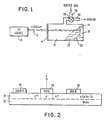
- FIG. 1 shows a suitable apparatus for carrying out the process of the present invention.
- an ultraviolet light source 10 provides an output beam of radiation 12 having wavelengths less than 200 nm. Beam 12 passes through a fused silica window 14 of the chamber 16, and travels to the vicinity of the substrate 18, in front of which is a mask 19.
- Located inside chamber 16 is a source of refractory metal carbonyl vapours 20, the source being, for example, metal carbonyl powder 22.
- Chamber 16 is also provided with an input/output port 24, in which a valve 26 is located.
- a buffer gas, such as helium, can be introduced into chamber 16 via inlet 28, while a vacuum can be produced in chamber 16 by exhausting the atmosphere therein through outlet pipe 30.
- Source 10 provides ultraviolet radiation having wavelengths less than 200 nm, and can be a source providing pulsed outputs or continuous wave outputs.
- An example of a pulsed output source is an ArF excimer laser which will produce output pulses of approximately 10 nsec width'at 193 nm.
- a continuous wave source suitable for the present invention is a low pressure mercury vapour lamp providing a continuous output at 185 nm. Both of the sources are commercially available.
- the input ultraviolet radiation beam 12 passes through window 14 and strikes the vapours 20 inside reaction chamber 16. Molecular bonds of the vapour near and/or adsorbed on substrate 18 are broken by the photons in the ultraviolet radiation and produce free metal atoms. The atoms in the vicinity of substrate 18 condense on the substrate. The particular pattern of metal deposited on substrate 18 is defined by the radiation beam 12.
- scanning beam 12 deposition can be made to occur on different portions of substrate 18.
- beam 12 is often collimated and focussed by optical apparatus, including focussing lenses.
- the light beam 12 can also be patterned by projection through a mask, such as mask 19 in FIG. 1.
- a metal carbonyl compound in the form of a powder 22 is placed on the bottom of the reaction chamber 16.
- Chamber 16 is then pumped down by a pump (not shown).
- Chamber 16 can be back filled with a buffer gas, such as He, in order to reduce the mean free path of the free metal atoms. This confines the metal photofragments to the small regions immediately surrounding the volume of input beam 12.
- a heater (not shown) can also be provided to heat reaction chamber 16, and specifically powder 22, in order to increase the metal carbonyl vapour pressure in chamber 16.
- the temperature in the reaction chamber is kept below a temperature where thermodecomposition of the metal carbonyl vapours would occur.
- the gas pressures within reaction chamber 16 are not critical, and can range from pressures less than 10 Torr to about 3 Torr of the refractory metal carbonyl vapour and about 750 Torr He.
- the exposure times of the carbonyl vapours to the ultraviolet beam 12 can typically range from less than 1 second to several seconds or minutes. The exposure time depends upon the density of the metal carbonyl vapour and the required thickness of the metal deposit.
- the use of a laser beam allows ready spatial localization of the reaction region, and may be focussed to provide high resolution patterns on the substrate. Because the metal carbonyl vapour has a very high absorption for light at the specified wavelength range, there is very little, if any, heating of the substrate. Also, the deposited film does not ablate due to the light beam. Since a mask 19 can be used, the light beam need not be focussed, and therefore adverse heating of the substrate or deposited metal can be avoided.
- the light source 10 can be either a continuous wave source or a pulsed source, as noted previously. For some applications, such as those requiring large area depositions (for example, projection printing of a mask), pulsed sources may be more appropriate, due to the average powers which can be obtained with them. For direct writing applications, a scanned focussed cw laser may be more appropriate.
- Use of a buffer gas in the reaction chamber 16 helps to confine the mean free path of the metal atoms, and therefore provides more localized depositon. However, the addition of the buffer gas may sometimes affect the deposition rate.
- the pressures of the metal carbonyl vapours and the buffer gas are not critical, nor is the temperature within the reaction chamber 16 and at the substrate 18. Room temperatures are suitable.
- FIG. 2 shows a GaAs MESFET (metal electrode semiconductor field effect device) which is comprised of a layer 32 of semiinsulating GaAs, a layer 34 of ntype GaAs-Si, source and drain electrodes 36, 38 respectively, and a metal gate electrode 40.
- Gate electrode 40 is tungsten, which makes a Schottky barrier diode where it contacts the underlying semiconductor layer 34. In the operation of this device, current flows from the source 36 to the drain 38 in accordance with the applied voltage V at the gate electrode 40.
- the preferred gate electrode material is tungsten because it has a high Schottky barrier with semiconductor layer 34, and because it will not alloy with GaAs in the high temperature (800900°C) process typically used in fabrication. Other metals, such as Au, Al, etc. will alloy with GaAs and produce ohmic contacts rather than diode barriers. Tungsten also has another desirable characteristic because it functions as a mask when the n + regions are prepared by diffusion.
- the tungsten gate electrode 40 can be deposited by the method of the present invention. This will not cause any type of damage to semiconductor layer 34 and can be done at a low temperature « 30°C) because wavelengths less than 200 nm photodecompose the tungsten hexacarbonyl W(CO) 6 . This hexacarbonyl decomposes with ultraviolet radiation at an electronically excited state, rather than a thermally activated or ionized state.
- the specific process steps for the fabrication of the device in FIG. 2 are the following:
- tungsten was deposited on a high resistivity GaAs wafer in the reaction chamber 16.
- Tungsten hexacarbonyl powder was used to provide the tungsten hexacarbonyl vapours in the vicinity of the GaAs wafer substrate.
- the light source was an ArF excimer laser providing ultraviolet light at 193 nm. This laser produced pulses of radiation of approximately 12 nsec duration. An exposure of 200 pulses, where each pulse was 27 mV, was made to deposit a tungsten layer by photodeposition.
- the pressure in the reaction chamber was 1 Torr, and the temperature was ambient room temperature.
- a metallic tungsten deposit having the size and shape of the ultraviolet beam was formed, a the deposit being 800 thick. It was a continuous film providing good electrical conduction.
- Mo and Cr continuous films were also photodeposited by the method of this invention.
- the conditions used for those depositions were essentially identical to those used for the tungsten deposition.
- photodeposition of refractory metals onto a substrate is achieved by combining ultraviolet excitation of carbonyl vapours of these refractory metals, using wavelengths less than 200 nm. While those of skill in the art may recognize variations that can be made in the subject process, these variations will be consistent with the principles wherein carbonyl vapours are used in combination with short wavelength ultraviolet radiation in the specified range, in order to produce superior results.
Landscapes
- Chemical & Material Sciences (AREA)
- Metallurgy (AREA)
- Chemical Kinetics & Catalysis (AREA)
- Engineering & Computer Science (AREA)
- Materials Engineering (AREA)
- Mechanical Engineering (AREA)
- General Chemical & Material Sciences (AREA)
- Organic Chemistry (AREA)
- Physics & Mathematics (AREA)
- Optics & Photonics (AREA)
- Health & Medical Sciences (AREA)
- Toxicology (AREA)
- Chemical Vapour Deposition (AREA)
- Electrodes Of Semiconductors (AREA)
Applications Claiming Priority (2)
| Application Number | Priority Date | Filing Date | Title |
|---|---|---|---|
| US06/393,998 US4451503A (en) | 1982-06-30 | 1982-06-30 | Photo deposition of metals with far UV radiation |
| US393998 | 1982-06-30 |
Publications (2)
| Publication Number | Publication Date |
|---|---|
| EP0097819A1 true EP0097819A1 (fr) | 1984-01-11 |
| EP0097819B1 EP0097819B1 (fr) | 1986-04-02 |
Family
ID=23557111
Family Applications (1)
| Application Number | Title | Priority Date | Filing Date |
|---|---|---|---|
| EP83105173A Expired EP0097819B1 (fr) | 1982-06-30 | 1983-05-25 | Photo-dépôt des métaux sur substrats |
Country Status (4)
| Country | Link |
|---|---|
| US (1) | US4451503A (fr) |
| EP (1) | EP0097819B1 (fr) |
| JP (1) | JPS599164A (fr) |
| DE (1) | DE3362768D1 (fr) |
Cited By (7)
| Publication number | Priority date | Publication date | Assignee | Title |
|---|---|---|---|---|
| EP0169485A3 (en) * | 1984-07-17 | 1988-01-27 | Nec Corporation | Method and apparatus for inducing photochemical reaction |
| EP0182193B1 (fr) | 1984-11-19 | 1988-07-06 | International Business Machines Corporation | Procédé de dépôt d'un motif en cuivre sur un support |
| GB2200138A (en) * | 1984-07-26 | 1988-07-27 | Japan Res Dev Corp | Semiconductor crystal growth apparatus |
| EP0241873A3 (en) * | 1986-04-18 | 1989-12-27 | American Telephone And Telegraph Company | Fabrication of semiconductor devices utilizing patterned metal layers |
| EP0241190A3 (fr) * | 1986-04-09 | 1990-04-04 | Massachusetts Institute Of Technology | Méthode et dispositif pour le dépôt photochimique de films sur des surfaces |
| EP0247714A3 (en) * | 1986-05-29 | 1990-12-05 | Seiko Instruments Inc. | Method and apparatus for forming a film on a substrate |
| GB2250751A (en) * | 1990-08-24 | 1992-06-17 | Kawasaki Heavy Ind Ltd | Process for the production of dielectric thin films; pyroelectric sensor |
Families Citing this family (28)
| Publication number | Priority date | Publication date | Assignee | Title |
|---|---|---|---|---|
| DE3300449A1 (de) * | 1983-01-08 | 1984-07-12 | Philips Patentverwaltung Gmbh, 2000 Hamburg | Verfahren zur herstellung einer elektrode fuer eine hochdruckgasentladungslampe |
| US6784033B1 (en) | 1984-02-15 | 2004-08-31 | Semiconductor Energy Laboratory Co., Ltd. | Method for the manufacture of an insulated gate field effect semiconductor device |
| JPS60211076A (ja) * | 1984-04-05 | 1985-10-23 | Fuji Electric Corp Res & Dev Ltd | 多層導電膜パタ−ンの形成方法 |
| US4543270A (en) * | 1984-06-20 | 1985-09-24 | Gould Inc. | Method for depositing a micron-size metallic film on a transparent substrate utilizing a visible laser |
| JPH0630339B2 (ja) * | 1984-07-16 | 1994-04-20 | 新技術事業団 | GaAs単結晶の製造方法 |
| JPH0766906B2 (ja) * | 1984-07-26 | 1995-07-19 | 新技術事業団 | GaAsエピタキシャル成長方法 |
| JPS6193830A (ja) * | 1984-10-15 | 1986-05-12 | Nec Corp | 光気相成長法 |
| JPH0752718B2 (ja) * | 1984-11-26 | 1995-06-05 | 株式会社半導体エネルギー研究所 | 薄膜形成方法 |
| US6786997B1 (en) | 1984-11-26 | 2004-09-07 | Semiconductor Energy Laboratory Co., Ltd. | Plasma processing apparatus |
| JPH0772353B2 (ja) * | 1985-08-23 | 1995-08-02 | 日本電信電話株式会社 | 薄膜堆積方法および装置 |
| JPS6245035A (ja) * | 1985-08-23 | 1987-02-27 | Hitachi Ltd | 半導体装置の製造装置 |
| US6230650B1 (en) | 1985-10-14 | 2001-05-15 | Semiconductor Energy Laboratory Co., Ltd. | Microwave enhanced CVD system under magnetic field |
| US6673722B1 (en) | 1985-10-14 | 2004-01-06 | Semiconductor Energy Laboratory Co., Ltd. | Microwave enhanced CVD system under magnetic field |
| KR910003742B1 (ko) * | 1986-09-09 | 1991-06-10 | 세미콘덕터 에너지 라보라터리 캄파니 리미티드 | Cvd장치 |
| US5427824A (en) * | 1986-09-09 | 1995-06-27 | Semiconductor Energy Laboratory Co., Ltd. | CVD apparatus |
| US4814294A (en) * | 1987-07-30 | 1989-03-21 | Allied-Signal Inc. | Method of growing cobalt silicide films by chemical vapor deposition |
| EP0365754B1 (fr) * | 1988-10-28 | 1994-11-09 | International Business Machines Corporation | Ablation par laser ultraviolet et gravure de solides organiques |
| EP0637057B1 (fr) * | 1993-07-30 | 1996-12-11 | International Business Machines Corporation | Méthode et appareil pour déposer des lignes fine de métal sur un substrat |
| US6159641A (en) * | 1993-12-16 | 2000-12-12 | International Business Machines Corporation | Method for the repair of defects in lithographic masks |
| US5789312A (en) * | 1996-10-30 | 1998-08-04 | International Business Machines Corporation | Method of fabricating mid-gap metal gates compatible with ultra-thin dielectrics |
| US6452276B1 (en) | 1998-04-30 | 2002-09-17 | International Business Machines Corporation | Ultra thin, single phase, diffusion barrier for metal conductors |
| US6248658B1 (en) | 1999-01-13 | 2001-06-19 | Advanced Micro Devices, Inc. | Method of forming submicron-dimensioned metal patterns |
| WO2001046304A2 (fr) * | 1999-12-23 | 2001-06-28 | Mobius Technologies, Inc. | Techniques de traitement de poudre de mousse polymerique, produits de poudre de mousse, et mousses contenant ces poudres de mousse |
| US6656539B1 (en) * | 2000-11-13 | 2003-12-02 | International Business Machines Corporation | Method and apparatus for performing laser CVD |
| MY145695A (en) * | 2001-01-24 | 2012-03-30 | Nichia Corp | Light emitting diode, optical semiconductor device, epoxy resin composition suited for optical semiconductor device, and method for manufacturing the same |
| JP2002294456A (ja) * | 2001-03-30 | 2002-10-09 | Oki Electric Ind Co Ltd | 膜の形成方法及びその方法を実施するためのcvd装置 |
| US11932929B2 (en) * | 2017-08-21 | 2024-03-19 | George Edward Parris | Method and materials for creating patterns of carbon and/or other elements on substrates or within liquid or frozen media by directed energy deposition of carbon and other elements |
| US20230279544A1 (en) | 2020-09-03 | 2023-09-07 | Tcm Research Ltd. | Additive chemical vapor deposition methods and systems |
Citations (3)
| Publication number | Priority date | Publication date | Assignee | Title |
|---|---|---|---|---|
| GB1067803A (en) * | 1964-04-27 | 1967-05-03 | Varian Associates | Improvements in or relating to the treating of materials by laser beam |
| US3808035A (en) * | 1970-12-09 | 1974-04-30 | M Stelter | Deposition of single or multiple layers on substrates from dilute gas sweep to produce optical components, electro-optical components, and the like |
| US4330570A (en) * | 1981-04-24 | 1982-05-18 | The United States Of America As Represented By The Secretary Of The Navy | Selective photoinduced condensation technique for producing semiconducting compounds |
Family Cites Families (4)
| Publication number | Priority date | Publication date | Assignee | Title |
|---|---|---|---|---|
| US3253946A (en) * | 1960-08-11 | 1966-05-31 | Ethyl Corp | Vapor plating with manganese, chromium, molybdenum or tungsten employing cyclopentadienyl metal carbonyl |
| US4324854A (en) * | 1980-03-03 | 1982-04-13 | California Institute Of Technology | Deposition of metal films and clusters by reactions of compounds with low energy electrons on surfaces |
| US4340617A (en) * | 1980-05-19 | 1982-07-20 | Massachusetts Institute Of Technology | Method and apparatus for depositing a material on a surface |
| JPS6021224B2 (ja) * | 1980-10-08 | 1985-05-25 | 日本電気株式会社 | レーザー薄膜形成装置 |
-
1982
- 1982-06-30 US US06/393,998 patent/US4451503A/en not_active Expired - Lifetime
-
1983
- 1983-04-14 JP JP58064649A patent/JPS599164A/ja active Pending
- 1983-05-25 DE DE8383105173T patent/DE3362768D1/de not_active Expired
- 1983-05-25 EP EP83105173A patent/EP0097819B1/fr not_active Expired
Patent Citations (3)
| Publication number | Priority date | Publication date | Assignee | Title |
|---|---|---|---|---|
| GB1067803A (en) * | 1964-04-27 | 1967-05-03 | Varian Associates | Improvements in or relating to the treating of materials by laser beam |
| US3808035A (en) * | 1970-12-09 | 1974-04-30 | M Stelter | Deposition of single or multiple layers on substrates from dilute gas sweep to produce optical components, electro-optical components, and the like |
| US4330570A (en) * | 1981-04-24 | 1982-05-18 | The United States Of America As Represented By The Secretary Of The Navy | Selective photoinduced condensation technique for producing semiconducting compounds |
Non-Patent Citations (3)
| Title |
|---|
| APPLIED PHYSICS LETTERS, vol. 35, no. 2, July 15, 1979 T.F. DEUTSCH et al. "Laser photodeposition of metal films with micropscopic features" pages 175-177 * Especially page 175, column 2 - page 176, column 1 ; page 177, lines 8-25 * * |
| APPLIED PHYSICS LETTERS, vol. 38, no. 7, April 1, 1981 R. SOLANKI et al. "Laser photodeposition of refractory metals" pages 572-574 * Especiallly page 572, column 2 - page 573, column 1 * * |
| PATENT ABSTRACTS OF JAPAN, unexamined applications, C field, vol. 5, no. 16, January 30, 1981 THE PATENT OFFICE JAPANESE GOVERNMENT, page 155 C 41 * JP - A - 55-145 178 ( KOGYO GIJUTSUIN ) * * |
Cited By (9)
| Publication number | Priority date | Publication date | Assignee | Title |
|---|---|---|---|---|
| EP0169485A3 (en) * | 1984-07-17 | 1988-01-27 | Nec Corporation | Method and apparatus for inducing photochemical reaction |
| GB2200138A (en) * | 1984-07-26 | 1988-07-27 | Japan Res Dev Corp | Semiconductor crystal growth apparatus |
| GB2200138B (en) * | 1984-07-26 | 1989-05-10 | Japan Res Dev Corp | Semiconductor crystal growth apparatus |
| EP0182193B1 (fr) | 1984-11-19 | 1988-07-06 | International Business Machines Corporation | Procédé de dépôt d'un motif en cuivre sur un support |
| EP0241190A3 (fr) * | 1986-04-09 | 1990-04-04 | Massachusetts Institute Of Technology | Méthode et dispositif pour le dépôt photochimique de films sur des surfaces |
| EP0241873A3 (en) * | 1986-04-18 | 1989-12-27 | American Telephone And Telegraph Company | Fabrication of semiconductor devices utilizing patterned metal layers |
| EP0247714A3 (en) * | 1986-05-29 | 1990-12-05 | Seiko Instruments Inc. | Method and apparatus for forming a film on a substrate |
| GB2250751A (en) * | 1990-08-24 | 1992-06-17 | Kawasaki Heavy Ind Ltd | Process for the production of dielectric thin films; pyroelectric sensor |
| GB2250751B (en) * | 1990-08-24 | 1995-04-12 | Kawasaki Heavy Ind Ltd | Process for the production of dielectric thin films |
Also Published As
| Publication number | Publication date |
|---|---|
| EP0097819B1 (fr) | 1986-04-02 |
| DE3362768D1 (en) | 1986-05-07 |
| JPS599164A (ja) | 1984-01-18 |
| US4451503A (en) | 1984-05-29 |
Similar Documents
| Publication | Publication Date | Title |
|---|---|---|
| EP0097819B1 (fr) | Photo-dépôt des métaux sur substrats | |
| US5459098A (en) | Maskless laser writing of microscopic metallic interconnects | |
| US4615904A (en) | Maskless growth of patterned films | |
| US4608117A (en) | Maskless growth of patterned films | |
| EP0456479B1 (fr) | Procédé de formation de motifs et procédé de fabrication de dispositifs semi-conducteurs utilisant de tels motifs | |
| US4340617A (en) | Method and apparatus for depositing a material on a surface | |
| US4948623A (en) | Method of chemical vapor deposition of copper, silver, and gold using a cyclopentadienyl/metal complex | |
| JPS60254614A (ja) | 光誘導による導電性ケイ化チタンフイルムの化学蒸着法 | |
| JPH0454372B2 (fr) | ||
| JPS60236219A (ja) | プラズマ生成したソースガスを用いた蒸着方法 | |
| JPS61280621A (ja) | 光化学的パタ−ン化方式 | |
| EP0241873B1 (fr) | Fabrication de dispositifs à semi-conducteur en utilisant comme patrons des couches métalliques | |
| EP0466320B1 (fr) | Procédé de préparation d'un dispositif semi-conducteur comprenant le dépôt sélectif de métal | |
| Ishihara et al. | Laser-assisted chemical vapor deposition of titanium nitride films | |
| Oprysko et al. | Nucleation effects in visible‐laser chemical vapor deposition | |
| JPS63224233A (ja) | 表面処理方法 | |
| Foulon et al. | Laser projection patterned processing of semiconductors | |
| Auvert | Kinetics and mechanisms of CW laser induced deposition of metals for microelectronics | |
| Micheli et al. | Laser microfabrication of thin films: Part three | |
| JPS61140176A (ja) | 半導体装置 | |
| EP0248883B1 (fr) | Procede de depot selectif | |
| Sugioka et al. | Selective deposition of Au films on GaAs by projection-patterned excimer laser doping combined with electroless plating | |
| Shaver et al. | Production applications of laser microchemistry | |
| Osgood Jr | An Overview of Laser Chemical Processing | |
| Boyd | Recent advances in laser processing of microelectronic materials and devices |
Legal Events
| Date | Code | Title | Description |
|---|---|---|---|
| PUAI | Public reference made under article 153(3) epc to a published international application that has entered the european phase |
Free format text: ORIGINAL CODE: 0009012 |
|
| AK | Designated contracting states |
Designated state(s): DE FR GB |
|
| 17P | Request for examination filed |
Effective date: 19840426 |
|
| GRAA | (expected) grant |
Free format text: ORIGINAL CODE: 0009210 |
|
| AK | Designated contracting states |
Kind code of ref document: B1 Designated state(s): DE FR GB |
|
| REF | Corresponds to: |
Ref document number: 3362768 Country of ref document: DE Date of ref document: 19860507 |
|
| ET | Fr: translation filed | ||
| PLBE | No opposition filed within time limit |
Free format text: ORIGINAL CODE: 0009261 |
|
| STAA | Information on the status of an ep patent application or granted ep patent |
Free format text: STATUS: NO OPPOSITION FILED WITHIN TIME LIMIT |
|
| 26N | No opposition filed | ||
| PGFP | Annual fee paid to national office [announced via postgrant information from national office to epo] |
Ref country code: GB Payment date: 19930427 Year of fee payment: 11 |
|
| PGFP | Annual fee paid to national office [announced via postgrant information from national office to epo] |
Ref country code: DE Payment date: 19930525 Year of fee payment: 11 |
|
| PGFP | Annual fee paid to national office [announced via postgrant information from national office to epo] |
Ref country code: FR Payment date: 19940427 Year of fee payment: 12 |
|
| PG25 | Lapsed in a contracting state [announced via postgrant information from national office to epo] |
Ref country code: GB Effective date: 19940525 |
|
| GBPC | Gb: european patent ceased through non-payment of renewal fee |
Effective date: 19940525 |
|
| PG25 | Lapsed in a contracting state [announced via postgrant information from national office to epo] |
Ref country code: DE Effective date: 19950201 |
|
| PG25 | Lapsed in a contracting state [announced via postgrant information from national office to epo] |
Ref country code: FR Effective date: 19960229 |
|
| REG | Reference to a national code |
Ref country code: FR Ref legal event code: ST |
|
| REG | Reference to a national code |
Ref country code: FR Ref legal event code: ST |