EP0097866B1 - Procédé de fabrication d'un dispositif semi-conducteur à région de base ayant une partie profonde - Google Patents
Procédé de fabrication d'un dispositif semi-conducteur à région de base ayant une partie profonde Download PDFInfo
- Publication number
- EP0097866B1 EP0097866B1 EP83105802A EP83105802A EP0097866B1 EP 0097866 B1 EP0097866 B1 EP 0097866B1 EP 83105802 A EP83105802 A EP 83105802A EP 83105802 A EP83105802 A EP 83105802A EP 0097866 B1 EP0097866 B1 EP 0097866B1
- Authority
- EP
- European Patent Office
- Prior art keywords
- window
- layer
- wafer
- mask layer
- invention according
- Prior art date
- Legal status (The legal status is an assumption and is not a legal conclusion. Google has not performed a legal analysis and makes no representation as to the accuracy of the status listed.)
- Expired - Lifetime
Links
Images



Classifications
-
- H—ELECTRICITY
- H10—SEMICONDUCTOR DEVICES; ELECTRIC SOLID-STATE DEVICES NOT OTHERWISE PROVIDED FOR
- H10D—INORGANIC ELECTRIC SEMICONDUCTOR DEVICES
- H10D30/00—Field-effect transistors [FET]
- H10D30/60—Insulated-gate field-effect transistors [IGFET]
- H10D30/64—Double-diffused metal-oxide semiconductor [DMOS] FETs
- H10D30/66—Vertical DMOS [VDMOS] FETs
-
- H—ELECTRICITY
- H10—SEMICONDUCTOR DEVICES; ELECTRIC SOLID-STATE DEVICES NOT OTHERWISE PROVIDED FOR
- H10D—INORGANIC ELECTRIC SEMICONDUCTOR DEVICES
- H10D12/00—Bipolar devices controlled by the field effect, e.g. insulated-gate bipolar transistors [IGBT]
- H10D12/411—Insulated-gate bipolar transistors [IGBT]
- H10D12/441—Vertical IGBTs
-
- H—ELECTRICITY
- H10—SEMICONDUCTOR DEVICES; ELECTRIC SOLID-STATE DEVICES NOT OTHERWISE PROVIDED FOR
- H10D—INORGANIC ELECTRIC SEMICONDUCTOR DEVICES
- H10D62/00—Semiconductor bodies, or regions thereof, of devices having potential barriers
- H10D62/10—Shapes, relative sizes or dispositions of the regions of the semiconductor bodies; Shapes of the semiconductor bodies
- H10D62/17—Semiconductor regions connected to electrodes not carrying current to be rectified, amplified or switched, e.g. channel regions
- H10D62/393—Body regions of DMOS transistors or IGBTs
-
- H—ELECTRICITY
- H10—SEMICONDUCTOR DEVICES; ELECTRIC SOLID-STATE DEVICES NOT OTHERWISE PROVIDED FOR
- H10P—GENERIC PROCESSES OR APPARATUS FOR THE MANUFACTURE OR TREATMENT OF DEVICES COVERED BY CLASS H10
- H10P76/00—Manufacture or treatment of masks on semiconductor bodies, e.g. by lithography or photolithography
- H10P76/40—Manufacture or treatment of masks on semiconductor bodies, e.g. by lithography or photolithography of masks comprising inorganic materials
-
- Y—GENERAL TAGGING OF NEW TECHNOLOGICAL DEVELOPMENTS; GENERAL TAGGING OF CROSS-SECTIONAL TECHNOLOGIES SPANNING OVER SEVERAL SECTIONS OF THE IPC; TECHNICAL SUBJECTS COVERED BY FORMER USPC CROSS-REFERENCE ART COLLECTIONS [XRACs] AND DIGESTS
- Y10—TECHNICAL SUBJECTS COVERED BY FORMER USPC
- Y10S—TECHNICAL SUBJECTS COVERED BY FORMER USPC CROSS-REFERENCE ART COLLECTIONS [XRACs] AND DIGESTS
- Y10S257/00—Active solid-state devices, e.g. transistors, solid-state diodes
- Y10S257/914—Polysilicon containing oxygen, nitrogen, or carbon, e.g. sipos
Definitions
- Our invention relates to a method of fabricating a semiconductor device with a base region having a deep portion for reducing parasitic device currents, and, more particularly, to such method wherein an electrical short (i.e., short circuit) is formed across a P-N junction that is located between the base region and a region of opposite dopant type,-the electrical short assisting in reducing parasitic currents in the device.
- an electrical short i.e., short circuit
- a prior art semiconductor device comprising a MOSFET
- a MOSFET is described in an article by G. Bell and W. Ladenhauf, "SIPMOS Technology, an Example of VLSI Precision Realized With Standard LSI for Power Transistors", Siemens Forsch.- u.Entwickl.-Ber. Bd.9 (1980) Nr.4, pages 190-194 ( Figure 7).
- the MOSFET therein described includes N + and N- drain regions (the superscripts "+” and "-” referring to relative doping concentrations), an N + source region, and a P type base region.
- the MOSFET is of the enhancement mode type; that is, an N type conduction channel is induced within part of the P type base region only when the gate of the MOSFET is biased above a threshold voltage.
- the P type base region contains a deep P + portion as well as a shallow P portion.
- An electrical short is formed across the P-N junction extant between the N + source region and P type base region to suppress parasitic current that would otherwise result if such P-N junction were to become biased in a manner whereby the N + source injected electrons into the P type base region.
- the deep P + portion of the P type base region helps to prevent the N + source region from injecting electrons into the P type base region.
- the deep P + portion of the P type base region is diffused into a wafer of semi-conductor material through a first window of a diffusion mask. Then the shallower P portion of the P type base region is diffused into the wafer through a second window of a second diffusion mask, such second window being larger than the first window and centered about the first window. Thereafter, the N + source region is diffused into the wafer through the second window. Due to processing constraints, the thus-formed N + source region covers the deep P + portion, leaving no portion of the P-N junction extant between the N + source region and the P + deep portion exposed at the upper surface of the wafer. As a consequence, the N + source region must be etched through to the deep P + portion in order to expose part of such P-N junction before an electrical short can be formed across the P-N junction.
- an object of our invention is to provide a method of fabricating a semiconductor device with a base region having a deep portion, the method not requiring etching through a region of the device to expose a P-N junction across which an electrical short is formed.
- a method of fabricating a semiconductor device comprising a MOSFET. Starting with a wafer of semiconductor material comprising an N + substrate with an N layer thereon, we form a first oxide layer on the upper surface of the wafer and then form a refractory electrode layer atop the first oxide layer. We open a first window in the refractory electrode layer.
- the P-N junction between the N + source region and the deep P + base region terminates at the upper surface of the wafer.
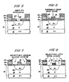
- FIGURES 1-13 A method of fabricating a MOSFET in accordance with a preferred embodiment of our invention will now be described in connection with FIGURES 1-13, illustrating various steps of fabricating a cell (or repeated structure) of a MOSFET.
- a wafer 10 preferably of silicon semiconductor material, comprising an N + substrate 12 having an N layer 14 thereon.
- N layer 14 may typically be epitaxially grown on substrate 12, and is typically on the order of 100 11m thick.
- oxide layer 16 i.e., silicon dioxide
- oxide layer 16 could be used in lieu of oxide layer 16, or oxide layer 16 could instead be formed by other processes, such as by deposition on wafer 10, rather than being thermally grown thereon.
- a top oxide layer 16 we deposit a layer of polysilicon 18 (shown partially removed), or other refractory material, suitably using a process known as Low Pressure Chemical Vapor Deposition (LPCVD).
- LPCVD Low Pressure Chemical Vapor Deposition
- a suitable dopant is the N type dopant phosphorus.
- oxide layer 20 shown partially removed
- Oxide layer 20 should be thicker than oxide layer 16, for a reason that will become apparent below.
- Oxide layer 20 is not essentially needed to practice our invention, however, but we prefer to use it to provide dielectric isolation between the conductive polysilicon layer 18 and source metallization (not yet shown) which will be above the polysilicon layer 18.
- window 22 in oxide layer 20 and polysilicon layer 18, using photolithographic etching techniques.
- the shape of window 22 establishes the shape of the cell of the MOSFET being fabricated; e.g., a round window 22 results in a round cell.
- Such cell can have various shapes, with an elongated, rectangular shape being preferred.
- silicon nitride (Si 3 N 4 ) 24 on the MOSFET cel of FIGURE 2, preferably by LPCVD of a reaction product of silane (SiH 4 ) and ammonia (NH 3 ).
- SiH 4 silane
- NH 3 ammonia
- silicon nitride layer 24 be separated from the upper surface of wafer 10 by oxide layer 16, as illustrated, to avoid mechanical stresses in wafer 10 which tend to develop at a silicon-silicon nitride interface.
- Oxide layer 30 in window 26, preferably by thermal growth resulting from placing wafer 10 in a heated furnace together with an oxidizing ambient.
- Oxide layer 30 must be thicker than oxide layer 16, for a reason that will become apparent below.
- FIGURE 8 we selectively remove exposed portions of oxide layer 16 and portions of both oxide layers 20 and 30.
- This procedure is suitably accomplished by immersing wafer 10 in a solution of hydrofluoric acid (HF) and water (H 2 0) in a ratio of about 1-10 (HF to H 2 0) by volume, for sufficient time to remove the entire exposed portions of oxide layer 16. Less than the entire oxide layers 20 and 30 are removed, however, because they were both originally thicker than oxide layer 16.
- a window 32 is opened, defined by window 22 (FIGURE 2) and oxide layer 30 situated within window 22.
- an oxide layer 40 atop the MOSFET cell of FIGURE 10 preferably by Low Pressure Chemical Vapor Deposition (LPCVD), and then deposit a layer of silicon nitride 42 atop oxide layer 40, preferably by LPCVD of a reaction product of silane (SiH 4 ) and ammonia (NH 3 ).
- LPCVD Low Pressure Chemical Vapor Deposition
- Source metallization 46 to wafer 10, for example, by evaporation of aluminum on the wafer 10.
- Drain metallization 48 may also be applied at this time, to complete the cell of a MOSFET 50, as illustrated in FIGURE 13.
- Oxide layer 40 and silicon nitride 42, together with oxide layer 20, provide dielectric isolation between polysilicon layer 18 and source metallization 46.
- Silicon nitride layer 42 advantageously serves as a sodium barrier between source metallization 46 and wafer 10.
- Layers 20, 40 and 42 could be replaced, however, by one or more different insulating layers, as long as adequate dielectric isolation is provided between polysilicon layer 18 and source metallization 46.
- MOSFET 50 an electrical short in MOSFET 50 is automatically formed across P-N junction 38 by source metallization 46, without requiring that N + source region 38 be etched through to deep P + base region 28, in contrast with the prior art method, described above.
- silicon nitride layer 24 (FIGURE 3 et seq.) has been found to possess three essential properties which make it suitable for use in fabricating a semiconductor device with a base region having a deep portion.
- silicon nitride resists oxidation when placed in a heated furnace together with an oxidizing ambient, as when growing oxide layer 30 (FIGURE 6).
- silicon nitride can be selectively removed without removing silicon dioxide (FIGURE 7).
- silicon nitride serves as a barrier to dopant impurities which are diffused into wafer 10 (FIGURE 5). Materials other than silicon nitride that possess the foregoing properties can be utilized in lieu of silicon nitride layer 24 in carrying out our invention.
- IGR insulated gate rectifier
- FIGURE 14 Another suitable device is an insulated gate rectifier (IGR), illustrated in FIGURE 14.
- IGR. 60 is essentially identical to MOSFET 50 (FIGURE 13) except that in IGR 60 a wafer is provided having an N layer 62 on a P + substrate 64, in contrast with wafer 10 of MOSFET 50 having N type layer 14 on N + type drain substrate region 12. Accordingly, IGR 60 can be fabricated in accordance with the foregoing description of the fabrication of MOSFET 50, taking into account the differences in substrate dopant type.
- IGR 60 Details of the structure and operation of an IGR, such as IGR 60, are described in commonly-assigned U.S. Patent application Serial No. 212,181, filed December 2, 1980, by B. J. Baliga, entitled; "Gate Enhanced Rectifier” (referred to herein as an IGR), and in commonly-assigned U.S. Patent application Serial No. 365,076, filed April 5, 1982, by M. S. Adler and B. J. Baliga, entitled, "Insulated Gate Rectifier With Improved Current-Carrying Capability.”
Landscapes
- Insulated Gate Type Field-Effect Transistor (AREA)
- Bipolar Transistors (AREA)
- Electrodes Of Semiconductors (AREA)
Claims (9)
Applications Claiming Priority (2)
| Application Number | Priority Date | Filing Date | Title |
|---|---|---|---|
| US06/392,870 US4443931A (en) | 1982-06-28 | 1982-06-28 | Method of fabricating a semiconductor device with a base region having a deep portion |
| US392870 | 1982-06-28 |
Publications (3)
| Publication Number | Publication Date |
|---|---|
| EP0097866A2 EP0097866A2 (fr) | 1984-01-11 |
| EP0097866A3 EP0097866A3 (en) | 1986-10-08 |
| EP0097866B1 true EP0097866B1 (fr) | 1990-05-23 |
Family
ID=23552352
Family Applications (1)
| Application Number | Title | Priority Date | Filing Date |
|---|---|---|---|
| EP83105802A Expired - Lifetime EP0097866B1 (fr) | 1982-06-28 | 1983-06-14 | Procédé de fabrication d'un dispositif semi-conducteur à région de base ayant une partie profonde |
Country Status (6)
| Country | Link |
|---|---|
| US (1) | US4443931A (fr) |
| EP (1) | EP0097866B1 (fr) |
| JP (1) | JPS5917283A (fr) |
| DE (1) | DE3381604D1 (fr) |
| IE (1) | IE56041B1 (fr) |
| MX (1) | MX153211A (fr) |
Families Citing this family (56)
| Publication number | Priority date | Publication date | Assignee | Title |
|---|---|---|---|---|
| US4983535A (en) * | 1981-10-15 | 1991-01-08 | Siliconix Incorporated | Vertical DMOS transistor fabrication process |
| US4598461A (en) * | 1982-01-04 | 1986-07-08 | General Electric Company | Methods of making self-aligned power MOSFET with integral source-base short |
| US4809047A (en) * | 1983-09-06 | 1989-02-28 | General Electric Company | Insulated-gate semiconductor device with improved base-to-source electrode short and method of fabricating said short |
| JPS6076144A (ja) * | 1983-10-03 | 1985-04-30 | Matsushita Electronics Corp | 半導体装置の製造方法 |
| DE3402867A1 (de) * | 1984-01-27 | 1985-08-01 | Siemens AG, 1000 Berlin und 8000 München | Halbleiterbauelement mit kontaktloch |
| JPS62501111A (ja) * | 1984-05-02 | 1987-04-30 | インタ−ナショナル・スタンダ−ド・エレクトリック・コ−ポレイション | 半導体装置および配置 |
| IT1214805B (it) * | 1984-08-21 | 1990-01-18 | Ates Componenti Elettron | Spositivi a semiconduttore con giunprocesso per la fabbricazione di dizioni planari a concentrazione di carica variabile e ad altissima tensione di breakdown |
| US4639754A (en) * | 1985-02-25 | 1987-01-27 | Rca Corporation | Vertical MOSFET with diminished bipolar effects |
| GB2173037A (en) * | 1985-03-29 | 1986-10-01 | Philips Electronic Associated | Semiconductor devices employing conductivity modulation |
| EP0202477A3 (fr) * | 1985-04-24 | 1988-04-20 | General Electric Company | Procédé pour former des courts-circuits électriques entre des régions voisines dans un dispositif semi-conducteur à gâchette isolée |
| JPS6252966A (ja) * | 1985-09-02 | 1987-03-07 | Toshiba Corp | 半導体装置の製造方法 |
| DE3689680T2 (de) * | 1985-09-30 | 1994-06-23 | Toshiba Kawasaki Kk | Mittels Steuerelektrode abschaltbarer Thyristor mit unabhängigen Zünd-/Lösch-Kontrolltransistoren. |
| US4809045A (en) * | 1985-09-30 | 1989-02-28 | General Electric Company | Insulated gate device |
| US4963951A (en) * | 1985-11-29 | 1990-10-16 | General Electric Company | Lateral insulated gate bipolar transistors with improved latch-up immunity |
| EP0229362B1 (fr) * | 1986-01-10 | 1993-03-17 | General Electric Company | Dispositif semi-conducteur et méthode de fabrication |
| IT1204243B (it) * | 1986-03-06 | 1989-03-01 | Sgs Microelettronica Spa | Procedimento autoallineato per la fabbricazione di celle dmos di piccole dimensioni e dispositivi mos ottenuti mediante detto procedimento |
| US4816882A (en) * | 1986-03-10 | 1989-03-28 | Siliconix Incorporated | Power MOS transistor with equipotential ring |
| US4798810A (en) * | 1986-03-10 | 1989-01-17 | Siliconix Incorporated | Method for manufacturing a power MOS transistor |
| US5262336A (en) * | 1986-03-21 | 1993-11-16 | Advanced Power Technology, Inc. | IGBT process to produce platinum lifetime control |
| US4716126A (en) * | 1986-06-05 | 1987-12-29 | Siliconix Incorporated | Fabrication of double diffused metal oxide semiconductor transistor |
| FR2605800B1 (fr) * | 1986-10-24 | 1989-01-13 | Thomson Semiconducteurs | Procede de fabrication d'un composant mos |
| JP2552880B2 (ja) * | 1986-11-12 | 1996-11-13 | シリコニックス・インコーポレイテッド | 垂直dmosセル構造 |
| US4883767A (en) * | 1986-12-05 | 1989-11-28 | General Electric Company | Method of fabricating self aligned semiconductor devices |
| JPH0783124B2 (ja) * | 1986-12-05 | 1995-09-06 | ゼネラル・エレクトリック・カンパニイ | セルフアライン半導体装置を製造する方法 |
| US4794432A (en) * | 1987-01-27 | 1988-12-27 | General Electric Company | Mosfet structure with substrate coupled source |
| JPH01225164A (ja) * | 1988-03-03 | 1989-09-08 | Fuji Electric Co Ltd | 絶縁ゲートmosfetの製造方法 |
| US4847671A (en) * | 1987-05-19 | 1989-07-11 | General Electric Company | Monolithically integrated insulated gate semiconductor device |
| US4888627A (en) * | 1987-05-19 | 1989-12-19 | General Electric Company | Monolithically integrated lateral insulated gate semiconductor device |
| US4857983A (en) * | 1987-05-19 | 1989-08-15 | General Electric Company | Monolithically integrated semiconductor device having bidirectional conducting capability and method of fabrication |
| US4795716A (en) * | 1987-06-19 | 1989-01-03 | General Electric Company | Method of making a power IC structure with enhancement and/or CMOS logic |
| JPH0648729B2 (ja) * | 1988-02-24 | 1994-06-22 | シーメンス、アクチエンゲゼルシシヤフト | 電界効果制御可能のバイポーラ・トランジスタ |
| EP0340445B1 (fr) * | 1988-04-22 | 1993-08-25 | Asea Brown Boveri Ag | Dispositif semi-conducteur de puissance, à extinction |
| US4969027A (en) * | 1988-07-18 | 1990-11-06 | General Electric Company | Power bipolar transistor device with integral antisaturation diode |
| US4853345A (en) * | 1988-08-22 | 1989-08-01 | Delco Electronics Corporation | Process for manufacture of a vertical DMOS transistor |
| US5034346A (en) * | 1988-08-25 | 1991-07-23 | Micrel Inc. | Method for forming shorting contact for semiconductor which allows for relaxed alignment tolerance |
| JP2752385B2 (ja) * | 1988-08-29 | 1998-05-18 | ニスコ株式会社 | ドリル型リベット |
| US5072266A (en) | 1988-12-27 | 1991-12-10 | Siliconix Incorporated | Trench DMOS power transistor with field-shaping body profile and three-dimensional geometry |
| US5119162A (en) * | 1989-02-10 | 1992-06-02 | Texas Instruments Incorporated | Integrated power DMOS circuit with protection diode |
| US4931408A (en) * | 1989-10-13 | 1990-06-05 | Siliconix Incorporated | Method of fabricating a short-channel low voltage DMOS transistor |
| IT1236994B (it) * | 1989-12-29 | 1993-05-12 | Sgs Thomson Microelectronics | Processo per la fabbricazione di dispositivi semiconduttori mos di potenza e dispositivi con esso ottenuti |
| US5171705A (en) * | 1991-11-22 | 1992-12-15 | Supertex, Inc. | Self-aligned structure and process for DMOS transistor |
| US5248627A (en) * | 1992-03-20 | 1993-09-28 | Siliconix Incorporated | Threshold adjustment in fabricating vertical dmos devices |
| JP3417013B2 (ja) * | 1993-10-18 | 2003-06-16 | 株式会社デンソー | 絶縁ゲート型バイポーラトランジスタ |
| US5858845A (en) * | 1994-09-27 | 1999-01-12 | Micron Technology, Inc. | Electrically conductive substrate interconnect continuity region and method of forming same with an angled implant |
| US5378641A (en) * | 1993-02-22 | 1995-01-03 | Micron Semiconductor, Inc. | Electrically conductive substrate interconnect continuity region and method of forming same with an angled implant |
| US5395776A (en) * | 1993-05-12 | 1995-03-07 | At&T Corp. | Method of making a rugged DMOS device |
| US5488236A (en) * | 1994-05-26 | 1996-01-30 | North Carolina State University | Latch-up resistant bipolar transistor with trench IGFET and buried collector |
| US5471075A (en) * | 1994-05-26 | 1995-11-28 | North Carolina State University | Dual-channel emitter switched thyristor with trench gate |
| JP3279151B2 (ja) * | 1995-10-23 | 2002-04-30 | トヨタ自動車株式会社 | 半導体装置及びその製造方法 |
| JP3464382B2 (ja) * | 1998-05-18 | 2003-11-10 | ローム株式会社 | 縦型二重拡散mosfetの製造方法 |
| EP0993033A1 (fr) | 1998-10-06 | 2000-04-12 | STMicroelectronics S.r.l. | Structure d'isolation de la grille d' un transistor MOS de puissance et procédé de fabrication |
| DE19958234C2 (de) * | 1999-12-03 | 2001-12-20 | Infineon Technologies Ag | Anordnung eines Gebietes zur elektrischen Isolation erster aktiver Zellen von zweiten aktiven Zellen |
| EP1531497A1 (fr) * | 2003-11-17 | 2005-05-18 | ABB Technology AG | Conception de la cathode d'un IGBT avec une aire de securité ameliorée |
| TWI879736B (zh) * | 2018-07-12 | 2025-04-11 | 日商Flosfia股份有限公司 | 半導體裝置和半導體系統 |
| CN111999632B (zh) * | 2019-05-27 | 2023-02-03 | 合肥晶合集成电路股份有限公司 | Pn结样品的获取方法 |
| CN110176401B (zh) * | 2019-06-13 | 2022-08-30 | 深圳市锐骏半导体股份有限公司 | 一种降低vdmos生产成本的方法 |
Family Cites Families (9)
| Publication number | Priority date | Publication date | Assignee | Title |
|---|---|---|---|---|
| US4181542A (en) * | 1976-10-25 | 1980-01-01 | Nippon Gakki Seizo Kabushiki Kaisha | Method of manufacturing junction field effect transistors |
| JPS5432982A (en) * | 1977-08-18 | 1979-03-10 | Mitsubishi Electric Corp | Manufacture of gate turn off thyristor |
| JPS54161894A (en) * | 1978-06-13 | 1979-12-21 | Toshiba Corp | Manufacture of semiconductor device |
| US4199380A (en) * | 1978-11-13 | 1980-04-22 | Motorola, Inc. | Integrated circuit method |
| FR2460542A1 (fr) * | 1979-06-29 | 1981-01-23 | Thomson Csf | Transistor a effet de champ vertical de puissance pour hautes frequences et procede de realisation d'un tel transistor |
| US4344081A (en) * | 1980-04-14 | 1982-08-10 | Supertex, Inc. | Combined DMOS and a vertical bipolar transistor device and fabrication method therefor |
| US4345265A (en) * | 1980-04-14 | 1982-08-17 | Supertex, Inc. | MOS Power transistor with improved high-voltage capability |
| JPS5726467A (en) * | 1980-07-24 | 1982-02-12 | Fujitsu Ltd | Manufacture of semiconductor device |
| US4593302B1 (en) * | 1980-08-18 | 1998-02-03 | Int Rectifier Corp | Process for manufacture of high power mosfet laterally distributed high carrier density beneath the gate oxide |
-
1982
- 1982-06-28 US US06/392,870 patent/US4443931A/en not_active Expired - Lifetime
-
1983
- 1983-05-24 IE IE1223/83A patent/IE56041B1/en not_active IP Right Cessation
- 1983-06-14 DE DE8383105802T patent/DE3381604D1/de not_active Expired - Lifetime
- 1983-06-14 EP EP83105802A patent/EP0097866B1/fr not_active Expired - Lifetime
- 1983-06-27 MX MX197821A patent/MX153211A/es unknown
- 1983-06-28 JP JP58115291A patent/JPS5917283A/ja active Pending
Also Published As
| Publication number | Publication date |
|---|---|
| EP0097866A2 (fr) | 1984-01-11 |
| EP0097866A3 (en) | 1986-10-08 |
| DE3381604D1 (de) | 1990-06-28 |
| US4443931A (en) | 1984-04-24 |
| MX153211A (es) | 1986-08-22 |
| IE56041B1 (en) | 1991-03-27 |
| IE831223L (en) | 1983-12-28 |
| JPS5917283A (ja) | 1984-01-28 |
Similar Documents
| Publication | Publication Date | Title |
|---|---|---|
| US4443931A (en) | Method of fabricating a semiconductor device with a base region having a deep portion | |
| US5334556A (en) | Method for improving gate oxide integrity using low temperature oxidation during source/drain anneal | |
| EP0094891B1 (fr) | Procédé pour la fabrication d'une structure verticale MOSFET de puissance | |
| US4273805A (en) | Passivating composite for a semiconductor device comprising a silicon nitride (Si1 3N4) layer and phosphosilicate glass (PSG) layer | |
| US3890632A (en) | Stabilized semiconductor devices and method of making same | |
| US4497106A (en) | Semiconductor device and a method of manufacturing the same | |
| EP0034910B1 (fr) | Procédé de fabrication d'un dispositif à semi-conducteur et dispositif ainsi obtenu | |
| US4507171A (en) | Method for contacting a narrow width PN junction region | |
| JP2670563B2 (ja) | 半導体装置の製造方法 | |
| US3943542A (en) | High reliability, low leakage, self-aligned silicon gate FET and method of fabricating same | |
| US4810665A (en) | Semiconductor device and method of fabrication | |
| EP0680093A2 (fr) | Thyristor à induction statique et son procédé de fabrication | |
| EP0076106A2 (fr) | Procédé de fabrication d'un transistor bipolaire | |
| US4668973A (en) | Semiconductor device passivated with phosphosilicate glass over silicon nitride | |
| US3928091A (en) | Method for manufacturing a semiconductor device utilizing selective oxidation | |
| US4054989A (en) | High reliability, low leakage, self-aligned silicon gate FET and method of fabricating same | |
| US4752815A (en) | Method of fabricating a Schottky barrier field effect transistor | |
| US5187108A (en) | Method of manufacturing a bipolar transistor | |
| JPS57134956A (en) | Manufacture of semiconductor integrated circuit | |
| JP2003179066A (ja) | 半導体装置とその製造方法 | |
| JPH0745824A (ja) | 半導体装置 | |
| USRE32351E (en) | Method of manufacturing a passivating composite comprising a silicon nitride (SI1 3N4) layer and a phosphosilicate glass (PSG) layer for a semiconductor device layer | |
| JP2800753B2 (ja) | 接合型電界効果トランジスタの製造方法 | |
| KR0138125B1 (ko) | 트랜지스터의 게이트 유전막 형성 방법 | |
| KR960006433B1 (ko) | 질소원자의 이온주입에 의한 소자분리막 형성 방법 |
Legal Events
| Date | Code | Title | Description |
|---|---|---|---|
| PUAI | Public reference made under article 153(3) epc to a published international application that has entered the european phase |
Free format text: ORIGINAL CODE: 0009012 |
|
| AK | Designated contracting states |
Designated state(s): CH DE FR GB LI NL SE |
|
| 17P | Request for examination filed |
Effective date: 19840329 |
|
| PUAL | Search report despatched |
Free format text: ORIGINAL CODE: 0009013 |
|
| AK | Designated contracting states |
Kind code of ref document: A3 Designated state(s): CH DE FR GB LI NL SE |
|
| 17Q | First examination report despatched |
Effective date: 19890724 |
|
| GRAA | (expected) grant |
Free format text: ORIGINAL CODE: 0009210 |
|
| AK | Designated contracting states |
Kind code of ref document: B1 Designated state(s): CH DE FR GB LI NL SE |
|
| ET | Fr: translation filed | ||
| REF | Corresponds to: |
Ref document number: 3381604 Country of ref document: DE Date of ref document: 19900628 |
|
| PLBE | No opposition filed within time limit |
Free format text: ORIGINAL CODE: 0009261 |
|
| STAA | Information on the status of an ep patent application or granted ep patent |
Free format text: STATUS: NO OPPOSITION FILED WITHIN TIME LIMIT |
|
| 26N | No opposition filed | ||
| EAL | Se: european patent in force in sweden |
Ref document number: 83105802.9 |
|
| PGFP | Annual fee paid to national office [announced via postgrant information from national office to epo] |
Ref country code: GB Payment date: 20010521 Year of fee payment: 19 Ref country code: CH Payment date: 20010521 Year of fee payment: 19 |
|
| PGFP | Annual fee paid to national office [announced via postgrant information from national office to epo] |
Ref country code: DE Payment date: 20010523 Year of fee payment: 19 |
|
| PGFP | Annual fee paid to national office [announced via postgrant information from national office to epo] |
Ref country code: SE Payment date: 20010531 Year of fee payment: 19 |
|
| REG | Reference to a national code |
Ref country code: GB Ref legal event code: IF02 |
|
| PGFP | Annual fee paid to national office [announced via postgrant information from national office to epo] |
Ref country code: FR Payment date: 20020517 Year of fee payment: 20 |
|
| PGFP | Annual fee paid to national office [announced via postgrant information from national office to epo] |
Ref country code: NL Payment date: 20020522 Year of fee payment: 20 |
|
| PG25 | Lapsed in a contracting state [announced via postgrant information from national office to epo] |
Ref country code: GB Free format text: LAPSE BECAUSE OF NON-PAYMENT OF DUE FEES Effective date: 20020614 |
|
| PG25 | Lapsed in a contracting state [announced via postgrant information from national office to epo] |
Ref country code: SE Free format text: LAPSE BECAUSE OF NON-PAYMENT OF DUE FEES Effective date: 20020615 |
|
| PG25 | Lapsed in a contracting state [announced via postgrant information from national office to epo] |
Ref country code: LI Free format text: LAPSE BECAUSE OF NON-PAYMENT OF DUE FEES Effective date: 20020630 Ref country code: CH Free format text: LAPSE BECAUSE OF NON-PAYMENT OF DUE FEES Effective date: 20020630 |
|
| PG25 | Lapsed in a contracting state [announced via postgrant information from national office to epo] |
Ref country code: DE Free format text: LAPSE BECAUSE OF NON-PAYMENT OF DUE FEES Effective date: 20030101 |
|
| EUG | Se: european patent has lapsed | ||
| GBPC | Gb: european patent ceased through non-payment of renewal fee |
Effective date: 20020614 |
|
| REG | Reference to a national code |
Ref country code: CH Ref legal event code: PL |
|
| PG25 | Lapsed in a contracting state [announced via postgrant information from national office to epo] |
Ref country code: NL Free format text: LAPSE BECAUSE OF EXPIRATION OF PROTECTION Effective date: 20030614 |
|
| NLV7 | Nl: ceased due to reaching the maximum lifetime of a patent |
Effective date: 20030614 |