EP0097903A2 - Méthode d'exposition par faisceau d'électrons - Google Patents
Méthode d'exposition par faisceau d'électrons Download PDFInfo
- Publication number
- EP0097903A2 EP0097903A2 EP83106013A EP83106013A EP0097903A2 EP 0097903 A2 EP0097903 A2 EP 0097903A2 EP 83106013 A EP83106013 A EP 83106013A EP 83106013 A EP83106013 A EP 83106013A EP 0097903 A2 EP0097903 A2 EP 0097903A2
- Authority
- EP
- European Patent Office
- Prior art keywords
- electron beam
- resist film
- pattern
- exposure
- exposed
- Prior art date
- Legal status (The legal status is an assumption and is not a legal conclusion. Google has not performed a legal analysis and makes no representation as to the accuracy of the status listed.)
- Granted
Links
Images


Classifications
-
- H—ELECTRICITY
- H10—SEMICONDUCTOR DEVICES; ELECTRIC SOLID-STATE DEVICES NOT OTHERWISE PROVIDED FOR
- H10P—GENERIC PROCESSES OR APPARATUS FOR THE MANUFACTURE OR TREATMENT OF DEVICES COVERED BY CLASS H10
- H10P95/00—Generic processes or apparatus for manufacture or treatments not covered by the other groups of this subclass
-
- B—PERFORMING OPERATIONS; TRANSPORTING
- B82—NANOTECHNOLOGY
- B82Y—SPECIFIC USES OR APPLICATIONS OF NANOSTRUCTURES; MEASUREMENT OR ANALYSIS OF NANOSTRUCTURES; MANUFACTURE OR TREATMENT OF NANOSTRUCTURES
- B82Y10/00—Nanotechnology for information processing, storage or transmission, e.g. quantum computing or single electron logic
-
- B—PERFORMING OPERATIONS; TRANSPORTING
- B82—NANOTECHNOLOGY
- B82Y—SPECIFIC USES OR APPLICATIONS OF NANOSTRUCTURES; MEASUREMENT OR ANALYSIS OF NANOSTRUCTURES; MANUFACTURE OR TREATMENT OF NANOSTRUCTURES
- B82Y40/00—Manufacture or treatment of nanostructures
-
- H—ELECTRICITY
- H01—ELECTRIC ELEMENTS
- H01J—ELECTRIC DISCHARGE TUBES OR DISCHARGE LAMPS
- H01J37/00—Discharge tubes with provision for introducing objects or material to be exposed to the discharge, e.g. for the purpose of examination or processing thereof
- H01J37/30—Electron-beam or ion-beam tubes for localised treatment of objects
- H01J37/317—Electron-beam or ion-beam tubes for localised treatment of objects for changing properties of the objects or for applying thin layers thereon, e.g. for ion implantation
- H01J37/3174—Particle-beam lithography, e.g. electron beam lithography
-
- H—ELECTRICITY
- H01—ELECTRIC ELEMENTS
- H01J—ELECTRIC DISCHARGE TUBES OR DISCHARGE LAMPS
- H01J2237/00—Discharge tubes exposing object to beam, e.g. for analysis treatment, etching, imaging
- H01J2237/30—Electron or ion beam tubes for processing objects
- H01J2237/317—Processing objects on a microscale
- H01J2237/3175—Lithography
- H01J2237/31769—Proximity effect correction
- H01J2237/31771—Proximity effect correction using multiple exposure
Definitions
- This invention relates to an improved method of electron beam exposure.
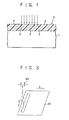
- This electron beam exposure method exposes a positive type (or a negative type) resist film 2 on a mask or a semiconductor substrate 1 as shown in Fig. 1, while scanning it with an electron beam.
- a portion 5 of a marginal area 4 other than a desired exposure area 3 is exposed due to the forward-scattered beams in the resist film 2 and the backward-scattered beams from the substrate 1, causing a problem of what is called "proximity effects", that is, causing the deformation of a pattern configuration.
- One object of this invention is to provide a method of electron beam exposure in which, when a resist film on a substrate is exposed with an electron beam, the scattering of the electron beam in the resist film and the backward beam scattering from the substrate can be suppressed by a simple operation to permit reduction of a proximity effect.
- Another object of this invention is to provide a method of electron beam exposure in which, when a resist film on a substrate is exposed with an electron beam, a difference in a number-average molecular weight between the exposed area and the marginal area in the resist film is increased by a simple operation to permit the reduction of a proximity effect.
- a method of electron beam exposure in which, when a resist film on a substrate is to be selectively exposed with an electron beam, the electron beam is directed onto the resist film a plurality of times in a dose lower than a desired dose sufficient to produce a difference in molecular weight between the exposed area and the nonexposed area, the cumulative dose corresponding to the desired dose.
- the desired dose means a dose determined so that, for the positive type resist film, the number average molecular weight (initial number average molecular weight) of the exposed area is less than two-thirds that of the nonexposed area and that, for the negative type resist film, the number average molecular weight (initial number average molecular weight) of the exposed area is two or more times greater than the nonexposed area.
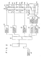
- FIG. 2 is a diagrammatic view showing a raster scan type electron beam exposing apparatus used in this invention.
- An electron gun 11 includes a cathode 12, a .Wehnelt electrode 13 enclosing the cathode 12 and an anode 14 disposed opposite to the Wehnelt electrode 13.
- a first condenser lens 15, second condenser lens 16 and objective lens 17 constituting an electromagnetic lens are vertically arranged, at predetermined distances, below the electron gun 11.
- An alignment coil 181 is disposed between the electron gun 11 and the first condenser lens 15, an alignment coil 18 2 between the first and second condenser lens 15 and 16, and an alignment coil 18 3 between the second condenser lens 16 and the objective lens 17.
- alignment coils 181 - 18 3 are adapted to align an optical axis of electron beams.
- a blanking electrode 19 for effecting ON-OFF control of the electron beam is arranged between the first condenser lens 15 and the alignment coil 182.
- a deflecting plate 20 for scanning the electron beam is disposed between the alignment coil 18 3 and the objective lens 17.
- a stage 21 which is mounted on a base 22 and which is movable in the X, Y directions.
- a reflection electron detector 23 is located above the stage 21.
- a CPU 24 is adapted to control predetermined members of the above-mentioned apparatus, and is connected to an interface 25, which in turn is connected to the electron gun 11 through a bias control circuit 26.
- the control circuit 26 is adapted to control a grid bias between the cathode 12 and the anode 14 of the electron gun 11 to control the flow of the beam.
- the interface 25 is connected to the blanking electrode 19 through a blanking control circuit 27, to the deflecting plate 20 through a deflection control circuit 28, and to the stage 21 through an X-Y stage control circuit 29 and drive system 30.
- a laser length measuring system 31 is arranged with respect to the stage 21 and connected to the interface 25 through a position detector 32.
- a console unit 33 is connected to the CPU 24 to input a dose of the electron beam, beam scanning mode, etc.
- Polymethyl methacrylate was spin-coated on a blank mask 34 and prebaked, followed by coating, for example, a 0.5 pin-thick positive type resist layer on the resultant structure.
- the blank mask 34 was fixed on the stage 21 through a cassette (not shown).
- the CPU 24 operated the bias control circuit 26, blanking control circuit 27, deflection control circuit 28 and X-Y stage control circuit 29 through the interface 25.
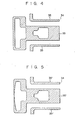
- the blank mask 34 was moved in the Y direction to perform a first exposure in the Y direction as shown in Fig. 3.
- the stage 21 was returned to an original drawing start point and the second exposure was effected on a previously drawn resist film area under the same conditions as mentioned above.
- the stage 21 was stepped in the X direction and exposure was made with the electron beam in the same way. Thereafter, the exposed positive type resist film was subjected to a development step as shown in Fig. 4 to form a resist pattern 35.
- Polymethyl methacrylate was spin-coated on a blank mask and baked, followed by coating a 0.5 ⁇ m-thick resist film of a positive type. Then, the blank mask was fixed on the stage 21 of Fig. 2 through a cassette and an electron beam was directed onto the resist film with an address unit of 0.5 ⁇ m, beam current of 400 nA and exposure time per dot of 50 n sec to perform the first exposure. At this time, the number average molecular weight of the exposed area of the resist film was reduced to one-third the original number average . molecular weight of the nonexposed are of the resist film. Then, the exposed resist film was subjected to a development step to form a resist pattern 35' as shown in Fig. 5.
- the marginal area of the pattern was substantially free from any defective curve which might otherwise be formed due to the proximity effect, thus forming a resist pattern 35 as shown in Fig. 4 which was faithful to the pattern data.
- a resist pattern 35 1 was formed in which a defective curve was formed on the marginal area of the pattern due to the proximity effect.
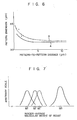
- a plurality of 3 ⁇ m (based on data) patterns were formed according to the methods of Example 1 and Control 1 and a relation of a pattern dimension to a variation in a distance between the patterns was examined to obtain a curve as shown in Fig. 6.
- Fig. 6 A shows the characteristic curve representing a variation of the pattern-dimension as obtained according to the method of Example 1 and B shows the characteristic curve representing a variation of the pattern dimension as obtained according to the method of Control 1.
- the pattern dimension markedly varies if the pattern-to-pattern distance is shorter than 3.0 ⁇ m.
- Example 1 In the method of Example 1, in which the first and second exposures were effected with the electron beam whose dose was one half the desired dose, a variation in the pattern dimension can be suppressed due to a decrease in the proximity effect, even if the pattern-to-pattern distance is shorter than 3.0 ⁇ m. According to the method of Example 1, the proximity effect can be decreased in comparison with that of Control 1, the reason is as follows.
- a lower density exposure area was subjected to the first electron beam exposure to cause the main chains of the area to be initially broken (in the case of a positive type resist film).
- the difference in the number-average molecular weight between the data area and the area affected by the proximity effect was increased in comparison with the difference in the number-average molecular weight between the same areas in the case of Control 1 in which the electron beam exposure was effected once.
- M n denotes the initial number-average molecular weight of the positive type resist film
- Mf is the number-average molecular weight of an area exposed twice with the electron beam whose dose is one half a dose Qo
- Mf is the number-average molecular weight of an area exposed once with a dose of electron beam Qo
- M f ( l ) and Mf( 2 ) are the number-average molecular weights of areas affected due to the proximity effects when the areas are exposed once with a full dose and once with one half the dose of the electron beam Qo.
- the area (Mf(2)) affected due to the proximity effect is less likely to be developed, since the completion of the development step is judged by the exposed area (M f ).
- the area affected due to the proximity effect is less likely to be developed to an extent corresponding to an increase in a difference in the number-average molecular weight between the exposed area and the area affected owing to the proximity effect. It is therefore possible to markedly decrease the proximity effect according to Example 1 as compared with that according to the conventional exposing method.
- a high-sensitivity resist film of a positive type [commercially available under the trade name of EBR-9 (Toray Industries, Inc.)] was spin-coated onto a blank mask and prebaked, followed by coating a 0.6 pm-thick high-sensitivity resist film onto the resultant structure.
- the high-sensitivity resist film was subjected by the electron beam exposure apparatus (Fig. 2) to a first electron beam exposure with an address unit of 0.5 ⁇ m, beam current of 200 nA and exposure time per dot of 25 nsec. Then, the resist film area was again exposed with the electron beam under the same conditions. The exposed resist film was developed to form a resist pattern.
- a 0.6 um-thick high-sensitivity resist film of a positive type was coated onto a blank mask in the same way as in Example 2. Then, an electron beam was directed once onto the high-sensitivity resist film with an address unit of 0.5 pm, a beam current of 400 nA and an exposure time per dot of 25 n sec, while using the electron beam exposure apparatus of Fig. 2. Then, the exposed high-sensitivity resist film of a positive type was developed to form a resist pattern.
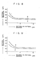
- a plurality of 3 ⁇ m (based on data) patterns were formed according to the method of Example 2 and the method of control 2.
- a relation of a variation of the pattern dimension to a variation in a pattern-to-pattern distance was examined to obtain a curve as shown in Fig. 8.
- a plurality of 2 ⁇ m (based on data) patterns were formed according to the methods of Example 2 and Control 2 and a relation of a variation of the pattern dimension to a distance between the patterns was examined to obtain a curve as shown in Fig. 9.
- A illustrates a characteristic curve showing a variation of the pattern dimension according to the method of Example 2
- B illustrates a characteristic curve showing a variation of the pattern dimension according to the method of Control 2.
- a plurality of 1 ⁇ m (based on data) patterns were formed according to the methods of Example 2 and Control 2 and a relation of a variation of the pattern dimension to a variation in a pattern-to-pattern distance was examined to obtain a curve as shown in Fig. 10.
- Fig. 10 A illustrates a characteristic curve showing a variation in the pattern dimension according to the method of Example 2 and B illustrates a characteristic curve showing a variation in the pattern dimension according to the method of Control 2.
- a 0.5 ⁇ m-thick resist film of a positive type made of polymethyl methacrylate was coated on a blank mask according to the same method as in Example 1.
- An electron beam was directed once, by the electron beam exposure apparatus (Fig. 2), onto the resist film with an address unit of 0.5 ⁇ m, beam current of 200 nA and exposure time per dot of 50 n sec. Then, the electron beam was again directed onto the once-exposed resist film area under the same conditions.
- the exposed resist film was subjected to a development step to form a resist pattern.
- Example 3 A plurality of 3 ⁇ m (based on data) patterns were formed according to the method of Example 3. A relation of a variation of the pattern dimension to the pattern-to-pattern distance was examined, obtaining a curve as shown in Fig. 11.
- the variation of the pattern dimension can be suppressed, as shown in Fig. 11, owing to a decrease of the proximity effect, as in Example 1 in which the electron beam was twice directed to the resist film during an exposure time per dot which was one half the desired exposure time per dot.
- a 0.5 p m-thick resist film of a positive film made of polymethyl methacrylate was coated on a blank mask using the same method as in Example 1. Then, an electron beam was directed, by the electron beam exposure apparatus (Fig. 2), onto a resist film with an address unit of 0.5 ⁇ m, a beam current of 100 nA and an exposure time per dot of 50 n sec. Then, the exposed resist area was exposed three times (four times in total) with the electron beam under the same conditions. The exposed resist film was subjected to a development step to form a resist pattern.
- Example 4 A plurality of 3 ⁇ m (based on data) patterns were formed by the method of Example 4 and a relation of the variation of a pattern dimension to the variation of a pattern-to-pattern distance was examined to obtain a curve as shown in Fig. 12.
- the variation of the pattern dimension can be further suppressed due to a decrease in the proximity effect, as compared with that of Example 3.
- a 0.5 ⁇ m-thick resist film of a positive type made of polymethyl methacrylate was coated on a blank mask in the same method as in Example 1.
- An electron beam was directed onto the resist film twice by the electron beam exposure apparatus (Fig. 2), with an address unit of 0.5 um, a beam current of 200 nA and an exposure time per dot of 50 n sec. Then, the exposed resist film was developed to form 2 ⁇ m (based on the data) patterns at intervals of 2 ⁇ m.
- the electron beam was directed four times by the electron beam exposure apparatus (Fig. 2) onto the positive type resist film with an address unit of 0.5 ⁇ m, beam current of 100 nA and exposure time per dot of 50 n sec. After this exposure, the resist film was developed to obtain 2 ⁇ m (based on data) patterns at intervals of 2 ⁇ m (based on data).
- the dimensional variation (AL) of the resist patterns formed by the twice-and four-times-exposure methods were examined to obtain a curve as shown in Fig. 13.
- the dimensional variation (AL) was found by subtracting the data value from a dimensional value of measurement of the resist patterns.
- the first exposure was made with an address unit of 0.5 ⁇ m, electron beam current of 400 nA.and exposure time per dot of 50 n sec, and the exposed resist film was subjected to a development step, forming a 2 ⁇ m (based on data) patterns at intervals of 2 ⁇ m (based on data). From Fig. 13 it may be seen that, with respect to the dimensional variation resulting from the proximity effect, the single-exposure method results in a larger variation than does the double-exposure method, and a much larger smaller variation than the four- exposure method.
- the blank mask was used as the substrate
- a semiconductor wafer such as a silicon wafer may be used instead.
- the same result can be obtained even if a negative type resist film is used in place of the positive type resist film.
- this invention provides a method of electron beam exposure, in which a very fine, accurate pattern substantially free from any proximity effect can be obtained by a simple operation, i.e., without using any complicated means such as correction of the pattern data.
Landscapes
- Engineering & Computer Science (AREA)
- Chemical & Material Sciences (AREA)
- Nanotechnology (AREA)
- Crystallography & Structural Chemistry (AREA)
- Physics & Mathematics (AREA)
- Theoretical Computer Science (AREA)
- Mathematical Physics (AREA)
- Condensed Matter Physics & Semiconductors (AREA)
- General Physics & Mathematics (AREA)
- Manufacturing & Machinery (AREA)
- Analytical Chemistry (AREA)
- Electron Beam Exposure (AREA)
- Exposure And Positioning Against Photoresist Photosensitive Materials (AREA)
Applications Claiming Priority (2)
| Application Number | Priority Date | Filing Date | Title |
|---|---|---|---|
| JP112986/82 | 1982-06-30 | ||
| JP57112986A JPS594017A (ja) | 1982-06-30 | 1982-06-30 | 電子ビ−ム露光方法 |
Publications (3)
| Publication Number | Publication Date |
|---|---|
| EP0097903A2 true EP0097903A2 (fr) | 1984-01-11 |
| EP0097903A3 EP0097903A3 (en) | 1985-10-23 |
| EP0097903B1 EP0097903B1 (fr) | 1989-12-27 |
Family
ID=14600546
Family Applications (1)
| Application Number | Title | Priority Date | Filing Date |
|---|---|---|---|
| EP83106013A Expired EP0097903B1 (fr) | 1982-06-30 | 1983-06-20 | Méthode d'exposition par faisceau d'électrons |
Country Status (4)
| Country | Link |
|---|---|
| US (1) | US4644170A (fr) |
| EP (1) | EP0097903B1 (fr) |
| JP (1) | JPS594017A (fr) |
| DE (1) | DE3381033D1 (fr) |
Cited By (1)
| Publication number | Priority date | Publication date | Assignee | Title |
|---|---|---|---|---|
| US4712013A (en) * | 1984-09-29 | 1987-12-08 | Kabushiki Kaisha Toshiba | Method of forming a fine pattern with a charged particle beam |
Families Citing this family (10)
| Publication number | Priority date | Publication date | Assignee | Title |
|---|---|---|---|---|
| JPS6229135A (ja) * | 1985-07-29 | 1987-02-07 | Advantest Corp | 荷電粒子ビ−ム露光方法及びこの方法を用いた荷電粒子ビ−ム露光装置 |
| JPH0645021Y2 (ja) * | 1989-03-10 | 1994-11-16 | サンウエーブ工業株式会社 | ヒンジ装置 |
| US5051598A (en) * | 1990-09-12 | 1991-09-24 | International Business Machines Corporation | Method for correcting proximity effects in electron beam lithography |
| US6534242B2 (en) | 1997-11-06 | 2003-03-18 | Canon Kabushiki Kaisha | Multiple exposure device formation |
| US6377337B1 (en) | 1998-05-02 | 2002-04-23 | Canon Kabushiki Kaisha | Projection exposure apparatus |
| JP3352405B2 (ja) | 1998-09-10 | 2002-12-03 | キヤノン株式会社 | 露光方法及びそれを用いたデバイス製造方法並びに半導体デバイス |
| JP2001126980A (ja) * | 1999-11-01 | 2001-05-11 | Nikon Corp | 蓄積エネルギー計算方法、プログラム記憶媒体、近接効果計算方法、マスク又はレチクルパターンの設計方法、及び半導体デバイスの製造方法 |
| JP2003142500A (ja) * | 2001-10-30 | 2003-05-16 | Fujitsu Ltd | 半導体装置の製造方法 |
| JP4291037B2 (ja) | 2003-05-07 | 2009-07-08 | スガツネ工業株式会社 | スライドヒンジ |
| US8539392B2 (en) | 2011-02-24 | 2013-09-17 | National Taiwan University | Method for compensating proximity effects of particle beam lithography processes |
Family Cites Families (7)
| Publication number | Priority date | Publication date | Assignee | Title |
|---|---|---|---|---|
| DE2143737A1 (de) * | 1971-09-01 | 1973-03-08 | Ibm Deutschland | Photoaetzverfahren |
| JPS51147262A (en) * | 1975-06-13 | 1976-12-17 | Fujitsu Ltd | Electronic beam exposure method |
| US4099062A (en) * | 1976-12-27 | 1978-07-04 | International Business Machines Corporation | Electron beam lithography process |
| DE2852961A1 (de) * | 1978-12-07 | 1980-06-19 | Siemens Ag | Verfahren zum aufbringen sehr feiner strukturen auf ein substrat |
| JPS5596942A (en) * | 1979-01-19 | 1980-07-23 | Matsushita Electric Ind Co Ltd | Method and apparatus for producing minute pattern |
| DE2927242A1 (de) * | 1979-07-05 | 1981-01-08 | Siemens Ag | Korpuskel- oder roentgenlithografisches verfahren zur strukturerzeugung |
| JPS56112729A (en) * | 1980-02-08 | 1981-09-05 | Fujitsu Ltd | Exposure of electron beam |
-
1982
- 1982-06-30 JP JP57112986A patent/JPS594017A/ja active Pending
-
1983
- 1983-06-20 EP EP83106013A patent/EP0097903B1/fr not_active Expired
- 1983-06-20 DE DE8383106013T patent/DE3381033D1/de not_active Expired - Lifetime
-
1985
- 1985-12-20 US US06/810,848 patent/US4644170A/en not_active Expired - Lifetime
Cited By (1)
| Publication number | Priority date | Publication date | Assignee | Title |
|---|---|---|---|---|
| US4712013A (en) * | 1984-09-29 | 1987-12-08 | Kabushiki Kaisha Toshiba | Method of forming a fine pattern with a charged particle beam |
Also Published As
| Publication number | Publication date |
|---|---|
| EP0097903A3 (en) | 1985-10-23 |
| JPS594017A (ja) | 1984-01-10 |
| US4644170A (en) | 1987-02-17 |
| DE3381033D1 (de) | 1990-02-01 |
| EP0097903B1 (fr) | 1989-12-27 |
Similar Documents
| Publication | Publication Date | Title |
|---|---|---|
| US6249597B1 (en) | Method of correcting mask pattern and mask, method of exposure, apparatus thereof, and photomask and semiconductor device using the same | |
| US6147355A (en) | Pattern forming method | |
| EP0206633B1 (fr) | Méthode et appareil pour l'inspection de masques | |
| EP0334680B1 (fr) | Système de réparation des masques | |
| US6835942B2 (en) | Method for correcting a proximity effect, an exposure method, a manufacturing method of a semiconductor device and a proximity correction module | |
| JP2003243291A (ja) | 露光条件監視方法およびその装置並びに半導体デバイスの製造方法 | |
| EP0097903A2 (fr) | Méthode d'exposition par faisceau d'électrons | |
| EP0367126B1 (fr) | Méthode d'exposition au rayonnement de particules chargées utilisant un masque | |
| EP0078579B1 (fr) | Méthode d'utilisation d'un faisceau d'électrons | |
| US20020127881A1 (en) | Step mask | |
| KR19980024385A (ko) | 전자빔 기록 장치와 그곳에 사용되는 제2구멍부재 및 가변 성형 빔 크기의 조정 방법 | |
| JP3105580B2 (ja) | 荷電粒子線描画用マスク作成方法及びマスク | |
| US4788117A (en) | Semiconductor device fabrication including a non-destructive method for examining lithographically defined features | |
| US6182369B1 (en) | Pattern forming apparatus | |
| KR100256519B1 (ko) | 전자빔 노광 보정 방법 | |
| JPS6258621A (ja) | 微細パタ−ン形成方法 | |
| US5516605A (en) | Photo mask provided with development rate measuring pattern and method for measuring development rate uniformity | |
| EP0078578B1 (fr) | Méthode d'utilisation d'un faisceau d'électrons | |
| US6928184B2 (en) | Instrument and method for metrology | |
| KR100688483B1 (ko) | 웨이퍼 또는 상기 웨이퍼 상의 물질층을 건식식각시발생하는 로딩효과로 인한 선폭변화를 보정하는 방법 | |
| McCord et al. | Effect of mask absorber thickness on x‐ray exposure latitude and resolution | |
| Flack et al. | Characterization of mask fabrication for submicron geometries using a shaped vector electron-beam system | |
| US6204511B1 (en) | Electron beam image picturing method and image picturing device | |
| JP2001237175A (ja) | 近接効果補正方法、レチクル及びデバイス製造方法 | |
| Studebaker et al. | Prototype to production using the Hewlett–Packard quarter‐micron electron beam system |
Legal Events
| Date | Code | Title | Description |
|---|---|---|---|
| PUAI | Public reference made under article 153(3) epc to a published international application that has entered the european phase |
Free format text: ORIGINAL CODE: 0009012 |
|
| 17P | Request for examination filed |
Effective date: 19830715 |
|
| AK | Designated contracting states |
Designated state(s): DE FR GB |
|
| RAP1 | Party data changed (applicant data changed or rights of an application transferred) |
Owner name: KABUSHIKI KAISHA TOSHIBA |
|
| PUAL | Search report despatched |
Free format text: ORIGINAL CODE: 0009013 |
|
| AK | Designated contracting states |
Designated state(s): DE FR GB |
|
| 17Q | First examination report despatched |
Effective date: 19870318 |
|
| GRAA | (expected) grant |
Free format text: ORIGINAL CODE: 0009210 |
|
| AK | Designated contracting states |
Kind code of ref document: B1 Designated state(s): DE FR GB |
|
| REF | Corresponds to: |
Ref document number: 3381033 Country of ref document: DE Date of ref document: 19900201 |
|
| ET | Fr: translation filed | ||
| PLBE | No opposition filed within time limit |
Free format text: ORIGINAL CODE: 0009261 |
|
| STAA | Information on the status of an ep patent application or granted ep patent |
Free format text: STATUS: NO OPPOSITION FILED WITHIN TIME LIMIT |
|
| 26N | No opposition filed | ||
| PGFP | Annual fee paid to national office [announced via postgrant information from national office to epo] |
Ref country code: FR Payment date: 19970610 Year of fee payment: 15 |
|
| PGFP | Annual fee paid to national office [announced via postgrant information from national office to epo] |
Ref country code: GB Payment date: 19970611 Year of fee payment: 15 |
|
| PGFP | Annual fee paid to national office [announced via postgrant information from national office to epo] |
Ref country code: DE Payment date: 19970630 Year of fee payment: 15 |
|
| PG25 | Lapsed in a contracting state [announced via postgrant information from national office to epo] |
Ref country code: GB Free format text: LAPSE BECAUSE OF NON-PAYMENT OF DUE FEES Effective date: 19980620 |
|
| GBPC | Gb: european patent ceased through non-payment of renewal fee |
Effective date: 19980620 |
|
| PG25 | Lapsed in a contracting state [announced via postgrant information from national office to epo] |
Ref country code: FR Free format text: LAPSE BECAUSE OF NON-PAYMENT OF DUE FEES Effective date: 19990226 |
|
| PG25 | Lapsed in a contracting state [announced via postgrant information from national office to epo] |
Ref country code: DE Free format text: LAPSE BECAUSE OF NON-PAYMENT OF DUE FEES Effective date: 19990401 |
|
| REG | Reference to a national code |
Ref country code: FR Ref legal event code: ST |