EP0098153A2 - Circuit de conversion de données numériques pour un code de données à longueur de mot variable - Google Patents
Circuit de conversion de données numériques pour un code de données à longueur de mot variable Download PDFInfo
- Publication number
- EP0098153A2 EP0098153A2 EP83303732A EP83303732A EP0098153A2 EP 0098153 A2 EP0098153 A2 EP 0098153A2 EP 83303732 A EP83303732 A EP 83303732A EP 83303732 A EP83303732 A EP 83303732A EP 0098153 A2 EP0098153 A2 EP 0098153A2
- Authority
- EP
- European Patent Office
- Prior art keywords
- word
- data
- circuit
- length
- variable
- Prior art date
- Legal status (The legal status is an assumption and is not a legal conclusion. Google has not performed a legal analysis and makes no representation as to the accuracy of the status listed.)
- Granted
Links
Images


Classifications
-
- G—PHYSICS
- G11—INFORMATION STORAGE
- G11B—INFORMATION STORAGE BASED ON RELATIVE MOVEMENT BETWEEN RECORD CARRIER AND TRANSDUCER
- G11B20/00—Signal processing not specific to the method of recording or reproducing; Circuits therefor
- G11B20/10—Digital recording or reproducing
- G11B20/14—Digital recording or reproducing using self-clocking codes
- G11B20/1403—Digital recording or reproducing using self-clocking codes characterised by the use of two levels
- G11B20/1423—Code representation depending on subsequent bits, e.g. delay modulation, double density code, Miller code
- G11B20/1426—Code representation depending on subsequent bits, e.g. delay modulation, double density code, Miller code conversion to or from block codes or representations thereof
-
- G—PHYSICS
- G11—INFORMATION STORAGE
- G11B—INFORMATION STORAGE BASED ON RELATIVE MOVEMENT BETWEEN RECORD CARRIER AND TRANSDUCER
- G11B20/00—Signal processing not specific to the method of recording or reproducing; Circuits therefor
- G11B20/10—Digital recording or reproducing
- G11B20/10527—Audio or video recording; Data buffering arrangements
-
- H—ELECTRICITY
- H03—ELECTRONIC CIRCUITRY
- H03M—CODING; DECODING; CODE CONVERSION IN GENERAL
- H03M7/00—Conversion of a code where information is represented by a given sequence or number of digits to a code where the same, similar or subset of information is represented by a different sequence or number of digits
- H03M7/30—Compression; Expansion; Suppression of unnecessary data, e.g. redundancy reduction
- H03M7/40—Conversion to or from variable length codes, e.g. Shannon-Fano code, Huffman code, Morse code
- H03M7/42—Conversion to or from variable length codes, e.g. Shannon-Fano code, Huffman code, Morse code using table look-up for the coding or decoding process, e.g. using read-only memory
Definitions
- the present invention relates to a digital data code conversion circuit for a variable-word-length data code. More particularly, the present invention relates to a digital data code conversion circuit for a variable--word-length data code wherein a preparation circuit is provided for dividing an input variable-word-length data code supplied in parallel into data codes having word lengths less than or equal to a predetermined length.
- variable-word-length data coding system wherein the bit number contained in one word is varied in accordance with the content of information
- the other type is a fixed-word-length data coding system wherein the bit number contained in one word is always constant.
- the variable-word-length data coding system has the advantage that the total number of bits required for the same information is small when compared with the fixed-word-length data coding system. Accordingly, the variable-word-length data coding system is widely used in the transmission of video signals, and voice signals. However, in the variable-word-length data coding system, the bit number contained in a word differs.
- variable-word-length data coding system can be eliminated by dividing and combining a series of data codes having different lengths so as to convert them into a series of parallel data codes having a constant length. To accomplish this, a conversion circuit for converting a variable-word-length data code into a fixed-word-length data code is required.
- a prior art digital data code conversion circuit for a variable-word-length data code is disclosed in Japanese Patent Application JP-A-55-017,259.
- code pattern information for a variable-word-length data code having a word length of up to n bits is input in parallel through data input terminals, and word-length information representing the bit number of the input variable-word-length data code is input through word length input terminals.
- the input variable-word-length data code is converted in the conversion circuit, and a fixed-word-length data code with n-bits is output.
- a digital data conversion circuit comprises a data code conversion portion for converting variable-word-length data codes having a word-length less than or equal to a predetermined number n into fixed-word-length data codes having a word-length equal to the predetermined number n by dividing and combining the input variable-word-length data codes according to word-length information for said input variable-word-length data codes; and a preparation circuit arranged in a stage preceding the data code conversion portion, the preparation circuit dividing an input variable word length data code having a word-length greater than the predetermined number n into a plurality of variable word length data codes each having a word-length less than or equal to the predetermined number n and producing word-length information for the plurality of variable-word-length data codes, wherein the data code conversion portion is operated at an operation rate proportional to the data input rate multiplied by the number of divisions of the variable-word-length data codes.
- a data code having a word length larger than that of output fixed-word-length data can be processed.
- This enables input data codes having a large maximum word length can be processed by a -device having a relatively small circuit scale. This enables the constructions of a control circuit and the control operation to be simplified.
- FIG. lA A system for encoding a variable-word-length data code is illustrated in Fig. lA, and a system for decoding a variable-word-length data code is illustrated in Fig. 1B.
- the system of Fig. 1A comprises a pulse-coded modulator 11, a subtractor 12, a quantizing circuit 13, an adder 14, a prediction circuit 15, a digital-to--digital converter 16, a digital data code conversion circuit 17, and a buffer memory 18.
- an input data signal such as a video signal or a voice signal
- a parallel 8-bit pulse-code modulation (PCM) data code is output from the pulse-coded modulator 11.
- the PCM data code is supplied to the subtractor: 12, is subtracted by a predicting value from the prediction circuit 15, and is then supplied to the quantizing circuit 13.
- the supplied data code is quantized at several quantum levels, for example, 8 levels or 16 levels, and one quantum level signal is output from the quantizing circuit 13.
- the quantum level signal is supplied to the adder 14 and to the digital-to-digital converter 16.
- the quantum level signal is added to the forgoing predicting value and is supplied to the prediction circuit 15 as the next predicting value.
- the digital--to-digital converter 16 the quantum level signal is converted into a variable-word-length data code.
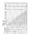
- variable-word-length data codes is illustrated in Fig. 2.
- the input data is quantized in 16 quantum levels, and each of these quantum levels corresponds to one data pattern of 4 bits as shown in Fig. 2.
- These quantum levels i.e., data patterns
- the word length of each variable-word-length data code is assigned so that the data code corresponding to the quantum level having a smaller absolute value has a shorter word length. Since the quantum level signals output from the quantizing circuit 13 represent the difference between the actual signal data and its predicting value, most of the samples of the output quantum level signals have small absolute values.
- the average word length of the variable-word-length data codes being output from the,digital-to-digital converter 16 becomes very small, for example, 2 or 3 bits. Accordingly, the total data length of information to be transmitted becomes shorter in the variable-word-length data codes than in the PCM data codes.
- variable-word-length data codes output from the digital-to-digital converter 16 are supplied to the digital data code conversion circuit 17 and are converted into fixed-word-length data codes.
- the operation of the digital data code conversion circuit 17 will be described in detail later.
- the fixed-word-length data codes from the conversion circuit 17 are supplied to the buffer memory 18 and are stored therein.
- the stored data codes are transmitted by a transmitting circuit (not shown).
- the system for decoding the variable-word-length data code of Fig. 1B comprises a buffer memory 21, a digital data code conversion circuit 22, a digital-to--digital converter 23, an adder 24, and an integrating circuit 25.
- the received data codes transmitted from the system of Fig. lA are stored in the buffer memory 21.
- the stored data codes are supplied to the digital data code conversion circuit 22 and are converted conversely into variable-word-length data codes as shown in Fig. 2.
- the variable-word-length data codes from the conversion circuit 22 are supplied to the digital-to-digital converter 23 and are converted conversely into quantum level signals.
- the quantum level signals for the converter 23 are supplied to the adder 24 and are added to the output date codes from the integrating circuit 25.
- the output data codes from the adder 24 are output as reproduced PCM data codes.
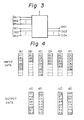
- FIG. 3 A prior art digital data code conversion circuit for a variable-word-length data code which may be used in the system of Fig. 1A is illustrated in Fig. 3.
- the digital data code conversion circuit 1 of Fig. 3 has n-bit code pattern information input terminals DI1, DI2, ---, DIn, m-bit word-length ,information input terminals BN1, BN2, ---, DNm, and n-bit output terminals D01, D02, ---, DOn.
- variable-length data codes being input from the code pattern information input terminals DI1, DI2, ---, DIn are converted into fixed-word-length data codes, and the converted n-bit fixed-word-length data codes are output from the output terminals DOl, D02, ---, DOn.
- FIG. 4 The operation of the digital data code conversion circuit 1 of Fig. 3 is described with reference to the input and output data example of Fig. 4.
- input data series (A), (B), ---, (F) are input into the digital data code conversion circuit 1 in sequence. Since the first input data (A) is 6-bit data, the leading 2 bits of the next input data (B) are attached to the end of the input data (A), and the 8-bit output data (A') is output. Then, since the last 1 bit of the input data (B) remains, the leading 7 bits of the next input data (C) are attached to the remaining 1 bit, and the 8-bit output data (B') is output.
- the above-mentioned conversion operation may be carried out by the circuit disclosed in the foregoing Japanese Patent Application JP-A-55-017,259.
- the word length of an input variable-word-length data code must be less than or equal to the predetermined number n.
- an input data code having a word length greater than the number n cannot be processed by the data code conversion circuit.
- the variable--word-length data codes shown in Fig. 2 which codes may have 16 bits at the maximum, cannot be processed by the above-mentioned 8-bit data code conversion circuit.
- a digital data code conversion circuit for a variable-word-length data code according to the present invention is illustrated in Fig. 5.
- the digital data code conversion circuit of Fig. 5 comprises a preparation circuit 3 and a data code conversion portion 4.
- the preparation circuit 3 has variable-word-length data pattern input terminals DIl, DI2, ---, DIn 0 ' word-length input terminals BNl, BN2, ---, BNm 0 , variable-word--length data pattern output terminals DI'l, DI'2, ---, DI'n 1 , and word-length output terminals BN'l, BN'2, ---, BN'm 1 .
- the 8-bit data code and the 7-bit data code are supplied in sequence to the data code conversion portion 4 along with the pieces of word-length information representing 8 bits and 7 bits. These two data codes are processed in the data code conversion portion 4 in the same manner as in the conversion circuit 1 of Fig. 3.
- the preparation circuit 3 of Fig. 6 comprises a flip-flop circuit 31 for receiving the word-length information input, a flip-flop circuit 32 for receiving the data code information input, a word-length information conversion circuit 33 for converting the input word-length information into word-length information for the divided data codes, a data code selector circuit 34 for selecting one data code from the divided data codes, a word-length selector circuit 35 for selecting one piece of word-length information from the pieces of information for the divided data codes, a flip-flop circuit 36 for outputting the word-length information for the divided data code, a flip-flop circuit 37 for outputting the divided data code, and a control circuit 38 for controlling the above-mentioned circuits 3l through 37.
- Word-length information representing 15 bits and the 15-bit data code are written into the flip-flop circuits 31 and 32, respectively, by the clock signal CLK.
- the word-length information written into the flip-flop circuit 31 is supplied to the word-length information conversion circuit 33 and is converted into two pieces of word-length information representing 8 bits and 7 bits.
- the data code written into the flip-flop circuit 32 is supplied to the data code selector circuit 34 and is divided into two data codes, one of which consists of the most significant 8 bits and the other of which consists of the least significant 7 bits.
- the data code consisting of the most significant 8 bits is output first, and the data code consisting of the least significant 7 bits is output next by being selected according to the select signal from the control circuit 38.
- the word-length imformation representing 8 bits is selected and is output first from the selector circuit 35.
- the word-length information representing 7 bits is selected and is output.
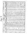
- a word length of up to 16 bits can be represented by a 5-bit signal, and a word length of up to 8 bits can be represented by a 4-bit signal.
- the data patterns of the input word-length information and the corresponding output word-length information are illustrated in Fig. 7. As can be seen from Fig. 7, if the word length of the input data code is less than or equal to 8 bits, the word length of the first output data code is equal to that of the input data code, and the word length of the second output data code is zero bit. If the word length of the input data code is from 9 to 16 bits, the word length of the first output data code is 8 bits, and the word length of the second output data code is equal to a number less than that of the input data code by 8.
- the word-length information conversion circuit 33 and the word-length selector circuis 35 may be constructed as shown in Fig. 8.
- the word--length information B 1 , B 2 , ---, B : of the input data code is converted into the word-length information Cl , C2 , ---, C4 of the first output data code and the word-length information Dl , D2 , ---, D4 of the second output data code.
- an input variable-word-length data code of up to 16 bits is divided into two output variable-word-length data codes of up to 8 bits.
- These output variable-word--length data.codes are supplied in sequence to the data code conversion portion 4 and are converted into 8-bit data codes.
- an input variable-word--length data code of up to 16 bits can be processed by an 8-bit data code conversion portion.
- an input variable-word-length data code greater than 16 bits can be processed by the conversion circuit of Fig. 6.
- the data code conversion portion 4 of Fig. 9 comprises a matrix-type rotation circuit 41 for receiving a variable-word-length data code of up to n 1 bits, a first register circuit 42 for receiving the n 1 bit output signal from the rotation circuit 41, a first selector circuit 43, a second selector circuit 44, a second register circuit 45, a third register circuit 46, and a control circuit 47 for controlling the above-mentioned circuits 41 through 46.
- the first selector circuit 43 receives an output data signal from the first register'circuit 42 and an output data signal from the second register circuit 45.
- the second selector circuit 44 receives an output data signal from the rotation circuit 41 and an output data signal from the first selector circuit 43.
- the second register circuit 45 receives an output data signal from the second selector circuit 44.
- the third register circuit 46 receives an output data signal from the second register circuit 45 and outputs the converted fixed-word-length data code.
- the control circuit 47 receives word-length information signal BN'l through BN'm 1 and a clock signal CLK'.
- the operation of the data code conversion portion 4 of Fig. 9 is described with reference to an example of the input data codes shown in Fig. 10. Assume that the data code conversion portion 4 has an 8-bit construction and that the variable-word-length data codes (A) through' (F) shown in Fig. 10 are input into the conversion portion 4 of Fig. 9 in sequence.
- the input data signal Sl is rotated by the bit number determined by the control signal from the control circuit 47 in the rotation circuit 41, and the rotated data signal S2 output from the rotation circuit 41 is supplied to the first register circuit 42 and to the second selector circuit 44.
- the first input data (A) is output from the rotation circuit 41 without being rotated.
- the data (A) is selected and is output by the second selector circuit 44 as the signal S3 and is written into the second register circuit 45.
- the second register circuit 45 since only 6 bits as effective data are written into the second register circuit 45, it is necessary to attach the leading 2 bits of the next input data (B) to the end of the effective 6 bits.
- the second input data (B) is rotated in the rotation circuit 41 so as to arrange the leading 2 bits of the data (B) at the end of the 8-bit data.
- This rotated data is supplied to the first register circuit 42 and to the second selector circuit 44.
- the output data S4 from the second register circuit 45 is selected by the first selector circuit 43 and is supplied to the second selector circuit 44.
- the data from the first selector circuit 43 is selected with regard to the leading 6 bits and the data from the rotation circuit 41 is selected with regard to the remaining 2 bits, and 8-bit data combined as shown in Fig. 10 is output from the second selector circuit 44 (as S3).
- This data S3 is written into the second register circuit 45.
- the data S2 from the rotation circuit 41 is written into the first register circuit 42. Since 8-bit effective data is written into the second register circuit 45, the output data S4 from the second register circuit 45 is written into the third register circuit 46 by the clock signal from the control circuit 47 and is output from the third register circuit 46 as the first output data (A').
- the third input data (C) is rotated by 1 bit in the rotation circuit 41 so as to be attached to the remaining 1 bit of the preceding input data (B), and the rotated data is supplied to the first register circuit 42 and to the second selector circuit 44.
- the data output from the first register circuit 42 is selected by the first selector circuit 43 and is supplied to the second selector circuit 44.
- the data from the first selector circuit 43 is selected with regard to the leading 1 bit
- the data Sl from the rotation circuit 41 is selected with regard to the remaining 7 bits.
- the combined data S3 output from the second selector circuit 44 is supplied to the second register circuit 45 and is written into the second register circuit 45. Since effective 8 bits are written into the second register circuit 45, the output data S4 from the second register circuit 45 is written into the third register circuit 46 and is output from the third register circuit 46 as the second output data (B').
- the above-mentioned operation of the data code conversion portion 4 can be carried out under the control of the control circuit 47.
- the control circuit 47 may be constructed as shown in Fig. 9.
- the control circuit 47 of Fig. 9 comprises an adder circuit 471, a bit number register 472, digital-to-digital converter circuits 473 and 474, an inverter circuit 475, and an AND gate circuit 476.
- the word-length information BN1 through BNm is supplied to the adder circuit 471 and is added to the output of the bit number register 472.
- the output of the adder circuit 471 is supplied to the bit number register 472 and is written into the bit number register 472.
- the bit number register 472 outputs bit number data indicating the number of effective bits written into the second register circuit 45 and a "full" signal indicating that 8 effective bits have been written into the second register circuit 45.
- Bit number data from the bit number register 472 is supplied to the digital-to-digital converter circuits 473 and 474.
- the bit number data is converted into control signals for the rotation circuit 41 and for the second selector circuit 44, respectively.
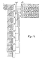
- the rotation circuit 41 may be constructed as shown in Fig. 11. In the rotation circuit 41 of Fig. 11, the input data bits al, a2, ---, a8 are rotated by the bit number determined by the control signal CNT from the control circuit 47, as Fig. 11 shows.
- the first selector circuit 43 in Fig. 9 may be constructed as shown in Fig. 12.
- first selector circuit 43 of Fig. 12 when the full signal FULL from the control circuit 47 is logic "low”, data from the second register circuit 45 is selected and is output to the second selector circuit 44.
- full signal FULL from the control circuit 47 is logic "high”, data from the first register circuit 42 is selected and is output to the second selector circuit 44.
- the second selector circuit 44 in Fig. 9 may be constructed as shown in Fig. 13.
- selection of either the data from the first selector circuit 43 or the data from the rotation circuit 41 is'carried out by the control signals Cl through C8 from the control circuit 47.
- the control signals Cl through C8 are determined in accordance with the bit number data in the converter circuit 474 of Fig. 9, as shown in Fig. 14.
- the data from the first selector circuit 43 is selected with regard to the bits from the top to the bit number in the register 472, and the data from the rotation circuit 41 is selected with regard to the remaining bits.
Landscapes
- Engineering & Computer Science (AREA)
- Signal Processing (AREA)
- Multimedia (AREA)
- Theoretical Computer Science (AREA)
- Compression, Expansion, Code Conversion, And Decoders (AREA)
Applications Claiming Priority (4)
| Application Number | Priority Date | Filing Date | Title |
|---|---|---|---|
| JP111445/82 | 1982-06-30 | ||
| JP57111445A JPS594255A (ja) | 1982-06-30 | 1982-06-30 | 可変長符号に対する符号変換回路 |
| JP111446/82 | 1982-06-30 | ||
| JP11144682A JPS593548A (ja) | 1982-06-30 | 1982-06-30 | 可変長符号の符号変換回路 |
Publications (3)
| Publication Number | Publication Date |
|---|---|
| EP0098153A2 true EP0098153A2 (fr) | 1984-01-11 |
| EP0098153A3 EP0098153A3 (en) | 1986-10-01 |
| EP0098153B1 EP0098153B1 (fr) | 1989-11-08 |
Family
ID=26450835
Family Applications (1)
| Application Number | Title | Priority Date | Filing Date |
|---|---|---|---|
| EP83303732A Expired EP0098153B1 (fr) | 1982-06-30 | 1983-06-28 | Circuit de conversion de données numériques pour un code de données à longueur de mot variable |
Country Status (4)
| Country | Link |
|---|---|
| US (1) | US4593267A (fr) |
| EP (1) | EP0098153B1 (fr) |
| CA (1) | CA1211219A (fr) |
| DE (1) | DE3380833D1 (fr) |
Cited By (10)
| Publication number | Priority date | Publication date | Assignee | Title |
|---|---|---|---|---|
| DE3404436A1 (de) * | 1983-02-14 | 1984-08-16 | Canon K.K., Tokio/Tokyo | Datenverarbeitungseinrichtung |
| GB2138604A (en) * | 1983-02-25 | 1984-10-24 | Canon Kk | Data decoding |
| EP0233096A1 (fr) * | 1986-01-13 | 1987-08-19 | General Electric Cgr S.A. | Procédé de formattage et de déformattage de données résultant du codage d'informations numériques à l'aide d'un code à longueur variable, et dispositif de mise en oeuvre |
| EP0353826A1 (fr) * | 1988-08-05 | 1990-02-07 | Telecommunications Radioelectriques Et Telephoniques T.R.T. | Dispositif de codage statistique pour fournir des mots de code comportant un nombre variable d'éléments binaires |
| EP0397686A4 (en) * | 1988-01-28 | 1991-01-23 | General Electric Company | Apparatus for efficiently packing data in a buffer |
| EP0279909A3 (fr) * | 1986-11-04 | 1992-01-22 | TELETTRA Telefonia Elettronica e Radio S.p.A. | Code à longeur variable et dispositifs pour transmission à haute fréquence |
| EP0390310A3 (fr) * | 1989-03-31 | 1992-06-03 | Ampex Systems Corporation | Dispositif d'augmentation de la densité des données |
| EP0492537A1 (fr) * | 1990-12-21 | 1992-07-01 | Matsushita Electric Industrial Co., Ltd. | Dispositif d'enregistrement d'information |
| EP0905609A3 (fr) * | 1997-09-30 | 2000-04-05 | Siemens Aktiengesellschaft | Dispositif régistre |
| EP1067694A3 (fr) * | 1999-07-09 | 2003-10-15 | Sarnoff Corporation | Compression de données |
Families Citing this family (55)
| Publication number | Priority date | Publication date | Assignee | Title |
|---|---|---|---|---|
| JPS6226561A (ja) * | 1985-07-26 | 1987-02-04 | Toshiba Corp | パ−ソナルコンピユ−タ |
| US4853969A (en) * | 1987-01-13 | 1989-08-01 | Recognition Equipment Incorporated | Quantized digital filter |
| US5057837A (en) * | 1987-04-20 | 1991-10-15 | Digital Equipment Corporation | Instruction storage method with a compressed format using a mask word |
| US5179680A (en) * | 1987-04-20 | 1993-01-12 | Digital Equipment Corporation | Instruction storage and cache miss recovery in a high speed multiprocessing parallel processing apparatus |
| US5045853A (en) * | 1987-06-17 | 1991-09-03 | Intel Corporation | Method and apparatus for statistically encoding digital data |
| US5243701A (en) * | 1987-09-17 | 1993-09-07 | Mitsubishi Denki Kabushiki Kaisha | Method of and system for processing data having bit length variable with modes of operation |
| US4954983A (en) * | 1987-10-13 | 1990-09-04 | Tektronix, Inc. | Data driver for multiple mode buffered processor-peripheral data transfer with selective return of data to processor |
| DE3736898A1 (de) * | 1987-10-30 | 1989-05-11 | Siemens Ag | Anordnung zur umsetzung von codewoertern unterschiedlicher breite in datenwoerter gleicher breite |
| US4823201A (en) * | 1987-11-16 | 1989-04-18 | Technology, Inc. 64 | Processor for expanding a compressed video signal |
| US4985700A (en) * | 1988-03-01 | 1991-01-15 | Canon Kabushiki Kaisha | Variable-length coding/decoding device |
| JPH01230125A (ja) * | 1988-03-10 | 1989-09-13 | Nec Corp | レジスタの部分的更新機能を持つデータ処理装置 |
| US4967196A (en) * | 1988-03-31 | 1990-10-30 | Intel Corporation | Apparatus for decoding variable-length encoded data |
| US4885584A (en) * | 1988-04-07 | 1989-12-05 | Zilog, Inc. | Serializer system with variable character length capabilities |
| US5119092A (en) * | 1988-11-22 | 1992-06-02 | Sharp Kabushiki Kaisha | Apparatus for encoding, decoding, and storing waveforms |
| US5237701A (en) * | 1989-03-31 | 1993-08-17 | Ampex Systems Corporation | Data unpacker using a pack ratio control signal for unpacked parallel fixed m-bit width into parallel variable n-bit width word |
| JP2504206B2 (ja) * | 1989-07-27 | 1996-06-05 | 三菱電機株式会社 | バスコントロ―ラ |
| JPH03145223A (ja) * | 1989-10-30 | 1991-06-20 | Toshiba Corp | 可変長符号復調装置 |
| JPH0799812B2 (ja) * | 1990-03-26 | 1995-10-25 | 株式会社グラフイックス・コミュニケーション・テクノロジーズ | 信号符号化装置および信号復号化装置、並びに信号符号化復号化装置 |
| JP3013381B2 (ja) * | 1990-03-28 | 2000-02-28 | ソニー株式会社 | 可変長データの復号装置 |
| JP2922571B2 (ja) * | 1990-04-05 | 1999-07-26 | キヤノン株式会社 | データ変換回路 |
| DE4017447A1 (de) * | 1990-05-30 | 1991-12-05 | Siemens Ag | Verfahren und anordnung zur umsetzung von codewoertern mit unterschiedlicher breite in datenwoerter gleicher breite |
| US5136290A (en) * | 1990-06-18 | 1992-08-04 | Bond James W | Message expansion decoder and decoding method for a communication channel |
| US5173695A (en) * | 1990-06-29 | 1992-12-22 | Bell Communications Research, Inc. | High-speed flexible variable-length-code decoder |
| KR0181471B1 (ko) * | 1990-07-27 | 1999-05-15 | 윌리암 피.브레이든 | 컴퓨터 데이타 경로배정 시스템 |
| US5857088A (en) * | 1991-10-24 | 1999-01-05 | Intel Corporation | System for configuring memory space for storing single decoder table, reconfiguring same space for storing plurality of decoder tables, and selecting one configuration based on encoding scheme |
| US5408628A (en) * | 1992-07-07 | 1995-04-18 | Odetics, Inc. | Solid state recorder with flexible width data bus utilizing lock mapping and error correction and detection circuits |
| US5351047A (en) * | 1992-09-21 | 1994-09-27 | Laboratory Automation, Inc. | Data decoding method and apparatus |
| US5343195A (en) * | 1992-12-18 | 1994-08-30 | Thomson Consumer Electronics, Inc. | Variable length codeword decoding apparatus |
| US5459850A (en) * | 1993-02-19 | 1995-10-17 | Conner Peripherals, Inc. | Flash solid state drive that emulates a disk drive and stores variable length and fixed lenth data blocks |
| US5615020A (en) * | 1993-05-13 | 1997-03-25 | Keith; Michael | System and method for fast huffman decoding |
| US5699544A (en) * | 1993-06-24 | 1997-12-16 | Discovision Associates | Method and apparatus for using a fixed width word for addressing variable width data |
| US5861894A (en) * | 1993-06-24 | 1999-01-19 | Discovision Associates | Buffer manager |
| JPH07107303A (ja) * | 1993-09-30 | 1995-04-21 | Nec Corp | ハフマン符号の復号化方法 |
| US5835960A (en) * | 1994-01-07 | 1998-11-10 | Cirrus Logic, Inc. | Apparatus and method for interfacing a peripheral device having a ROM BIOS to a PCI bus |
| CA2145379C (fr) * | 1994-03-24 | 1999-06-08 | William P. Robbins | Methode et dispositif d'adressage memoire |
| JP3541439B2 (ja) * | 1994-07-08 | 2004-07-14 | ソニー株式会社 | 信号変調方法及び装置、並びに信号復調装置及び方法 |
| US5572208A (en) * | 1994-07-29 | 1996-11-05 | Industrial Technology Research Institute | Apparatus and method for multi-layered decoding of variable length codes |
| EP0721285B1 (fr) * | 1995-01-09 | 2001-04-18 | Matsushita Electric Industrial Co., Ltd. | Appareil de codage numérique |
| US5793896A (en) * | 1995-03-23 | 1998-08-11 | Intel Corporation | Ordering corrector for variable length codes |
| US5748790A (en) * | 1995-04-05 | 1998-05-05 | Intel Corporation | Table-driven statistical decoder |
| US6119213A (en) * | 1995-06-07 | 2000-09-12 | Discovision Associates | Method for addressing data having variable data width using a fixed number of bits for address and width defining fields |
| US5548338A (en) * | 1995-06-07 | 1996-08-20 | News American Publishing, Inc. | Compression of an electronic programming guide |
| JP3645027B2 (ja) * | 1995-09-20 | 2005-05-11 | 松下電器産業株式会社 | 可変長データ送受信装置 |
| US5646618A (en) * | 1995-11-13 | 1997-07-08 | Intel Corporation | Decoding one or more variable-length encoded signals using a single table lookup |
| US5848195A (en) * | 1995-12-06 | 1998-12-08 | Intel Corporation | Selection of huffman tables for signal encoding |
| US5661758A (en) * | 1996-01-16 | 1997-08-26 | Long; Michael E. | Single cycle data encoding method and apparatus |
| US5821887A (en) * | 1996-11-12 | 1998-10-13 | Intel Corporation | Method and apparatus for decoding variable length codes |
| JP3580777B2 (ja) * | 1998-12-28 | 2004-10-27 | フラウンホーファー−ゲゼルシャフト・ツール・フェルデルング・デル・アンゲヴァンテン・フォルシュング・アインゲトラーゲネル・フェライン | オーディオ信号又はビットストリームの符号化又は復号化のための方法及び装置 |
| JPWO2003084077A1 (ja) * | 2002-03-25 | 2005-08-04 | アライドテレシスホールディングス株式会社 | 可変長/固定長データ変換方法及び装置 |
| US7136430B2 (en) * | 2003-03-31 | 2006-11-14 | Nortel Networks Limited | Digital receiver and method |
| US6987953B2 (en) * | 2003-03-31 | 2006-01-17 | Nortel Networks Limited | Digital transmitter and method |
| US7191200B2 (en) * | 2003-07-10 | 2007-03-13 | Silicon Integrated Systems Corporation | Method and apparatus for binary number conversion |
| US7071846B2 (en) * | 2004-02-24 | 2006-07-04 | Lucent Technologies Inc. | Analog decoding method and decoder |
| US11196594B2 (en) | 2019-02-28 | 2021-12-07 | Nokia Solutions And Networks Oy | Probabilistic signal shaping using multiple codebooks |
| US10824794B2 (en) * | 2019-04-08 | 2020-11-03 | Paypal, Inc. | Process for creating a fixed length representation of a variable length input |
Citations (1)
| Publication number | Priority date | Publication date | Assignee | Title |
|---|---|---|---|---|
| JPS5517259A (en) | 1978-07-21 | 1980-02-06 | Fuji Electric Co Ltd | Feed roller device for laying gas insulated conductor |
Family Cites Families (4)
| Publication number | Priority date | Publication date | Assignee | Title |
|---|---|---|---|---|
| FR2253415A5 (fr) * | 1973-12-04 | 1975-06-27 | Cii | |
| US4044347A (en) * | 1975-05-19 | 1977-08-23 | International Business Machines Corporation | Variable-length to fixed-length conversion of minimum-redundancy codes |
| US4250548A (en) * | 1979-01-02 | 1981-02-10 | Honeywell Information Systems Inc. | Computer apparatus |
| CA1156764A (fr) * | 1979-02-22 | 1983-11-08 | Amitabh Saran | Circuit pour condenser des mots de donnees de ongueur variable en mots de longueur fixe |
-
1983
- 1983-06-27 CA CA000431197A patent/CA1211219A/fr not_active Expired
- 1983-06-28 DE DE8383303732T patent/DE3380833D1/de not_active Expired
- 1983-06-28 EP EP83303732A patent/EP0098153B1/fr not_active Expired
- 1983-06-30 US US06/509,398 patent/US4593267A/en not_active Expired - Lifetime
Patent Citations (1)
| Publication number | Priority date | Publication date | Assignee | Title |
|---|---|---|---|---|
| JPS5517259A (en) | 1978-07-21 | 1980-02-06 | Fuji Electric Co Ltd | Feed roller device for laying gas insulated conductor |
Cited By (18)
| Publication number | Priority date | Publication date | Assignee | Title |
|---|---|---|---|---|
| DE3404436A1 (de) * | 1983-02-14 | 1984-08-16 | Canon K.K., Tokio/Tokyo | Datenverarbeitungseinrichtung |
| FR2541013A1 (fr) * | 1983-02-14 | 1984-08-17 | Canon Kk | Appareil de traitement de donnees et appareil d'archivage de donnees d'images |
| GB2138184A (en) * | 1983-02-14 | 1984-10-17 | Canon Kk | Data compression |
| US4819079A (en) * | 1983-02-14 | 1989-04-04 | Canon Kabushiki Kaisha | Data processing apparatus |
| GB2138604A (en) * | 1983-02-25 | 1984-10-24 | Canon Kk | Data decoding |
| EP0233096A1 (fr) * | 1986-01-13 | 1987-08-19 | General Electric Cgr S.A. | Procédé de formattage et de déformattage de données résultant du codage d'informations numériques à l'aide d'un code à longueur variable, et dispositif de mise en oeuvre |
| FR2600223A1 (fr) * | 1986-01-13 | 1987-12-18 | Thomson Cgr | Procede de formattage et de deformattage de donnees resultant du codage d'informations numeriques a l'aide d'un code a longueur variable, et dispositif de mise en oeuvre |
| US4739308A (en) * | 1986-01-13 | 1988-04-19 | Thomson-Cgr | Method for the formatting and unformatting of data resulting from the encoding of digital information using a variable length code and a device for using this method |
| EP0279909A3 (fr) * | 1986-11-04 | 1992-01-22 | TELETTRA Telefonia Elettronica e Radio S.p.A. | Code à longeur variable et dispositifs pour transmission à haute fréquence |
| EP0397686A4 (en) * | 1988-01-28 | 1991-01-23 | General Electric Company | Apparatus for efficiently packing data in a buffer |
| FR2635241A1 (fr) * | 1988-08-05 | 1990-02-09 | Trt Telecom Radio Electr | Dispositif de codage statistique pour fournir des mots de code comportant un nombre variable d'elements binaires |
| US5062125A (en) * | 1988-08-05 | 1991-10-29 | Telecommunications Radioelectriques Et Telephoniques | Statistic coding arrangement for producing code words comprising a variable number of bits |
| EP0353826A1 (fr) * | 1988-08-05 | 1990-02-07 | Telecommunications Radioelectriques Et Telephoniques T.R.T. | Dispositif de codage statistique pour fournir des mots de code comportant un nombre variable d'éléments binaires |
| EP0390310A3 (fr) * | 1989-03-31 | 1992-06-03 | Ampex Systems Corporation | Dispositif d'augmentation de la densité des données |
| EP0492537A1 (fr) * | 1990-12-21 | 1992-07-01 | Matsushita Electric Industrial Co., Ltd. | Dispositif d'enregistrement d'information |
| US5272528A (en) * | 1990-12-21 | 1993-12-21 | Matsushita Electric Industrial Co., Ltd. | Information recording apparatus |
| EP0905609A3 (fr) * | 1997-09-30 | 2000-04-05 | Siemens Aktiengesellschaft | Dispositif régistre |
| EP1067694A3 (fr) * | 1999-07-09 | 2003-10-15 | Sarnoff Corporation | Compression de données |
Also Published As
| Publication number | Publication date |
|---|---|
| CA1211219A (fr) | 1986-09-09 |
| DE3380833D1 (en) | 1989-12-14 |
| EP0098153B1 (fr) | 1989-11-08 |
| EP0098153A3 (en) | 1986-10-01 |
| US4593267A (en) | 1986-06-03 |
Similar Documents
| Publication | Publication Date | Title |
|---|---|---|
| EP0098153B1 (fr) | Circuit de conversion de données numériques pour un code de données à longueur de mot variable | |
| US5382955A (en) | Error tolerant thermometer-to-binary encoder | |
| US5436626A (en) | Variable-length codeword encoder | |
| US4468790A (en) | System for the quantization of signals | |
| EP0324584B1 (fr) | Dispositif de codage prédictif | |
| US3945002A (en) | Block digital processor for use with nonuniformly encoded digital words | |
| EP0490504A2 (fr) | Schéma de codage de ligne à plusieurs niveaux | |
| GB2049371A (en) | Modulating and demodulating binary data signals | |
| US4191858A (en) | Block digital processing system for nonuniformly encoded digital words | |
| US5146220A (en) | Data conversion method and apparatus for converting undefined length data to fixed length data | |
| HUP9902002A2 (hu) | Berendezés m-bites adatszósorozat modulált jellé való átalakítására | |
| US4882585A (en) | Method and apparatus for high resolution analog-digital-analog transformations | |
| US7071855B1 (en) | Gray code conversion method and apparatus embodying the same | |
| US4189715A (en) | μ-Law to floating point converter | |
| US4393367A (en) | Digital compandor having nonlinear companding characteristics | |
| EP0193592B1 (fr) | Procede et dispositif de traitement de signaux numeriques avant l'enregistrement | |
| EP0661820A2 (fr) | Circuit parallèle-série de conversion de données | |
| US6115424A (en) | Coding method of dividing information block serving as conversion unit into a plurality of sub-blocks to perform coding for each sub-block, and coding apparatus | |
| KR860001344B1 (ko) | 가변어장(Variable-Word-Length) 데이타 코우드용 디지탈 데이타 코우드 변환회로 | |
| US6816098B2 (en) | High-speed oversampling modulator device | |
| US6496602B2 (en) | Sorting device of variable-length code | |
| JPH04252329A (ja) | データを可変長ビットパターンで表す方法及び通信システム | |
| US5828906A (en) | System for sequentially shifting bits from the next one of the most significant bit and then outputting the most significant bit according a selection signal | |
| KR0182499B1 (ko) | 가변장 부호 변환장치 및 그 변환방법 | |
| SU1197086A1 (ru) | Система св зи с дельта-модул цией |
Legal Events
| Date | Code | Title | Description |
|---|---|---|---|
| PUAI | Public reference made under article 153(3) epc to a published international application that has entered the european phase |
Free format text: ORIGINAL CODE: 0009012 |
|
| AK | Designated contracting states |
Designated state(s): DE FR GB IT |
|
| RAP1 | Party data changed (applicant data changed or rights of an application transferred) |
Owner name: FUJITSU LIMITED Owner name: NIPPON TELEGRAPH AND TELEPHONE CORPORATION |
|
| PUAL | Search report despatched |
Free format text: ORIGINAL CODE: 0009013 |
|
| AK | Designated contracting states |
Kind code of ref document: A3 Designated state(s): DE FR GB IT |
|
| 17P | Request for examination filed |
Effective date: 19870313 |
|
| 17Q | First examination report despatched |
Effective date: 19880420 |
|
| GRAA | (expected) grant |
Free format text: ORIGINAL CODE: 0009210 |
|
| ITF | It: translation for a ep patent filed | ||
| AK | Designated contracting states |
Kind code of ref document: B1 Designated state(s): DE FR GB IT |
|
| REF | Corresponds to: |
Ref document number: 3380833 Country of ref document: DE Date of ref document: 19891214 |
|
| ET | Fr: translation filed | ||
| PLBE | No opposition filed within time limit |
Free format text: ORIGINAL CODE: 0009261 |
|
| STAA | Information on the status of an ep patent application or granted ep patent |
Free format text: STATUS: NO OPPOSITION FILED WITHIN TIME LIMIT |
|
| 26N | No opposition filed | ||
| ITTA | It: last paid annual fee | ||
| PGFP | Annual fee paid to national office [announced via postgrant information from national office to epo] |
Ref country code: FR Payment date: 20000612 Year of fee payment: 18 |
|
| PGFP | Annual fee paid to national office [announced via postgrant information from national office to epo] |
Ref country code: DE Payment date: 20000626 Year of fee payment: 18 |
|
| PGFP | Annual fee paid to national office [announced via postgrant information from national office to epo] |
Ref country code: GB Payment date: 20000628 Year of fee payment: 18 |
|
| PG25 | Lapsed in a contracting state [announced via postgrant information from national office to epo] |
Ref country code: GB Free format text: LAPSE BECAUSE OF NON-PAYMENT OF DUE FEES Effective date: 20010628 |
|
| GBPC | Gb: european patent ceased through non-payment of renewal fee |
Effective date: 20010628 |
|
| PG25 | Lapsed in a contracting state [announced via postgrant information from national office to epo] |
Ref country code: FR Free format text: LAPSE BECAUSE OF NON-PAYMENT OF DUE FEES Effective date: 20020228 |
|
| PG25 | Lapsed in a contracting state [announced via postgrant information from national office to epo] |
Ref country code: DE Free format text: LAPSE BECAUSE OF NON-PAYMENT OF DUE FEES Effective date: 20020403 |