EP0101201B1 - Dispositif à circuit intégré monolithique comprenant un circuit amplificateur haute fréquence du type à contre-réaction en courant alternatif - Google Patents
Dispositif à circuit intégré monolithique comprenant un circuit amplificateur haute fréquence du type à contre-réaction en courant alternatif Download PDFInfo
- Publication number
- EP0101201B1 EP0101201B1 EP83304191A EP83304191A EP0101201B1 EP 0101201 B1 EP0101201 B1 EP 0101201B1 EP 83304191 A EP83304191 A EP 83304191A EP 83304191 A EP83304191 A EP 83304191A EP 0101201 B1 EP0101201 B1 EP 0101201B1
- Authority
- EP
- European Patent Office
- Prior art keywords
- transistor
- negative feedback
- monolithic integrated
- integrated circuit
- high frequency
- Prior art date
- Legal status (The legal status is an assumption and is not a legal conclusion. Google has not performed a legal analysis and makes no representation as to the accuracy of the status listed.)
- Expired
Links
Images







Classifications
-
- H—ELECTRICITY
- H03—ELECTRONIC CIRCUITRY
- H03F—AMPLIFIERS
- H03F3/00—Amplifiers with only discharge tubes or only semiconductor devices as amplifying elements
- H03F3/45—Differential amplifiers
- H03F3/45071—Differential amplifiers with semiconductor devices only
-
- H—ELECTRICITY
- H03—ELECTRONIC CIRCUITRY
- H03F—AMPLIFIERS
- H03F1/00—Details of amplifiers with only discharge tubes, only semiconductor devices or only unspecified devices as amplifying elements
- H03F1/42—Modifications of amplifiers to extend the bandwidth
- H03F1/48—Modifications of amplifiers to extend the bandwidth of aperiodic amplifiers
-
- H—ELECTRICITY
- H03—ELECTRONIC CIRCUITRY
- H03F—AMPLIFIERS
- H03F3/00—Amplifiers with only discharge tubes or only semiconductor devices as amplifying elements
- H03F3/189—High-frequency amplifiers, e.g. radio frequency amplifiers
- H03F3/19—High-frequency amplifiers, e.g. radio frequency amplifiers with semiconductor devices only
Definitions
- This invention relates to a monolithic integrated circuit device including an AC negative feedback type high frequency amplifier circuit.
- circuit device when the circuit device is fabricated with the monolithic integrated circuit technique, it is extremely difficult to manufacture, at a high yield, devices having predetermined characteristic by preparing circuit element having predetermined values as in the prior art in which the circuit device is fabricated with discrete component elements.
- a device utilized in such high frequency band as several hundred MHz is fabricated with a monolithic integrated circuit, dimensional errors of various component elements of the device, nonuniformity of the semiconductor material utilized to form the device and a small misalignment of the mask have a great influence upon the characteristics of the completed device.
- an amplifier circuit utilized in a high frequency band higher than several hundred MHz nonuniformities described above greatly affect the frequency characteristic, thus decreasing the yield of satisfactory products.
- the principal object of this invention is to provide a monolithic integrated circuit device including an AC negative feedback type high frequency amplifier circuit having a desired wide bandwidth frequency characteristic.
- Another object of this invention is to provide a monolithic integrated circuit device having an AC negative feedback type high frequency amplifier capable of improving the yield of satisfactory products.
- a further object of this invention is to provide a monolithic integrated circuit device including an AC negative feedback type high frequency amplifier capable of externally adjusting the frequency characteristic.
- a negative feedback is used for the purpose of improving the frequency characteristic.
- an AC negative feedback is effective for widening the frequency bandwidth because it forms a peak on the high frequency side of the amplifier circuit, thus broadening the frequency bandwidth.
- the invention is based on this discovery.
- a monolithic integrated circuit device including a high frequency amplifier circuit provided with a negative feedback circuit, characterized by:
- US ⁇ A ⁇ 3671886 describes an automatic gain control circuit comprising a multi-stage variable equalizing network having variable reactance elements, including diodes, used in a PCM regenerative repeater in a transmission line.
- the variable reactance elements are automatically controlled so as to change the pole frequencies of each stage of the network in proportion to the square route of a frequency characteristic of a line loss.
- a solid line block 10 represents a monolithic integrated circuit wafer made of silicon, for example.
- An AC negative feedback type high frequency amplifier circuit often called a peaking amplifier is fabricated on the wafer by well known semiconductor technique.
- the high frequency amplifier circuit comprises, as its principal elements, an amplifier 12 which amplifies a high frequency input signal supplied from outside through a pad 11 a (external terminal) and outputs the amplified signal via a pad 11 b lexternal terminal) a stabilized source 13 supplying an operating power to the amplifier 12, and an AC negative feedback circuit 14 which adjusts the amount of the negative feedback and including a semiconductor impedance element.
- the amplifier 12 and the stabilized source 13 are grounded through a pad 11c (external terminal).
- the AC negative feedback circuit 14 is an element that characterizes this invention and one terminal of the semiconductor impedance element contained therein is connected to an external control device which control the amount of the AC feedback through a pad 11d (external terminal).
- the stabilized source 13 is connected to an external source through a pad 11e (external terminal).
- the AC negative feedback circuit 14 can be controlled from the outside of the semiconductor wafer on which the monolithic integrated circuit is fabricated. Moreover, by controlling the amount of the AC negative feedback, the frequency characteristic of the amplifier circuit can be improved. Especially, it is possible to widen the bandwidth in the high frequency band, thus enabling to obtain a monolithic integrated circuit device including an AC negative feedback type high frequency amplifier circuit having a desired wide band frequency characteristic. Since the amount of the AC negative feedback can be controlled from outside, such amount can be adjusted independently of the DC negative feedback quantity.
- any desired frequency characteristic can be obtained by adjusting the amount of the AC negative feedback. Consequently the percentage of rejection of the monolithic circuit per bit can be minimized measuring an improvement of the yield.
- Figs. 2, 5,7 and 8 show examples of the peaking amplifier circuit utilizing a diode as the semiconductor impedance element of the AC negative feedback quantity.
- the amplifier 12 is constituted by a NPN transistor 31, a load resistor 32 with one end connected to the collector electrode of the transistor 31, and an emitter resistor 33 (that is a DC negative feedback resistor) with one end connected to the emitter electrode of the transistor.
- the base electrode of transistor 31 is supplied with an input signal via pad 11a, while the collector electrode sends out an output signal via pad 11 b.
- the other end of the load resistor 32 is connected to the stabilized source 13 shown by (+V), while the other end of the emitter resistor 33 is grounded through pad 11c.
- the emitter electrode of the transistor 31 is connected to the cathode electrode of a diode 41 constituting a semiconductor impedance element of the AC negative feedback circuit 14.
- the anode electrode of diode 41 is connected to an external control device 20 for controlling the AC negative feedback quantity via pad 11d.
- the control device 20 comprises a variable voltage source for applying a variable reverse bias to the diode 41, and the other end of the control device 20 is grounded. Accordingly, the junction capacitance of the diode under reverse bias is utilized as the AC impedance.
- a desired amount of the AC negative feedback can be applied to the amplifier 12 independently of the amount of the DC negative feedback provided by the emitter resistor.
- the junction capacitance of the diode 41 varies in accordance with the magnitude of the reverse bias voltage Vc.
- Fig. 3 shows the relation between the reverse bias voltage Vc and the junction capacitance when the junction area of the first and second semiconductor regions constituting the junction capacitance is 100 microns 2, the impurity concentration of the first semiconductor region is about 10 20 atoms/cm 3 , the impurity concentration of the second semiconductor region is 1018 atoms/cm 3 .
- AC negative feedback function is, when defined strictly, performed by the AC negative feedback circuit 14 in cooperation with the DC feedback circuit which is constituted by a pure resistor 33 such as emitter resistor.
- the AC negative feedback operation of the DC feedback circuit 33 is neglected since the DC feedback circuit does not have significant effect on the frequency characteristic, particularly the peaking characteristic of the high frequency amplifier circuit.
- Fig. 5 shows a connection diagram in which the high frequency circuit is modified to a differential type, in which elements corresponding to those shown in Fig. 1 are designated by the same reference numeral added with suffixes A and B.
- the circuit shown in Fig. 5 is different from that shown in fig. 1 in that a current source 35 is connected between the juncture between the emitter resistors 33A and 33B and the pad 11c.
- first and second diodes 41A and 41 B connected to apply a negative bias between the emitter electrodes of transistors 31 A and 31B and the pad lid.
- the control device 20 supplies a predetermined reverse bias voltage to the diodes 41A and 41 B via pad 11d.
- Fig. 6 shows the frequency characteristics of the high frequency amplifier circuit shown in Fig. 5 in which the abscissa represents the frequency, while the ordinate voltage gain.
- a dotted line curve shows the frequency characteristic where no AC negative feedback circuit is used.
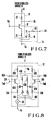
- Fig. 7 shows an improvement of the circuit shown in Fig. 2 in which corresponding circuit elements are designated by the same reference characters.
- the AC negative feedback circuit 14 connected to the emitter electrode of transistor 31 comprises a fixed capacitor 42, a diode 41 and a resistor 43.
- One end of the fixed capacitor 42 is connected to the emitter electrode of the transistor 31, while the other end is connected to the pad 11 d via the resistor 43 and to the pad 11c via diode 41.
- a serial combination of capacitor 42 and diode 41 is connected in parallel with the emitter resistor 33 for DC feedback.
- the juncture between the capacitor 42 and the diode 41 is connected to a control device for adjusting the amount of the AC negative feedback via resistor 43 and pad 11d.
- the anode electrode of diode 41 is connected to pad 11c so that the junction capacitance thereof can be used at the time of reverse bias.
- the equivalent peaking capacitance Cp is given by the following equation:
- the AC negative feedback circuit 14 is isolated (in terms of DC) from the emitter electrode of the transistor 31 so that it is not necessary to change the reverse bias voltage applied to the pad 11d when the bias condition of the transistor 31 varies.
- Fig. 8 shows an improvement of the circuit shown in Fig. 5 in which elements corresponding to those shown in Fig. 5 are designated by the same reference characters.
- the AC negative feedback circuit connected to the emitter electrodes of transistors 31A and 31B has the same construction as that shown in Fig. 7. More particularly, between the emitter electrode of transistor 31A and the pad 11c are connected in series a capacitor 42A and a diode 41A, and a resistor 43A is connected between the juncture between the capacitor 42A and diode 41 A and pad 11d connected to the control device 20.
- serially connected capacitor 42B and a diode 41B are connected between the emitter electrode of transistor 31B and pad 11c and resistor 43B is connected between the junction between capacitor 42B and diode 41 B and pad 11a.
- a predetermined reverse bias voltage is applied to the cathode of the first and second diodes 41A and 41 B from the pad 11d via resistors 43A and 43B respectively.
- Figs. 9 through 25 show other examples of the monolithic integrated circuit embodying the invention in which the diffusion capacitance of a transistor is used as a semiconductor impedance that adjusts the amount of AC negative feedback.
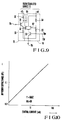
- the amplifier 12 is made up of an NPN transistor 31, a load resistor 32, and an emitter resistor 33 acting as a DC negative feedback resistor, in the same manner as in the previous embodiment.
- the base electrode of transistor 31 is supplied with an input signal via pad 11 a to send out an output signal from the collector electrode via pad 11 b.
- the AC negative feedback circuit 14 characterizing the invention comprises an NPN transistor 51 acting as an AC negative feedback semiconductor impedance element.
- the diffusion capacitance between the base and emitter electrodes of the transistor 51 is used as the peaking capacitance. Since the impedance of the transistor 53 acting as a current source as seen from transistor 51 is high, a transistor 52 is connected in parallel with transistor 51 to operate as a common base circuit type to decrease the AC impedance.
- the base electrode of transistor 51 is connected to the emitter electrode of transistor 31, and the emitter electrodes of transistor 51 and of NPN transistor 52 are grounded via pad 11c and an NPN transistor 53, whereby the diffusion capacitance between the base and emitter electrodes of transistor 51 acts as the peaking capacitance.
- the collector electrodes of transistors 51 and 52 are connected to the stabilized source 13 to be applied with a voltage of +V resistors 54 and 55 act as bias resistors for transistor 52.
- the peaking capacitance Cpc is approximately given by (g m ' ⁇ F )/h FE (diffusion capacitance between the base and emitter electrodes) where gm represents the mutual conductance of transistor 51 and TF the forward base transit time of minority carriers, and where it is assumed that the junction capacitance is sufficiently small. Since the mutual conductance gm is expressed by (where K is a Boltzmann constant, T the absolute temperature, q electric quantity and Ip current flowing through transistor 51), the peaking capacitance Cpc would be expressed by
- the purpose of the peaking control transistor 53 is to control the current Ip flowing through the transistor 51. Further, it is possible to control the current Ip by varying the voltage Vpc applied to the control device 20 via the base electrode 53 and pad 11d d acting as the peaking control terminal.
- any desired peaking characteristic can be obtained, thereby broadening the frequency bandwidth of the amplifier circuit.
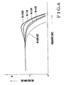
- Fig. 11 shows a voltage gain-frequency characteristics of the circut shown in Fig. 9 wherein the voltage Vpc applied to the base electrode of the transistor 53 from the control device 20 was varied between 0 V and 0.84 V.
- the characteristics shown in Fig. 11 were obtained with element having the following values.
- Fig. 12 shows a modification of Fig. 9 which is different in that the connection of the emitter and collector electrodes of transistor 52 are reversed.
- the stabilized source 13 has a voltage lower than that applied to the pad 11c.
- the diffusion capacitance between the base and collector electrodes of transistor 51 is used as the negative feedback semiconductor impedance of the AC negative feedback circuit.
- the circuit shown in Fig. 12 operates in the same manner as in Fig. 9, but the reverse direction peaking capacitance Cpc is expressed by (where TR represents the reverse base transit time) which is given by the base collector diffusion capacitance.
- TR represents the reverse base transit time
- the circuit shown in Fig. 12 since TR » TF it is possible to obtain larger peaking capacitance, and the voltage gain is given by equation (1) described above except that TF is replaced by TR .
- the circuit shown in Fig. 12 has the same advantages as those of the circuit shown in Fig. 8.
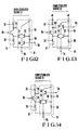
- Fig. 13 shows a modification of Fig. 9 different therefrom in that transistors 51, 52 and 53 are substituted by PNP transistors and that the transistor 53 acting as the current source is disposed on the collector side of a transistor pair 51 and 52. Since the circuit shown in Fig. 13 operates in the same manner as in Fig. 9, it will not be described herein.
- Fig. 14 shows a modification of Fig. 13 which is different therefrom in that the connections of collector and emitter electrodes of transistors 51 and 52 are reversed so as to utilize the base-collector diffusion capacitance of the transistor 51 as the negative feedback semiconductor impedance element.
- the circuit shown in Fig. 14 operates in the same manner as in Fig. 12.
- Fig. 15 shows still another embodiment of this invention which it differs from Fig. 9 in that the current Ip flowing through transistor 51 is controlled according to different method.
- the AC negative feedback circuit 14 comprises a negative feedback semiconductor impedance element.
- This impedance element comprises transistors 51 and 54 with their collector and emitter electrodes interconnected, and a constant current circuit 55 connected between the emitter electrode of transistor 51 and pad 11c.
- the control device 20 is connected to the base electrode of transistor 54 via pad 11d, and the collector electrode of transistor 54 is connected to the stabilized source 13.
- the current flowing through the transistor 54 is controlled by the voltage supplied from the control device 20 via pad 11d for controlling the current Ip flowing through complemental transistors.
- Other operations are identical to those of Fig. 9.
- Fig. 16 shows still another embodiment of this invention which is different from that shown in Fig. 15 in that transistor 51 and the AC negative feedback control transistor 54 are operated oppositely. Other points are the same as in Fig. 15.
- Fig. 17 shows yet another embodiment of this invention which is different from that shown in Fig. 15 in that the NPN transistor 51 and the NPN AC negative feedback control transistor 54 shown in Fig. 16 are substituted by PNP transistors.
- the constant current source 55 is connected between the collector electrodes of transistors 51 and 54 and the stabilized source 13. This modification too operates in the same manner as in the amplifier circuit shown in Fig. 15.
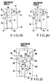
- the transistors 51 and 54 shown in Fig. 17 are operated oppositely, the other construction being the same as in Fig. 17.
- the collector electrode of transistor 51 is connected to the stabilized source 13 via a resistor 56.
- the collector electrode of a transistor 57 is connected to the collector electrode of transistor 51, while the emitter electrode of transistor 57 is connected to the stabilized source 13.
- the modification shown in Fig. 20 is different from that shown in Fig. 19 in that the transistor 51 is operated reversely but operates in the same manner.
- Fig. 21 shows a still further modification of this invention which is suitable for use as a differential type high frequency amplifier circuit.
- elements corresponding to those shown in Fig. 9 are designated by the same reference numerals added with suffixes A and B.
- a current source 35 is connected between the junction between the emitter resistors 33A and 33B and the pad 11c.
- the semiconductor impedance element of the AC negative feedback circuit 14 is used as the semiconductor impedance element of the AC negative feedback circuit 14 .
- the diffusion capacitance between the base-emitter electrodes of NPN transistor pair 51A and 51 B The collector electrodes of these transistors are connected to the stabilized source 13 while the emitter electrodes are connected to the grounded pad 11c via an NPN transistor 53 acting as a current source.
- the base electrode of transistor 53 is connected to the pad 11d receiving the control voltage from the control device 2a.
- the base-emitter diffusion capacitances of transistors 51A and 51 B of the AC negative feedback circuit 14 are connected in series and both ends of the capacitance are connected to the emitter electrodes of the transistors 31A and 31B.
- the peaking capacitance that is the sum Cpc of both diffusion capacitances can be approximately expressed by when it is assumed that the both diffusion capacitances are equal.
- the purpose of transistor 53 is to control the current Ip flowing through the transistor pair 51A and 51B and by varying the voltage Vpc impressed upon the pad 11 d, the current Ip can be varied for obtaining any desired peaking characteristic.
- Fig. 22 shows the relationship between the voltage gain (dB) and the frequency in GHz.
- the value R L of the load resistor 32 of the high frequency amplifier circuit is 1 K ohm
- the resistance value R E of the DC negative feedback resistor 33 is 450 ohms
- the emitter current Ip flowing through the DC negative feedback resistor is 2 mA and when the control voltage applied to the pad 11 from the variable control device 20 is varied between 0 and 3.5 V.
- the dotted line shown in Fig. 22 shows a characteristic when no AC negative feedback circuit is provided.
- Fig. 23 shows a modification of Fig. 21 which is different therefrom in that transistors 51A and 51 B are operated reversely, and the base-collector diffusion capacitances of transistor pair 51A and 51 B are used as the diffusion capacitance.
- This modification operates in the same manner as in Fig. 21.
- Fig. 24 shows still another modification of this invention similar to that shown in Fig. 21 except that PNP transistors are used instead of NPN transistors 51A and 51B and the AC negative feedback controlling NPN transistor 43.
- the emitter electrodes of the transistor pair 51A and 51 B are connected directly to pad 11c and the collector electrodes are connected to the stabilized source 13 via a PNP transistor 53 acting as a current source.
- the base electrode of transistor 53 is connected to pad 11d supplied with the control voltage V oc from the control device.
- the operation and advantages of this modification are similar to those of the embodiment shown in Fig. 21.
- Fig. 25 shows a modification of Fig. 24 in which the AC negative feedback transistor pair 51A and 51B are operated reversely. This modification operates in the same manner as that shown in Fig. 23.
- Figs. 26 through 34 show other embodiments in which a differentiated resistance of a diode is used as the semiconductor impedance element for adjusting the amount of AC negative feedback.
- Fig. 26 shows the principle of the AC negative feedback circuit 14 which is applied to the high frequency amplifier circuit shown in Fig. 2 or 5.
- the AC negative feedback circuit 14 shown in Fig. 26 comprises a fixed capacitor 61 for DC interruption with one terminal T1 connected to the emitter electrode of transistor 31 (Fig. 2) of the high frequency amplifier circuit, and serially connected diode 62 and a variable current source 63 controlled by an external input signal.
- the other end of capacitor 61 is connected to the juncture between the diode 62 and the current source 63.
- the anode terminal T2 is connected to a stabilized source, for example while the terminal T3 is grounded.
- the AC negative feedback circuit 64 of this construction is shown by an equivalent AC circuit shown in Fig.
- the differentiated resistance R D of the diode 62 can be varied as shown in Fig. 28 by varying the bias current.
- Equation (2) The value of product R D . C D in equation (2) is determined by the cut off frequency of the diode and is always constant irrespective of the operating current I D so that the frequency characteristic of the impedance shown by equation (2) can be shown by Fig. 29. Thus it has poles w1 and w3 determined by 0 and product R D C D and a zero point determined by R D (C p +C D ). The poles w1 and w2 are fixed irrespective of the operating current I D of the diode 62, and pole w2 can be varied between two poles w1 and w2 by properly selecting Cp or by adding adjusted current I D to R o .
- Fig. 30 shows a modification of the circuit shown in Fig. 26 in which the connection of the variable current source 63 and the diode 62 is reversed. This modification also operates in the same manner as that shown in Fig. 26 with the same advantage.
- Figs. 31 and 32 show the frequency characteristic in a case where a DC feedback resistor RE of the high frequency circuit is connected in parallel with a AC feedback circuit.
- Fig. 31 is plotted taking the current I D as the parameter while Fig. 32 is plotted taking capacitance Cp as the parameter. These characteristics are plotted with a resistor R, of 80 ohms, and the forward base transit time ⁇ F of the diode of 25 ps.
- Fig. 31 shows that the impedance of the flat portion can be independently adjusted with current I D , and that the point at which the impedance begins to decrease, that is the pole does not vary appreciably even when current I D is changed.
- Fig. 31 shows that the impedance of the flat portion can be independently adjusted with current I D , and that the point at which the impedance begins to decrease, that is the pole does not vary appreciably even when current I D is changed.
- Figs. 33 and 34 show applications wherein the AC negative feedback circuit that utilizes the differentiated resistance of the diode shown in Fig. 26 as the AC negative feedback semiconductor impedance element is incorporated into an actual high frequency circuit.
- the amplifier 12 shown in Fig. 33 is constituted by a transistor 31, a load resistor 32, and a DC negative feedback resistor 33.
- An input signal is supplied to the base electrode of transistor 31 via pad 11 a from outside of the monolithic integrated circuit to send out an output to the outside of the monolithic integrated circuit from the collector electrode of the transistor 31 via pad 11 b.
- the collector electrode of transistor 31 is connected to the stabilized source via resistor 32, which the emitter electrode is connected to pad 11c of the monolithic integrated circuit, which is grounded.
- the AC negative feedback circuit 14 shown in Fig. 33 is connected to the emitter electrode of transistor 31. More particularly, the emitter electrode of transistor 31 is connected to one terminal of a capacitor 61, which the other terminal thereof is connected to the junction between a diode 62 and the collector electrode of a NPN transistor 63 that constitutes a variable current source. The electrode of the diode 62 is connected to the stabilized source. The emitter electrode of transistor 63 is connected to pad 11 c , while the base electrode is connected to receive a control voltage from an external AC negative feedback quantity control device 20 via pad 11d of the monolithic integrated circuit.
- the gain G of the amplifier circuit is expressed by the following equation (3) where Z represents the impedance of the AC negative feedback circuit expressed by equation (2).
- the parallel impedance RE and the impedance Z of the denominator provide the frequency characteristic shown in Figs. 31 and 32. Consequently, the frequency characteristic of the gain G becomes the reciprocal of the impedance of the denominator, that is the peaking characteristic.
- the frequency at which the peaking begins can be set by the setting of Cp independently of the DC bias characteristic.
- the amount of peaking can be freely adjusted independently of the DC bias characteristic and the peaking initiation frequency by the current I D .
- Fig. 34 shows one example of application of the AC negative feedback circuit shown in Fig. 26 to a differential by the high frequency amplifier circuit.
- circuit elements corresponding to those shown in Fig. 30 are designed by the same reference characters added with suffixes A and B.
- Fig. 34 there is added a current source 35 connected between the junction between the emitter resistors 33A and 33B and the pad 11 c .
- two sets of elements constituting the AC negative feedback circuit shown in Fig. 30 are used which are respectively connected to the emitter electrodes of transistors 31A and 31 B.
- the base electrodes of transistors 63A and'63B acting as variable current sources are commonly connected to the external control device 20 via pad 11 d .
- the peaking characteristic of the high frequency amplifier circuit can be adjusted as desired by proper selection of the capacitances of capacitor 61A and 61B, and by controlling R D through an external terminal.
- the impedance by using a capacitor and the differentiated resistance of a diode and by varying the current bias condition of this diode.
- the peaking initiation frequency and the degree of peaking can be adjusted or set independently.
- the degree of peaking can be adjusted by observing the characteristic, thus obtaining a stable amplifier characteristic. This improves, the yield and decreases the manufacturing cost so that the frequency band can be widened as far as possible.
- the transistor comprising the amplifier of the high frequency amplifier circuit may be of PNP type instead of NPN type.
- the amplifier may be constituted by multi-stage transistors.
- a stabilized source circuit is formed on a semiconductor integrated circuit substrate ..., this is not material to this invention. If the voltage source supplied is sufficiently stabilized an independent stabilized source can be omitted.
- the stabilized source circuit may be formed on the outside of the substrate.
- control device was formed independently of the integrated circuit incorporated with an amplifier, but a portion of the control device, for example a temperature characteristic compensation circuit, may be incorporated into the integrated circuit including the amplifier, while a control element such as a variable resistor may be formed on the outside.
- the diode can be obtained from a transistor by connecting its base and collector or alternatively by floating its collector so that a junction between the base and emitter takes part in the diode function.
Landscapes
- Engineering & Computer Science (AREA)
- Power Engineering (AREA)
- Amplifiers (AREA)
Claims (18)
les autres électrodes de sortie des premier et second transistors sont normalement connectées à ladite source de courant (55),
et dans lequel ledit circuit de contre-réaction en courant alternatif (14) comporte:
Applications Claiming Priority (6)
| Application Number | Priority Date | Filing Date | Title |
|---|---|---|---|
| JP57125366A JPS5916404A (ja) | 1982-07-19 | 1982-07-19 | 増幅回路 |
| JP125366/82 | 1982-07-19 | ||
| JP137195/82 | 1982-08-09 | ||
| JP13719582A JPS5927612A (ja) | 1982-08-09 | 1982-08-09 | 増幅回路 |
| JP141984/82 | 1982-08-16 | ||
| JP14198482A JPS5932209A (ja) | 1982-08-16 | 1982-08-16 | 増幅回路 |
Publications (3)
| Publication Number | Publication Date |
|---|---|
| EP0101201A2 EP0101201A2 (fr) | 1984-02-22 |
| EP0101201A3 EP0101201A3 (en) | 1986-08-27 |
| EP0101201B1 true EP0101201B1 (fr) | 1990-03-28 |
Family
ID=27315110
Family Applications (1)
| Application Number | Title | Priority Date | Filing Date |
|---|---|---|---|
| EP83304191A Expired EP0101201B1 (fr) | 1982-07-19 | 1983-07-19 | Dispositif à circuit intégré monolithique comprenant un circuit amplificateur haute fréquence du type à contre-réaction en courant alternatif |
Country Status (4)
| Country | Link |
|---|---|
| US (1) | US4542350A (fr) |
| EP (1) | EP0101201B1 (fr) |
| CA (1) | CA1201775A (fr) |
| DE (1) | DE3381390D1 (fr) |
Families Citing this family (10)
| Publication number | Priority date | Publication date | Assignee | Title |
|---|---|---|---|---|
| EP0176069A1 (fr) * | 1984-09-24 | 1986-04-02 | Siemens Aktiengesellschaft | Filtre passe-haut avec amplificateur |
| US4705946A (en) * | 1985-09-05 | 1987-11-10 | Hughes Aircraft Company | Infrared sensor comprising improved feedback limited amplifier and associated method for amplifying electronic signals |
| GB8608087D0 (en) * | 1986-04-02 | 1986-05-08 | Plessey Co Plc | Variable resistors |
| US4703285A (en) * | 1986-04-23 | 1987-10-27 | Tektronix, Inc. | Wideband amplifier with active high-frequency compensation |
| FR2646574B1 (fr) * | 1989-04-28 | 1991-07-05 | Alcatel Transmission | Amplificateur a gain reglable, utilisable dans le domaine des hyperfrequences |
| US5039952A (en) * | 1990-04-20 | 1991-08-13 | International Business Machines Corp. | Electronic gain cell |
| US6175279B1 (en) * | 1997-12-09 | 2001-01-16 | Qualcomm Incorporated | Amplifier with adjustable bias current |
| US6490174B1 (en) * | 2001-06-04 | 2002-12-03 | Honeywell International Inc. | Electronic interface for power stealing circuit |
| JP4544947B2 (ja) * | 2004-09-15 | 2010-09-15 | 三菱電機株式会社 | 増幅回路 |
| JP4077831B2 (ja) * | 2005-05-11 | 2008-04-23 | 松下電器産業株式会社 | 高周波増幅器 |
Family Cites Families (5)
| Publication number | Priority date | Publication date | Assignee | Title |
|---|---|---|---|---|
| GB838731A (en) * | 1957-09-05 | 1960-06-22 | Ferguson Radio Corp | Improvements in or relating to transistor circuits |
| US3524141A (en) * | 1968-08-26 | 1970-08-11 | Rca Corp | Transistor amplifier having emitter bypass through an auxiliary transistor |
| JPS527304B1 (fr) * | 1969-08-29 | 1977-03-01 | ||
| DE2347711C2 (de) * | 1973-09-21 | 1975-10-02 | Siemens Ag, 1000 Berlin Und 8000 Muenchen | Transistorbreitbandverstärker |
| NL7409191A (nl) * | 1974-07-08 | 1976-01-12 | Philips Nv | Verschilversterker. |
-
1983
- 1983-07-18 CA CA000432581A patent/CA1201775A/fr not_active Expired
- 1983-07-19 US US06/515,280 patent/US4542350A/en not_active Expired - Fee Related
- 1983-07-19 EP EP83304191A patent/EP0101201B1/fr not_active Expired
- 1983-07-19 DE DE8383304191T patent/DE3381390D1/de not_active Expired - Lifetime
Also Published As
| Publication number | Publication date |
|---|---|
| EP0101201A2 (fr) | 1984-02-22 |
| DE3381390D1 (de) | 1990-05-03 |
| EP0101201A3 (en) | 1986-08-27 |
| US4542350A (en) | 1985-09-17 |
| CA1201775A (fr) | 1986-03-11 |
Similar Documents
| Publication | Publication Date | Title |
|---|---|---|
| US6046642A (en) | Amplifier with active bias compensation and method for adjusting quiescent current | |
| EP1744448B1 (fr) | Amplificateur radiofréquences | |
| US4275362A (en) | Gain controlled amplifier using a pin diode | |
| US4042886A (en) | High input impedance amplifier circuit having temperature stable quiescent operating levels | |
| SU528894A3 (ru) | Усилитель тока | |
| US4379268A (en) | Differential amplifier circuit | |
| US4395643A (en) | Broadband circuit with rapidly variable resistor | |
| US4542350A (en) | Monolithic integrated circuit device including AC negative feedback type high frequency amplifier circuit | |
| US4242598A (en) | Temperature compensating transistor bias device | |
| JP3390093B2 (ja) | 差動増幅器 | |
| GB2064253A (en) | Controllable-gain mixer circuit | |
| US6411170B2 (en) | Oscillation circuit | |
| US4172238A (en) | Differential amplifiers | |
| US4496908A (en) | Negative feedback amplifier having GaAs FET's | |
| US7154330B2 (en) | Stability compensation for adjustable gain amplifier | |
| US4207537A (en) | Differential field effect transistor amplifier having a compensating field effect transistor current source | |
| US4573022A (en) | Semiconductor integrated circuit using vertical PNP transistors | |
| US3996524A (en) | Linear amplifier utilizing adaptive biasing | |
| US2855468A (en) | Transistor stabilization circuits | |
| US4825173A (en) | High gain, programmable differential amplifier circuitry | |
| US20050184806A1 (en) | High frequency amplifier circuit | |
| US3487324A (en) | Plural channel amplifier system having variable feedback means | |
| US4481480A (en) | Feedback amplifier having a voltage-controlled compensation circuit | |
| EP1261124A1 (fr) | Un étage amplificateur à gain variable | |
| GB2066600A (en) | Variable-gain differential amplifier with gain-control-signal-independant dc output level |
Legal Events
| Date | Code | Title | Description |
|---|---|---|---|
| PUAI | Public reference made under article 153(3) epc to a published international application that has entered the european phase |
Free format text: ORIGINAL CODE: 0009012 |
|
| AK | Designated contracting states |
Designated state(s): DE FR GB NL |
|
| RAP1 | Party data changed (applicant data changed or rights of an application transferred) |
Owner name: NIPPON TELEGRAPH AND TELEPHONE CORPORATION |
|
| PUAL | Search report despatched |
Free format text: ORIGINAL CODE: 0009013 |
|
| AK | Designated contracting states |
Kind code of ref document: A3 Designated state(s): DE FR GB NL |
|
| 17P | Request for examination filed |
Effective date: 19860905 |
|
| 17Q | First examination report despatched |
Effective date: 19880718 |
|
| GRAA | (expected) grant |
Free format text: ORIGINAL CODE: 0009210 |
|
| AK | Designated contracting states |
Kind code of ref document: B1 Designated state(s): DE FR GB NL |
|
| REF | Corresponds to: |
Ref document number: 3381390 Country of ref document: DE Date of ref document: 19900503 |
|
| ET | Fr: translation filed | ||
| PLBE | No opposition filed within time limit |
Free format text: ORIGINAL CODE: 0009261 |
|
| STAA | Information on the status of an ep patent application or granted ep patent |
Free format text: STATUS: NO OPPOSITION FILED WITHIN TIME LIMIT |
|
| 26N | No opposition filed | ||
| PGFP | Annual fee paid to national office [announced via postgrant information from national office to epo] |
Ref country code: FR Payment date: 19930423 Year of fee payment: 11 |
|
| PGFP | Annual fee paid to national office [announced via postgrant information from national office to epo] |
Ref country code: GB Payment date: 19930513 Year of fee payment: 11 |
|
| PGFP | Annual fee paid to national office [announced via postgrant information from national office to epo] |
Ref country code: NL Payment date: 19930731 Year of fee payment: 11 |
|
| PGFP | Annual fee paid to national office [announced via postgrant information from national office to epo] |
Ref country code: DE Payment date: 19930823 Year of fee payment: 11 |
|
| PG25 | Lapsed in a contracting state [announced via postgrant information from national office to epo] |
Ref country code: GB Effective date: 19940719 |
|
| PG25 | Lapsed in a contracting state [announced via postgrant information from national office to epo] |
Ref country code: NL Effective date: 19950201 |
|
| GBPC | Gb: european patent ceased through non-payment of renewal fee |
Effective date: 19940719 |
|
| NLV4 | Nl: lapsed or anulled due to non-payment of the annual fee | ||
| PG25 | Lapsed in a contracting state [announced via postgrant information from national office to epo] |
Ref country code: FR Effective date: 19950331 |
|
| PG25 | Lapsed in a contracting state [announced via postgrant information from national office to epo] |
Ref country code: DE Effective date: 19950401 |
|
| REG | Reference to a national code |
Ref country code: FR Ref legal event code: ST |