EP0101853A2 - Dispositif de délivrance de signaux à isolement galvanique pour un système de commande - Google Patents
Dispositif de délivrance de signaux à isolement galvanique pour un système de commande Download PDFInfo
- Publication number
- EP0101853A2 EP0101853A2 EP83106800A EP83106800A EP0101853A2 EP 0101853 A2 EP0101853 A2 EP 0101853A2 EP 83106800 A EP83106800 A EP 83106800A EP 83106800 A EP83106800 A EP 83106800A EP 0101853 A2 EP0101853 A2 EP 0101853A2
- Authority
- EP
- European Patent Office
- Prior art keywords
- converter
- output
- control system
- optocouplers
- identification signal
- Prior art date
- Legal status (The legal status is an assumption and is not a legal conclusion. Google has not performed a legal analysis and makes no representation as to the accuracy of the status listed.)
- Granted
Links
- 238000002955 isolation Methods 0.000 claims description 3
- 238000012545 processing Methods 0.000 abstract description 8
- 238000000034 method Methods 0.000 abstract description 4
- 238000011143 downstream manufacturing Methods 0.000 abstract 1
- 238000000926 separation method Methods 0.000 abstract 1
- 238000004804 winding Methods 0.000 description 4
- 230000006399 behavior Effects 0.000 description 2
- 239000003990 capacitor Substances 0.000 description 2
- 238000013461 design Methods 0.000 description 2
- 238000012544 monitoring process Methods 0.000 description 2
- 238000010586 diagram Methods 0.000 description 1
- 230000007257 malfunction Effects 0.000 description 1
- 230000005693 optoelectronics Effects 0.000 description 1
- 230000005855 radiation Effects 0.000 description 1
- 238000012546 transfer Methods 0.000 description 1
Images
Classifications
-
- H—ELECTRICITY
- H04—ELECTRIC COMMUNICATION TECHNIQUE
- H04B—TRANSMISSION
- H04B10/00—Transmission systems employing electromagnetic waves other than radio-waves, e.g. infrared, visible or ultraviolet light, or employing corpuscular radiation, e.g. quantum communication
- H04B10/80—Optical aspects relating to the use of optical transmission for specific applications, not provided for in groups H04B10/03 - H04B10/70, e.g. optical power feeding or optical transmission through water
- H04B10/801—Optical aspects relating to the use of optical transmission for specific applications, not provided for in groups H04B10/03 - H04B10/70, e.g. optical power feeding or optical transmission through water using optical interconnects, e.g. light coupled isolators, circuit board interconnections
- H04B10/802—Optical aspects relating to the use of optical transmission for specific applications, not provided for in groups H04B10/03 - H04B10/70, e.g. optical power feeding or optical transmission through water using optical interconnects, e.g. light coupled isolators, circuit board interconnections for isolation, e.g. using optocouplers
-
- H—ELECTRICITY
- H03—ELECTRONIC CIRCUITRY
- H03K—PULSE TECHNIQUE
- H03K17/00—Electronic switching or gating, i.e. not by contact-making and –breaking
- H03K17/51—Electronic switching or gating, i.e. not by contact-making and –breaking characterised by the components used
- H03K17/78—Electronic switching or gating, i.e. not by contact-making and –breaking characterised by the components used using opto-electronic devices, i.e. light-emitting and photoelectric devices electrically- or optically-coupled
- H03K17/795—Electronic switching or gating, i.e. not by contact-making and –breaking characterised by the components used using opto-electronic devices, i.e. light-emitting and photoelectric devices electrically- or optically-coupled controlling bipolar transistors
- H03K17/7955—Electronic switching or gating, i.e. not by contact-making and –breaking characterised by the components used using opto-electronic devices, i.e. light-emitting and photoelectric devices electrically- or optically-coupled controlling bipolar transistors using phototransistors
Definitions
- the invention relates to a device for potential-separated signal output with the aid of optocouplers consisting of input and output elements in a control unit fed by a power supply device, which delivers a characteristic signal indicating this only when operated properly.
- control units including process computer systems, in technical systems with high security requirements, e.g. B. railway safety systems
- monitoring the control units for proper operation is required. If the control unit malfunctions, the respective technical process must be influenced on the safe side. Monitoring can take place, for example, in the form of a self-check of the control unit by using redundant, mutually comparing systems. Proper operation of the control unit is expediently indicated by an ongoing identification signal. The output signals of the control unit can only be passed on without hesitation when this identification signal is present. Therefore, the identification signal would have to be combined with each signal to be output by a safe AND gate. Such measures require however, a not inconsiderable technical effort.
- the object of the invention is to design a device of the type mentioned at the outset in such a way that a reliable link between the output-side signals of the control unit and the identification signal is achieved with little technical outlay.
- this object is achieved in that a galvanically isolating converter which can be fed by the identification signal of the control unit is provided for the power supply of the output elements of all optocouplers.
- the galvanic isolation prevents interlinking between the elements to be controlled by the signal output and the control unit.
- Analog signals can also be transmitted via the optocouplers.
- the converter can be designed such that the size of the output voltage depends on the energy and / or the quality of the identification signal.
- An advantageous embodiment of the invention is characterized in that a converter with "fail-safe" behavior is used. This ensures that when the identification signal is switched off, no supply voltage reaches the output elements of the optocouplers.
- a further embodiment of the device according to the invention provides that the electrical isolation in the converter takes place via a magnetic field. This enables a relatively loss-free energy transfer.
- Another advantageous embodiment of the invention is characterized in that an amplifier is provided for the identification signal. This is an adjustment of the strength ke of the identification signal to the energy requirements of the opto coupler easily possible.
- a discharge resistor can be connected in parallel to the output of the converter and / or the output of each optocoupler, it is ensured that no signal distortions are caused by capacitors in the converter or in the processing devices connected downstream of the optocouplers.
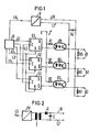
- FIG. 1 shows a data processing system D as a control unit. This outputs data via lines L1, L2 and L3 to the D inputs of three memory elements S1, S2 and S3 - each in the manner of a D flip-flop. The data are prompted in each case by a positive clock edge on a line L4 into the memory elements S1, S2 and S3.
- a logic “0” can be used to set each storage element S1, S2 or S3 to a basic position via a line L5.
- a identification signal is supplied to a converter U via a line L6.
- the converter U forms from this Identification signal a DC voltage.
- the input and the output of the converter U are electrically isolated from one another.
- the converter U exhibits "fail-safe" behavior, ie a failure of the identification signal leads to a voltage-free state at the output of the converter U.
- the positive potential of the output voltage from the converter U reaches the collector of phototransistors of the optocouplers 01 via line L7, 02 and 03.
- the emitters of these phototransistors lead to first poles of outputs A1, A2 and A3, which lead to processing devices which are not shown for the sake of clarity.
- the second pole of each of these outputs A1, A2 and A3 is given by the negative potential of the output voltage of the converter U. This potential is supplied via a line L8.
- a discharge resistor R4 is connected in parallel to the output of converter U, and a discharge resistor R5, R6 and R7 is connected in parallel to the output of each optocoupler 01, 02 and 03, respectively. If positive logic is assumed, due to the presence of a signal logic "1" at an input E, a positive voltage is constantly fed to the anode via a current-limiting series resistor R1, R2 and R3, in each case one of the luminance diodes assigned to one of the optocouplers 01, 02 or 03. The cathodes of these luminance diodes are each assigned to an inverting output of one of the memory elements S1, S2 or S3.
- the illustration according to FIG. 2 shows a special design of the converter U.
- the converter U receives the identification signal via the line L6, which is amplified in a switching amplifier SV.
- the power supply of the switching amplifier SV which also takes over the power supply of the data processing system D and the memory elements S1, S2 and S3, and supplies the input E with voltage, is not shown for the sake of clarity.
- the amplified identification signal, a clock signal reaches a primary winding of a transformer T, the secondary winding of which is galvanically separated from the primary winding.
- the transformed characteristic signal present at the secondary winding is rectified by an arrangement of a diode D and a capacitor C.
- the direct signal is forwarded via lines L7 and L8.
Landscapes
- Physics & Mathematics (AREA)
- Electromagnetism (AREA)
- Engineering & Computer Science (AREA)
- Computer Networks & Wireless Communication (AREA)
- Signal Processing (AREA)
- Analogue/Digital Conversion (AREA)
- Electronic Switches (AREA)
- Oscillators With Electromechanical Resonators (AREA)
- Semiconductor Integrated Circuits (AREA)
- Power Conversion In General (AREA)
- Cash Registers Or Receiving Machines (AREA)
- Safety Devices In Control Systems (AREA)
- Electric Propulsion And Braking For Vehicles (AREA)
- Dc-Dc Converters (AREA)
- Massaging Devices (AREA)
- Peptides Or Proteins (AREA)
- Electrotherapy Devices (AREA)
Priority Applications (1)
| Application Number | Priority Date | Filing Date | Title |
|---|---|---|---|
| AT83106800T ATE59241T1 (de) | 1982-07-21 | 1983-07-11 | Einrichtung zur potentialgetrennten signalausgabe bei einem steuerwerk. |
Applications Claiming Priority (2)
| Application Number | Priority Date | Filing Date | Title |
|---|---|---|---|
| DE19823227290 DE3227290A1 (de) | 1982-07-21 | 1982-07-21 | Einrichtung zur potentialgetrennten signalausgabe bei einem steuerwerk |
| DE3227290 | 1982-07-21 |
Publications (3)
| Publication Number | Publication Date |
|---|---|
| EP0101853A2 true EP0101853A2 (fr) | 1984-03-07 |
| EP0101853A3 EP0101853A3 (en) | 1987-10-14 |
| EP0101853B1 EP0101853B1 (fr) | 1990-12-19 |
Family
ID=6168976
Family Applications (1)
| Application Number | Title | Priority Date | Filing Date |
|---|---|---|---|
| EP83106800A Expired - Lifetime EP0101853B1 (fr) | 1982-07-21 | 1983-07-11 | Dispositif de délivrance de signaux à isolement galvanique pour un système de commande |
Country Status (4)
| Country | Link |
|---|---|
| EP (1) | EP0101853B1 (fr) |
| AT (1) | ATE59241T1 (fr) |
| DE (2) | DE3227290A1 (fr) |
| ZA (1) | ZA835268B (fr) |
Cited By (2)
| Publication number | Priority date | Publication date | Assignee | Title |
|---|---|---|---|---|
| EP0433965B1 (fr) * | 1989-12-21 | 1996-06-19 | Bosch-Siemens HausgerÀ¤te GmbH | Appareil électro-ménager ou pareil |
| EP0816746A1 (fr) * | 1996-06-28 | 1998-01-07 | Elan Schaltelemente GmbH | Dispositif d'interrupteur de sécurité |
Families Citing this family (1)
| Publication number | Priority date | Publication date | Assignee | Title |
|---|---|---|---|---|
| DK161227C (da) * | 1986-01-27 | 1991-11-25 | Antonson Security Denmark Aps | Apparat til synkronisering af tyveridetektorer |
Family Cites Families (3)
| Publication number | Priority date | Publication date | Assignee | Title |
|---|---|---|---|---|
| FR2222922A5 (en) * | 1973-03-22 | 1974-10-18 | Otic Fischer & Porter | Safety control system for explosive environments - using light waves to transmit control signals to hazardous area |
| CH594340A5 (en) * | 1975-07-10 | 1978-01-13 | Erni & Co Elektro Ind | Arrangement to isolate potentially interfering circuits |
| FR2381075A1 (fr) * | 1977-02-18 | 1978-09-15 | Lille Communaute Urbaine | Dispositif de commande de feux de circulation avec memoire |
-
1982
- 1982-07-21 DE DE19823227290 patent/DE3227290A1/de not_active Withdrawn
-
1983
- 1983-07-11 DE DE8383106800T patent/DE3382067D1/de not_active Expired - Lifetime
- 1983-07-11 EP EP83106800A patent/EP0101853B1/fr not_active Expired - Lifetime
- 1983-07-11 AT AT83106800T patent/ATE59241T1/de not_active IP Right Cessation
- 1983-07-20 ZA ZA835268A patent/ZA835268B/xx unknown
Cited By (2)
| Publication number | Priority date | Publication date | Assignee | Title |
|---|---|---|---|---|
| EP0433965B1 (fr) * | 1989-12-21 | 1996-06-19 | Bosch-Siemens HausgerÀ¤te GmbH | Appareil électro-ménager ou pareil |
| EP0816746A1 (fr) * | 1996-06-28 | 1998-01-07 | Elan Schaltelemente GmbH | Dispositif d'interrupteur de sécurité |
Also Published As
| Publication number | Publication date |
|---|---|
| EP0101853B1 (fr) | 1990-12-19 |
| EP0101853A3 (en) | 1987-10-14 |
| ATE59241T1 (de) | 1991-01-15 |
| DE3227290A1 (de) | 1984-01-26 |
| ZA835268B (en) | 1984-03-28 |
| DE3382067D1 (de) | 1991-01-31 |
Similar Documents
| Publication | Publication Date | Title |
|---|---|---|
| EP0033436B1 (fr) | Montage de traitement des informations composé de deux canaux dans le but d'assurer la sécurité des chemins de fer | |
| DE2458302A1 (de) | Netzteil mit einem sperrwandler fuer einen fernsehempfaenger mit ultraschallfernbedienung | |
| EP0268930A1 (fr) | Montage avec un commutateur de puissance autoprotégé | |
| DE2555603A1 (de) | Anordnung fuer positive sicherheit | |
| DE3112239A1 (de) | "schaltungsanordnung zur symmetrieregelung eines nach dem gegentaktprinzip arbeitenden gleichstromversorgungsgeraetes" | |
| CH634672A5 (de) | Digitale datenverarbeitungsanordnung, insbesondere fuer die eisenbahnsicherungstechnik. | |
| EP0101853B1 (fr) | Dispositif de délivrance de signaux à isolement galvanique pour un système de commande | |
| DE2806294A1 (de) | Einrichtung zur kontrolle des elektrischen leitungszustandes eines elektromechanischen schaltkontakts | |
| EP0198263A2 (fr) | Montage pour la transmission de signaux numériques sans mise à la terre par l'intermédiaire de points de séparation | |
| DE102019207968A1 (de) | Vorrichtung zur induktiven Übertragung elektrischer Energie | |
| DE2826897C2 (de) | Schaltungsanordnung zur erdfreien Übertragung von Signalen über Trennstellen in Fernmeldeanlagen | |
| EP0569883A2 (fr) | Constitution des circuits pour limitation du courant lors de la fermeture du circuit à ensemble électronique | |
| DE2555594A1 (de) | Anordnung zur steuerung mit positiver sicherheit | |
| DE3942427A1 (de) | Schaltungsanordnung zum aufbau unterbrechungsfreier stromversorgungseinheiten | |
| EP0292817A2 (fr) | Circuit pour l'obtention de signaux numériques bipolaires | |
| DE1073617B (de) | Schutzschaltung für Transistoren im Wechselrichterbetrieb | |
| DE2544427C2 (de) | Schaltungsanordnung zur Realisierung von logischen Funktionen | |
| DE2247276A1 (de) | Antivalenzkontrolleinrichtung fuer ein zweikanaliges schaltwerk | |
| DE3427221A1 (de) | Schaltungsanordnung fuer primaer getaktete schaltnetzteile | |
| DE2545469A1 (de) | Schaltungsanordnung zur logischen verknuepfung wechselspannungsfoermiger eingangssignale | |
| DE3330465A1 (de) | Spannungswandler | |
| DE2212832C3 (de) | Verfahren und Vorrichtung zur Überwachung und zum Schutz eines Parallelschwingkreiswechselrichters | |
| DE2900631B1 (de) | Sicherheits-Ausgabeschaltung | |
| DE2264360C3 (de) | Fehlersicherer Ausgabeverstärker | |
| AT334985B (de) | Schaltungsanordnung in fernmelde-, insbesondere fernsprechanlagen zur anschaltung einer signalwechselspannung an eine fernmelde-, insbesondere fernsprechleitung, oder an mehrere derartige leitungen |
Legal Events
| Date | Code | Title | Description |
|---|---|---|---|
| PUAI | Public reference made under article 153(3) epc to a published international application that has entered the european phase |
Free format text: ORIGINAL CODE: 0009012 |
|
| AK | Designated contracting states |
Designated state(s): AT CH DE FR GB LI NL SE |
|
| 17P | Request for examination filed |
Effective date: 19841119 |
|
| PUAL | Search report despatched |
Free format text: ORIGINAL CODE: 0009013 |
|
| AK | Designated contracting states |
Kind code of ref document: A3 Designated state(s): AT CH DE FR GB LI NL SE |
|
| 17Q | First examination report despatched |
Effective date: 19890331 |
|
| GRAA | (expected) grant |
Free format text: ORIGINAL CODE: 0009210 |
|
| AK | Designated contracting states |
Kind code of ref document: B1 Designated state(s): AT CH DE FR GB LI NL SE |
|
| REF | Corresponds to: |
Ref document number: 59241 Country of ref document: AT Date of ref document: 19910115 Kind code of ref document: T |
|
| REF | Corresponds to: |
Ref document number: 3382067 Country of ref document: DE Date of ref document: 19910131 |
|
| ET | Fr: translation filed | ||
| GBT | Gb: translation of ep patent filed (gb section 77(6)(a)/1977) | ||
| PLBE | No opposition filed within time limit |
Free format text: ORIGINAL CODE: 0009261 |
|
| STAA | Information on the status of an ep patent application or granted ep patent |
Free format text: STATUS: NO OPPOSITION FILED WITHIN TIME LIMIT |
|
| 26N | No opposition filed | ||
| EAL | Se: european patent in force in sweden |
Ref document number: 83106800.2 |
|
| PGFP | Annual fee paid to national office [announced via postgrant information from national office to epo] |
Ref country code: SE Payment date: 19970711 Year of fee payment: 15 |
|
| PGFP | Annual fee paid to national office [announced via postgrant information from national office to epo] |
Ref country code: NL Payment date: 19970714 Year of fee payment: 15 |
|
| PG25 | Lapsed in a contracting state [announced via postgrant information from national office to epo] |
Ref country code: SE Free format text: LAPSE BECAUSE OF NON-PAYMENT OF DUE FEES Effective date: 19980712 |
|
| PG25 | Lapsed in a contracting state [announced via postgrant information from national office to epo] |
Ref country code: NL Free format text: LAPSE BECAUSE OF NON-PAYMENT OF DUE FEES Effective date: 19990201 |
|
| EUG | Se: european patent has lapsed |
Ref document number: 83106800.2 |
|
| NLV4 | Nl: lapsed or anulled due to non-payment of the annual fee |
Effective date: 19990201 |
|
| PGFP | Annual fee paid to national office [announced via postgrant information from national office to epo] |
Ref country code: AT Payment date: 19990616 Year of fee payment: 17 |
|
| PGFP | Annual fee paid to national office [announced via postgrant information from national office to epo] |
Ref country code: GB Payment date: 19990709 Year of fee payment: 17 |
|
| PGFP | Annual fee paid to national office [announced via postgrant information from national office to epo] |
Ref country code: FR Payment date: 19990723 Year of fee payment: 17 |
|
| PGFP | Annual fee paid to national office [announced via postgrant information from national office to epo] |
Ref country code: DE Payment date: 19990917 Year of fee payment: 17 |
|
| PGFP | Annual fee paid to national office [announced via postgrant information from national office to epo] |
Ref country code: CH Payment date: 19991015 Year of fee payment: 17 |
|
| PG25 | Lapsed in a contracting state [announced via postgrant information from national office to epo] |
Ref country code: GB Free format text: LAPSE BECAUSE OF NON-PAYMENT OF DUE FEES Effective date: 20000711 Ref country code: AT Free format text: LAPSE BECAUSE OF NON-PAYMENT OF DUE FEES Effective date: 20000711 |
|
| PG25 | Lapsed in a contracting state [announced via postgrant information from national office to epo] |
Ref country code: LI Free format text: LAPSE BECAUSE OF NON-PAYMENT OF DUE FEES Effective date: 20000731 Ref country code: CH Free format text: LAPSE BECAUSE OF NON-PAYMENT OF DUE FEES Effective date: 20000731 |
|
| GBPC | Gb: european patent ceased through non-payment of renewal fee |
Effective date: 20000711 |
|
| REG | Reference to a national code |
Ref country code: CH Ref legal event code: PL |
|
| PG25 | Lapsed in a contracting state [announced via postgrant information from national office to epo] |
Ref country code: FR Free format text: LAPSE BECAUSE OF NON-PAYMENT OF DUE FEES Effective date: 20010330 |
|
| REG | Reference to a national code |
Ref country code: FR Ref legal event code: ST |
|
| PG25 | Lapsed in a contracting state [announced via postgrant information from national office to epo] |
Ref country code: DE Free format text: LAPSE BECAUSE OF NON-PAYMENT OF DUE FEES Effective date: 20010501 |