EP0101867A2 - Source d'ions à plasma - Google Patents
Source d'ions à plasma Download PDFInfo
- Publication number
- EP0101867A2 EP0101867A2 EP83106957A EP83106957A EP0101867A2 EP 0101867 A2 EP0101867 A2 EP 0101867A2 EP 83106957 A EP83106957 A EP 83106957A EP 83106957 A EP83106957 A EP 83106957A EP 0101867 A2 EP0101867 A2 EP 0101867A2
- Authority
- EP
- European Patent Office
- Prior art keywords
- electrode
- plasma
- disposed
- ion source
- deceleration
- Prior art date
- Legal status (The legal status is an assumption and is not a legal conclusion. Google has not performed a legal analysis and makes no representation as to the accuracy of the status listed.)
- Granted
Links
- 150000002500 ions Chemical class 0.000 claims abstract description 48
- 239000012212 insulator Substances 0.000 claims abstract description 32
- 230000001133 acceleration Effects 0.000 claims abstract description 28
- 238000000605 extraction Methods 0.000 claims abstract description 7
- 230000005684 electric field Effects 0.000 claims description 3
- 239000002245 particle Substances 0.000 description 11
- 238000010884 ion-beam technique Methods 0.000 description 10
- 229910001220 stainless steel Inorganic materials 0.000 description 4
- 239000010935 stainless steel Substances 0.000 description 4
- XYFCBTPGUUZFHI-UHFFFAOYSA-N Phosphine Chemical compound P XYFCBTPGUUZFHI-UHFFFAOYSA-N 0.000 description 3
- 238000010276 construction Methods 0.000 description 3
- RYGMFSIKBFXOCR-UHFFFAOYSA-N Copper Chemical compound [Cu] RYGMFSIKBFXOCR-UHFFFAOYSA-N 0.000 description 2
- 229910052802 copper Inorganic materials 0.000 description 2
- 239000010949 copper Substances 0.000 description 2
- 238000007789 sealing Methods 0.000 description 2
- 230000002195 synergetic effect Effects 0.000 description 2
- PNEYBMLMFCGWSK-UHFFFAOYSA-N Alumina Chemical compound [O-2].[O-2].[O-2].[Al+3].[Al+3] PNEYBMLMFCGWSK-UHFFFAOYSA-N 0.000 description 1
- -1 Phosphorus ions Chemical class 0.000 description 1
- 238000009792 diffusion process Methods 0.000 description 1
- 238000002474 experimental method Methods 0.000 description 1
- 238000009434 installation Methods 0.000 description 1
- 230000007246 mechanism Effects 0.000 description 1
- 230000005012 migration Effects 0.000 description 1
- 238000013508 migration Methods 0.000 description 1
- 229910052698 phosphorus Inorganic materials 0.000 description 1
- 239000011574 phosphorus Substances 0.000 description 1
- 229910000073 phosphorus hydride Inorganic materials 0.000 description 1
- 239000004065 semiconductor Substances 0.000 description 1
- 230000001960 triggered effect Effects 0.000 description 1
- 235000012431 wafers Nutrition 0.000 description 1
Images

Classifications
-
- H—ELECTRICITY
- H01—ELECTRIC ELEMENTS
- H01J—ELECTRIC DISCHARGE TUBES OR DISCHARGE LAMPS
- H01J27/00—Ion beam tubes
- H01J27/02—Ion sources; Ion guns
- H01J27/16—Ion sources; Ion guns using high-frequency excitation, e.g. microwave excitation
-
- H—ELECTRICITY
- H01—ELECTRIC ELEMENTS
- H01J—ELECTRIC DISCHARGE TUBES OR DISCHARGE LAMPS
- H01J27/00—Ion beam tubes
- H01J27/02—Ion sources; Ion guns
- H01J27/022—Details
Definitions
- the present invention relates to improvements in a plasma ion source in which an ion acceleration voltage for extracting ions from within a plasma is high, and more particularly to the structure of extraction lenses in the ion source of this type.
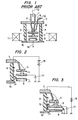
- FIG. 1 shows the sectional structure of the prior-art microwave plasma ion source.
- a microwave 13 generated by a microwave generator such as magnetron (not shovm) propagates along a circular or rectangular waveguide 1 and passes through a vacuum sealing dielectric plate 2, to be introduced into a discharge chamber 3 having a pair of confronting ridge electrodes (not shown).
- a feed gas such as phosphine (PH 3 ) is introduced into the discharge chamber 3 through a gas inlet pipe 9 by opening a needle valve 10.
- the feed gas introduced into the discharge chamber 3 discharges under the synergistic action of a microwave electric field formed across the aforementioned ridge electrodes and a magnetic field formed by a solenoid 11, so that a plasma is generated in the discharge chamber. 3.
- the discharge chamber 3 is usually held at a positive potential of several tens kV through an insulator 8, along with a flange ? and an acceleration electrode 4. From the plasma produced, ions are extracted through the slit of the acceleration electrode 4 disposed-in adjacency to the discharge chamber 3. The extracted ions advance toward a deceleration electrode 5 adjoining the acceleration electrode 4 and further pass through a grounded electrode 6 adjoining the deceleration electrode 5, to be extracted as an ion beam 14.
- the deceleration electrode 5 is usually held at a negative potential of several kV.
- Such microwave plasma ion source is used in an ion implanter for implanting ions into semiconductor wafers.
- the acceleration voltage to be applied to the acceleration electrode 4 was set at approximately 50 kV in order to increase the energy of the ion beam 14, there occurred the problem that a D.C. discharge of unknown cause began to arise across the deceleration electrode 5 and the grounded electrode 6, so the acceleration voltage 4 could not be supplied with a high voltage of at least 50 kV.
- This problem makes it impossible to cope with the requirements of ion implanters for increasingly higher acceleration voltages, and any countermeasure is desired.
- Such problem of discharge in an extraction electrode system arises, not only in the microwave plasma ion source as stated above, but also in other plasma ion sources in common.
- a plasma ion source is characterized by comprising a discharge chamber in which a plasma is produced by plasma generation means, an acceleration .electrode which is disposed in adjacency to said discharge chamber in order to extract ions from the produced plasma, a deceleration electrode which is disposed in adjacency to said acceleration electrode in order to decelerate the extracted ions, a ground electrode which is disposed in adjacency to said deceleration electrode, a container made of an insulator which is disposed so ' as to surround said discharge chamber and the respective electrodes, and a shield ring electrode of ground potential which is disposed in the vicinity of said deceleration electrode and along an inner wall surface of the insulator container in order to prevent any discharge from arising across said deceleration electrode and said ground electrode.
- the electric potential distribution of the inner wall surface of the insulator container 8 becomes quite different from that at the time at which the inner wall surface of the insulator container 8 is in a clean state.
- the high potential region of the flange 7 supplied with the high voltage by an acceleration voltage source 16 extends near to the grounded base 15. Then, the base 15 is bombarded with the ions by the surface creepage or by the migration of the charges in the vacuum, so that electrons e and ions ⁇ are emitted from the base 15.
- the emitted charged particles e and enter the space between the grounded electrode 6 and the deceleration electrode 5 which is supplied with a negative voltage by a deceleration voltage source 17. Therefore, the discharge takes place across the deceleration electrode 5 and the ground electrode 6 and generates a plasma. It is conjectured that the plasma will trigger the discharge on the acceleration electrode 4 and will make it impossible to apply the high voltage to the acceleration electrode 4.
- a shield ring electrode 12 may be disposed in the vicinity of the deceleration electrode 5 and along the inner wall surface of the insulator container 8. The shield ring electrode 12 is held in contact with the insulator container 8, or in close proximity to the insulator container 8.
- the shield ring electrode 12 is grounded.
- the provision of such shield ring electrode 12 makes it possible to reduce the charged particles e and attributed to the surface current flowing on the inner wall surface of the insulator container 8, and also to prevent the generated charged particles from entering the space between the deceleration electrode 5 and the ground electrode 6, so that the discharge across the deceleration electrode 5 and the ground electrode 6 can be perfectly prevented. It turns out that a high voltage of or above 50 kV can be applied to the acceleration electrode 4 and that an ion beam of high energy can - be extracted.
- FIG. 4 shows the sectional structure of a microwave plasma ion source according to the present invention.
- a microwave 13 which has been generated by a magnetron (not shotwn) having an output of 600 W and which has a frequency of 2.45 GHz propagates along a rectangular waveguide 1 made of copper and passes through a vacuum sealing dielectric plate 2 made of alumina ceramic, to be introduced into a discharge chamber 3 which is equipped with a pair of confronting ridge electrodes (not shown) made of copper.
- phosphine (PH 3 ) which is a feed gas is introduced into the discharge chamber 3 through a gas inlet pipe 9 by opening a needle valve 10.
- the PH 3 gas introduced into the discharge chamber 3 discharges under the synergistic action of a microwave electric field formed between the ridge electrodes and a D.C. magnetic field of about 1000 gausses formed by a solenoid 11.
- a plasma is formed within the discharge chamber 3.
- Phosphorus ions (P ) are extracted from the produced plasma through the slit of an acceleration electrode 4 of stainless steel which is disposed in adjacency to the discharge - chamber 3 and to which an acceleration voltage of +70 kV is applied.
- the extracted P ions advance toward a deceleration electrode 5 of stainless steel which is disposed in adjacency to the acceleration electrode 4 and to which a deceleration voltage of -2 kV is applied.
- a ground electrode 6 of stainless steel which is disposed in adjacency to the deceleration electrode 5 and which is grounded. Then, they are extracted .as a P + ion beam 14.
- a shield ring electrode 12 of stainless steel which forms the most important feature of the present invention is disposed in the vicinity of the deceleration electrode 5 and along the inner wall surface of the insulator container 8 in close proximity thereto. Moreover, the shield ring electrode 12 is grounded.
- the P + ion beam 14 of high energy could be stably extracted from such microwave plasma ion source over a long time, and the interelectrode discharge as in the prior art did not arise at all. Further, when the extraction of the P ion beam was conducted over a long time at an acceleration voltage raised to 80 kV, quite the no interelectrode discharge arose as in case of 70 kV, and a stable P + ion beam of high energy was obtained.
- Figure 5 shows the sectional structure of a shield ring electrode 12' in another plasma ion source according to the present invention.
- the shield ring electrode 12' is characterized in that the distance between its surface opposing to the insulator container 8 and the inner surface of the insulator container 8 increases gradually toward the acceleration electrode 4.
- a diffusion space for the charged particles generated by the bombardment of the shield ring electrode 12' with the charges having flowed along the inner wall surface of the insulator container 8 can be limited to a space defined by the insulator container a and the shield ring electrode 12', sc that the charged particles and e generated at this time can be prevented from widely diffusing into the other spaces.
- the charged particles and e can be more effectively prevented from entering the space between the deceleration electrcde 5 and the ground electrode 6.
- FIG. 6 shows the sectional structure of a shield ring electrode 12" in still another plasma ion source according to the present invention.
- the shield ring electrede 12" is characterized by having a ring-shaped spring 18 for contacting with the insulator container 8.
- the insulator container 8 is difficult to have a high dimensional accuracy because it is a sintered insulator. In ccnsequence, the distance between the shield ring electrode 12" and the insulator container 8 is prone to beccme ununiform depending upon places.
- the energy at which the surface of the shield ring electrode 12" is bombarded with the charges having flowed on the inner wall surface of the insulator container 8 becomes great, and an increased number of charged particles are generated at that time, so that the discharge across the electrodes is liable to be triggered. Therefore, the contact state between the shield ring electrode 12" and the insulator container 8 is improved by equipping the shield ring electrode 12" with the ring-shaped spring 18 as in the present embodiment.
- the functions of the shield ring electrode 12 are i) to reduce the charged particles which are generated when the charges flowing on the surface of the insulator container 8 bump into the base 15, and ii) to prevent the generated charged particles from entering the space between the deceleration electrode 5 and the ground electrode 6.
- the diametrical dimension of the shield ring electrode 12 be larger than the diameters. of the deceleration electrode 5 and the ground electrode 6.
- the top plane of the shield ring electrode 12 lie, at least, above the top plane of the ground electrcde 6.
- the * present invention has made it possible to raise an acceleration voltage to 80 kV from 50 kV in the prior art.
- a plasma ion source from which an ion beam of high energy can be extracted can be provided, and an ion implanter of high performance can be realized by employing such plasma ion source.
- microwave plasma ion source all While/the foregoing embodiments have referred to the microwave plasma ion source, it is needless to say that the present invention is not restricted to such plasma ion source but that it is similarly applicable to other plasma ion sources.
Landscapes
- Chemical & Material Sciences (AREA)
- Engineering & Computer Science (AREA)
- Combustion & Propulsion (AREA)
- Electron Sources, Ion Sources (AREA)
- Particle Accelerators (AREA)
Applications Claiming Priority (2)
| Application Number | Priority Date | Filing Date | Title |
|---|---|---|---|
| JP57131930A JPS5923432A (ja) | 1982-07-30 | 1982-07-30 | プラズマイオン源 |
| JP131930/82 | 1982-07-30 |
Publications (3)
| Publication Number | Publication Date |
|---|---|
| EP0101867A2 true EP0101867A2 (fr) | 1984-03-07 |
| EP0101867A3 EP0101867A3 (en) | 1985-08-14 |
| EP0101867B1 EP0101867B1 (fr) | 1988-01-13 |
Family
ID=15069527
Family Applications (1)
| Application Number | Title | Priority Date | Filing Date |
|---|---|---|---|
| EP83106957A Expired EP0101867B1 (fr) | 1982-07-30 | 1983-07-15 | Source d'ions à plasma |
Country Status (4)
| Country | Link |
|---|---|
| US (1) | US4629930A (fr) |
| EP (1) | EP0101867B1 (fr) |
| JP (1) | JPS5923432A (fr) |
| DE (1) | DE3375347D1 (fr) |
Cited By (4)
| Publication number | Priority date | Publication date | Assignee | Title |
|---|---|---|---|---|
| EP0135366A1 (fr) * | 1983-08-15 | 1985-03-27 | Applied Materials, Inc. | Système et procédé pour l'implantation d'ions |
| EP0154824A3 (en) * | 1984-03-16 | 1987-04-29 | Hitachi, Ltd. | Ion source |
| GB2261109B (en) * | 1991-10-04 | 1995-06-28 | Mitsubishi Electric Corp | Beam position monitor |
| GB2344931A (en) * | 1998-12-15 | 2000-06-21 | Hitachi Ltd | Ion beam processing apparatus and method of operating ion source therefor |
Families Citing this family (4)
| Publication number | Priority date | Publication date | Assignee | Title |
|---|---|---|---|---|
| US5053678A (en) * | 1988-03-16 | 1991-10-01 | Hitachi, Ltd. | Microwave ion source |
| US5206516A (en) * | 1991-04-29 | 1993-04-27 | International Business Machines Corporation | Low energy, steered ion beam deposition system having high current at low pressure |
| US5196706A (en) * | 1991-07-30 | 1993-03-23 | International Business Machines Corporation | Extractor and deceleration lens for ion beam deposition apparatus |
| US8674321B2 (en) * | 2012-02-28 | 2014-03-18 | Tiza Lab, L.L.C. | Microplasma ion source for focused ion beam applications |
Family Cites Families (7)
| Publication number | Priority date | Publication date | Assignee | Title |
|---|---|---|---|---|
| US3814975A (en) * | 1969-08-06 | 1974-06-04 | Gen Electric | Electron emission system |
| US3767952A (en) * | 1972-10-24 | 1973-10-23 | Ca Atomic Energy Ltd | Ion source with reduced emittance |
| DE2610165C2 (de) * | 1976-03-11 | 1983-11-10 | Gesellschaft für Schwerionenforschung mbH, 6100 Darmstadt | Duoplasmatron-Ionenquelle zur Erzeugung mehrfach geladener Ionen |
| US4058748A (en) * | 1976-05-13 | 1977-11-15 | Hitachi, Ltd. | Microwave discharge ion source |
| JPS5593644A (en) * | 1979-01-08 | 1980-07-16 | Nippon Telegr & Teleph Corp <Ntt> | Method of yielding ion using ion source device |
| JPS5947421B2 (ja) * | 1980-03-24 | 1984-11-19 | 株式会社日立製作所 | マイクロ波イオン源 |
| JPS57132632A (en) * | 1981-02-09 | 1982-08-17 | Hitachi Ltd | Ion source |
-
1982
- 1982-07-30 JP JP57131930A patent/JPS5923432A/ja active Pending
-
1983
- 1983-07-15 DE DE8383106957T patent/DE3375347D1/de not_active Expired
- 1983-07-15 EP EP83106957A patent/EP0101867B1/fr not_active Expired
- 1983-07-27 US US06/517,696 patent/US4629930A/en not_active Expired - Lifetime
Cited By (7)
| Publication number | Priority date | Publication date | Assignee | Title |
|---|---|---|---|---|
| EP0135366A1 (fr) * | 1983-08-15 | 1985-03-27 | Applied Materials, Inc. | Système et procédé pour l'implantation d'ions |
| EP0154824A3 (en) * | 1984-03-16 | 1987-04-29 | Hitachi, Ltd. | Ion source |
| GB2261109B (en) * | 1991-10-04 | 1995-06-28 | Mitsubishi Electric Corp | Beam position monitor |
| US5459393A (en) * | 1991-10-04 | 1995-10-17 | Mitsubishi Denki Kabushiki Kaisha | Beam position monitor and beam position detecting method |
| GB2344931A (en) * | 1998-12-15 | 2000-06-21 | Hitachi Ltd | Ion beam processing apparatus and method of operating ion source therefor |
| US6515426B1 (en) | 1998-12-15 | 2003-02-04 | Hitachi, Ltd. | Ion beam processing apparatus and method of operating ion source therefor |
| US6635998B2 (en) | 1998-12-15 | 2003-10-21 | Hitachi, Ltd. | Ion beam processing apparatus and method of operating ion source therefor |
Also Published As
| Publication number | Publication date |
|---|---|
| JPS5923432A (ja) | 1984-02-06 |
| DE3375347D1 (en) | 1988-02-18 |
| EP0101867B1 (fr) | 1988-01-13 |
| EP0101867A3 (en) | 1985-08-14 |
| US4629930A (en) | 1986-12-16 |
Similar Documents
| Publication | Publication Date | Title |
|---|---|---|
| US5576538A (en) | Apparatus and method for ion beam neutralization | |
| KR102478896B1 (ko) | 이온-이온 플라즈마 원자 층 에칭 프로세스 및 반응기 | |
| US4857809A (en) | Microwave ion source | |
| US6237527B1 (en) | System for improving energy purity and implant consistency, and for minimizing charge accumulation of an implanted substrate | |
| US7176469B2 (en) | Negative ion source with external RF antenna | |
| US6528805B2 (en) | Dose monitor for plasma doping system | |
| US5365070A (en) | Negative ion beam injection apparatus with magnetic shield and electron removal means | |
| US10068758B2 (en) | Ion mass separation using RF extraction | |
| US5032205A (en) | Plasma etching apparatus with surface magnetic fields | |
| US4316090A (en) | Microwave plasma ion source | |
| US5750987A (en) | Ion beam processing apparatus | |
| US8796649B2 (en) | Ion implanter | |
| EP0101867B1 (fr) | Source d'ions à plasma | |
| US4749910A (en) | Electron beam-excited ion beam source | |
| JPH05106037A (ja) | イオン注入装置及びその制御方法 | |
| US9721760B2 (en) | Electron beam plasma source with reduced metal contamination | |
| EP0685872A1 (fr) | Implanteur ionique | |
| US5545257A (en) | Magnetic filter apparatus and method for generating cold plasma in semicoductor processing | |
| TW202338884A (zh) | 環狀運動加強型離子源 | |
| US12518946B2 (en) | Integrated gas box and ion source | |
| JPH0325846A (ja) | イオンビーム照射装置における電荷中和装置 | |
| US12597588B2 (en) | Inductively coupled plasma apparatus with novel faraday shield | |
| US20240412899A1 (en) | Self-centering voltage standoff | |
| EP0095879B1 (fr) | Equipement et méthode pour le traitement des surfaces avec un faisceau d'ions à basse énergie et haute intensité | |
| JPS62108428A (ja) | イオン源 |
Legal Events
| Date | Code | Title | Description |
|---|---|---|---|
| PUAI | Public reference made under article 153(3) epc to a published international application that has entered the european phase |
Free format text: ORIGINAL CODE: 0009012 |
|
| 17P | Request for examination filed |
Effective date: 19830715 |
|
| AK | Designated contracting states |
Designated state(s): DE FR GB NL |
|
| PUAL | Search report despatched |
Free format text: ORIGINAL CODE: 0009013 |
|
| AK | Designated contracting states |
Designated state(s): DE FR GB NL |
|
| 17Q | First examination report despatched |
Effective date: 19870520 |
|
| GRAA | (expected) grant |
Free format text: ORIGINAL CODE: 0009210 |
|
| AK | Designated contracting states |
Kind code of ref document: B1 Designated state(s): DE FR GB |
|
| REF | Corresponds to: |
Ref document number: 3375347 Country of ref document: DE Date of ref document: 19880218 |
|
| ET | Fr: translation filed | ||
| PLBE | No opposition filed within time limit |
Free format text: ORIGINAL CODE: 0009261 |
|
| STAA | Information on the status of an ep patent application or granted ep patent |
Free format text: STATUS: NO OPPOSITION FILED WITHIN TIME LIMIT |
|
| 26N | No opposition filed | ||
| REG | Reference to a national code |
Ref country code: GB Ref legal event code: IF02 |
|
| PGFP | Annual fee paid to national office [announced via postgrant information from national office to epo] |
Ref country code: FR Payment date: 20020619 Year of fee payment: 20 |
|
| PGFP | Annual fee paid to national office [announced via postgrant information from national office to epo] |
Ref country code: GB Payment date: 20020621 Year of fee payment: 20 |
|
| PGFP | Annual fee paid to national office [announced via postgrant information from national office to epo] |
Ref country code: DE Payment date: 20020916 Year of fee payment: 20 |
|
| PG25 | Lapsed in a contracting state [announced via postgrant information from national office to epo] |
Ref country code: GB Free format text: LAPSE BECAUSE OF EXPIRATION OF PROTECTION Effective date: 20030714 |
|
| REG | Reference to a national code |
Ref country code: GB Ref legal event code: PE20 |