EP0102075B1 - Dispositif semi-conducteur avec une structure à multicouches - Google Patents
Dispositif semi-conducteur avec une structure à multicouches Download PDFInfo
- Publication number
- EP0102075B1 EP0102075B1 EP83108445A EP83108445A EP0102075B1 EP 0102075 B1 EP0102075 B1 EP 0102075B1 EP 83108445 A EP83108445 A EP 83108445A EP 83108445 A EP83108445 A EP 83108445A EP 0102075 B1 EP0102075 B1 EP 0102075B1
- Authority
- EP
- European Patent Office
- Prior art keywords
- region
- mesa
- conductivity type
- layer
- film
- Prior art date
- Legal status (The legal status is an assumption and is not a legal conclusion. Google has not performed a legal analysis and makes no representation as to the accuracy of the status listed.)
- Expired
Links
Images



Classifications
-
- H—ELECTRICITY
- H10—SEMICONDUCTOR DEVICES; ELECTRIC SOLID-STATE DEVICES NOT OTHERWISE PROVIDED FOR
- H10D—INORGANIC ELECTRIC SEMICONDUCTOR DEVICES
- H10D48/00—Individual devices not covered by groups H10D1/00 - H10D44/00
- H10D48/30—Devices controlled by electric currents or voltages
- H10D48/32—Devices controlled by only the electric current supplied, or only the electric potential applied, to an electrode which does not carry the current to be rectified, amplified or switched
- H10D48/34—Bipolar devices
- H10D48/345—Bipolar transistors having ohmic electrodes on emitter-like, base-like, and collector-like regions
-
- H—ELECTRICITY
- H10—SEMICONDUCTOR DEVICES; ELECTRIC SOLID-STATE DEVICES NOT OTHERWISE PROVIDED FOR
- H10W—GENERIC PACKAGES, INTERCONNECTIONS, CONNECTORS OR OTHER CONSTRUCTIONAL DETAILS OF DEVICES COVERED BY CLASS H10
- H10W20/00—Interconnections in chips, wafers or substrates
- H10W20/40—Interconnections external to wafers or substrates, e.g. back-end-of-line [BEOL] metallisations or vias connecting to gate electrodes
Definitions
- This invention relates to a semiconductor device, and more particularly to a semiconductor device including a bipolar transistor.
- the switching speed and power dissipation of a semiconductor device which are the basic standards for indicating its performance, are determined by the value of the current in the transistor employed therein, and by the electrostatic capacitance of the elements, including parasitic elements, whose charge and discharge must be made with this current. It is desirable that the value of this capacitance is as small as possible, because the power required to operate the transistor is proportional to the capacitance for a given current. In addition, the capacitance must be reduced in order to increase the switching speed of the transistor, because the RC time constant of the transistor is proportional to the capacitance for a given sheet resistance.
- Some of the present inventors have developed a semiconductor device including a bipolar transistor, etc., whose power dissipation is small, which operates at a high speed, and wherein the elements occupy a small area, by isolating the active region, etc., of the semiconductor from the substrate thereof by an insulation film, thereby reducing a parasitic capacitance, and they have already filed a patent application therefor (EP-A-0078501 ).
- Figure 1 is a section through the structure of one example of this semiconductor device.
- the following is a description thereof, the material of each part and the conductivity types of the semiconductor layers are prescribed (the first conductivity type is taken to be n-type and the second conductivity type to be p-type) therein so as to simplify the explanation.
- This also applies to the description of the present invention below, needless to say the materials and conductivity types are not limited thereto.
- numeral 1 denotes an Si substrate of p-type conductivity, 2 a buried layer of n +- type conductivity, and 3, 4 and 5 epitaxially-grown Si layers of which 3 is an n-type conductivity region, 4 a p-type conductivity region, and 5 and n +- type conductivity region. Each of these regions is formed by the doping of impurities.
- Numeral 6 denotes an insulation film, 7 a polycrystalline semiconductor layer, 8 an insulation film, and 9 an electrode.
- Numeral (I) denotes a lateral bipolar transistor wherein the electrodes of the emitter and collector regions 4-1 and 4-2 are taken out through the polycrystalline semiconductor layer 7 between the insulation films 6 and 8.
- Numeral (II) denotes a vertical bipolar transistor wherein the electrodes of base regions (an intrinsic base region 4-3 and a graft base region 4-4) are also taken out through the polycrystalline semiconductor layer 7 between the insulation films 6 and 8.
- the structure of the transistors shown in Figure 1 has the advantages that it enables high-speed operation because of their small parasitic capacitance, and that it also enables a reduction of the area of the elements.
- the resistance thereof is not reduced, since the take-out electrodes from the active region formed of a monocrystalline layer are constituted by the polycrystalline semiconductor layer 7.
- the time constant expressed as the product of the resistance and the capacitance, is reduced only by the effect of the reduction of the parasitic capacitance, the realization of high-speed operation is hindered in a circuit wherein a number of multi-emitter structures are used, since the speed of operation is determined by the time constant of the slowest emitter. This is because the time constant of each emitter is affected by the resistance of the polycrystalline semiconductor layer.
- Monocrystalline p-type conductivity regions 4 (4-1, 4-2 and 4-4) in contact with the polycrystalline semiconductor layer 7 are formed by the diffusion of the p-type impurities from the polycrystalline semiconductor layer 7. That is, the p-type graft base region 4-4 is formed by diffusion from an unstable polycrystalline semiconductor region with a different diffusion constant, due to differences in the process conditions. This makes it difficult to control the depth of the graft base, and thus it has been difficult to manufacture an element with an emitter (n +- type region 5) of a small area.
- US-A-4,338,138 discloses a semiconductor device which is similar in the relevant respects to the structure shown in Figure 1. The first part of claim 1 has been drafted in view of this prior art.
- the invention meets this object by the features characterized in claim 1.
- the metal silicide region provided on the polycrystalline silicon layer results in a reduction of the resistivity which, in turn, enables a high-speed, low-power operation of the device.
- FIG. 2 is a section through the structure of a first embodiment of the semiconductor of the present invention.
- electrodes 18, 19 takens out from monocrystalline regions form a double-layer structure to reduce the resistance thereof.
- the electrodes 18 and 19 have a double-layer structure formed, for instance, of a polycrystalline semiconductor (a polycrystalline silicon layer) as one layer, and a metal silicide as the other.
- Electrodes 18 and 19 taken out from base regions (4-3 and 4-4) are isolated from an emitter region (n +- type region 5) by an oxide film (insulation film 8), the base and emitter regions can also be formed by a self-alignment method.
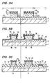
- Figures 3A to 3F illustrate the process of manufacturing the semiconductor device shown in Fig.
- n +- type buried layer 2 is formed in a p-type Si substrate 1 by diffusion of impurities, an n-type Si layer 11 is grown epitaxially thereon, a silicon oxide film 12, a silicon nitride film (Si 3 N 4 ) 13, and another silicon oxide film 14 are formed over the whole surface in that order, and then these three layers are removed by etching except for the parts that will form the active regions of the transistors.
- the epitaxial layer 11 is also etched, as shown in the figure, to form mesa regions (3).
- a silicon oxide film 15 is formed by the thermal oxidation.
- a silicon nitride film 16 and a silicon oxide film 17 are then deposited in that order, and the oxide film 17 is etched so that it remains only in the region wherein the collector electrode of the longitudinal transistor will be formed.
- the nitride film 16 is then etched by reactive sputter etching so that it is left only on the sidewalls of the mesa regions 3, and in the region wherein the collector electrode will be formed.
- An oxide film 6 is formed by thermal oxidation, nitride film 16 and the oxide film 15 are removed, and a p-type region 4 is formed by the thermal diffusion of impurities.
- a polycrystalline silicon film 18 and a film 19 of a refractory metal or a metal silicide are deposited.
- a refractory metal or a metal silicide e.g a molybdenum silicide, tungsten silicide, palladium silicide, nickel silicide, etc.,
- the film 19 is formed of a refractory metal, it is made into the silicide together with the polycrystalline silicon film 18, and is formed into one body therewith, by annealing later.
- the polycrystalline silicon film 18 is lightly doped to be p-type.
- a photoresist film (e.g. KTFR of Kodak Company) 20 is applied, and the areas covering the mesa regions are etched so that they are slightly broader than the mesas.
- a coating of a photoresist (e.g. AZ1350J of Hexit Co., Ltd. or Microposit 1300 of Shipley Co., Ltd.) 21 is then applied so that it penetrates the spaces between the mesa regions (the mesas of the Si epitaxial layer 11) and the photoresist film 20, and also covers their upper surfaces. Therefore these surfaces are flat after the coating.
- the photoresist is etched in an O2 atmosphere, the etching is stopped when the metal silicide film 19 on the mesa regions is exposed.
- the layers of the metal silicide film 19 and the polycrystalline silicon film 18 are then removed by a plasma etching method in such a way that only the metal silicide film 19 and the polycrystalline silicon film 18 located on the top surfaces of the mesa regions are removed, so that the silicon oxide film 14 is exposed.
- a passivation silicon nitride film 22 is deposited, a hole is made which will form the emitter region, emitter impurities are added, and thereby the emitter region (n + region 5) is formed. After that, an electrode 9 for each region is formed.
- the semiconductor device of the present invention is formed by the above process.
- the graft base region 4-4 in the semiconductor device of the present invention can be formed very accurately, since it is not formed by the diffusion of impurities from the polycrystalline silicon film 18.
- high-speed operation is enabled, since electrodes taken out from an active region formed by monocrystalline layers have a two- layer structure of a polycrystalline silicon film 18 and a metal silicide film 19 which enables a reduction of the resistance.
- Figures 4A to 4D illustrate the process of.manufacturing a second embodiment of the semiconductor device of the present invention.
- Figure 4D is a section through the structure of a completed semiconductor device of the present invention.
- the polycrystalline silicon film 18 is deposited and doped slightly to be p-type. Next, only the polycrystalline silicon on the mesa regions is removed in the same way as in the first embodiment, and then the polycrystalline silicon film 18 is etched by a conventional photoetching process. After that, the oxide film 14 is etched, and then the film 19 of a refractory metal such as tungsten, molybdenum, palladium, nickel, etc., is deposited.
- a refractory metal such as tungsten, molybdenum, palladium, nickel, etc.
- the polycrystalline silicon film 18 and the refractory metal film 19 are made to react with each other by annealing, so that a layer 23 of metal silicide is formed only on the polycrystalline silicon film 18 and the regions around it.
- the annealing temperature depends upon the kind of refractory metal, the deposition method, and the annealing gas.
- the refractory metal film 19 is formed of tungsten deposited by a sputtering method and the annealing gas is hydrogen, for instance, an annealing temperature of between 600°C to 900°C is suitable.
- the annealing temperature is less than 600°C, the growth rate of the metal silicide is very low, and when it is more than 900°C, the growth rate of the metal silicide layer 23 is extremely high, which results in the formation of the metal silicide layer 23 even in regions some distance from the polycrystalline silicon film 18. This could cause short- circuits, via the metal silicide, between the parts of the pattern of the polycrystalline silicon film 18.
- the annealing conditions are set so that some of the metal silicide layer also grows in the peripheral regions around the polycrystalline silicon film 18. This means that the metal silicide layer 23 is formed around the periphery of the silicon nitride film 13 on the mesa regions (3).
- the refractory metal film 19 is removed by etching (the un-reacted refractory metal film can be left as it is on the metal silicide layer 23), and a silicon oxide film 24 is formed over the metal silicide layer 23 by a oxidation process or a deposition method.
- the silicon nitride film 13 is then removed by using the oxide film 24 as a mask, and the base region 4-3 is formed by a conventional ion implantation method.
- the collector electrode regions of the lateral transistor region (I) and the longitudinal transistor region (11) are covered with a photoresist to prevent the implantation of ions therein.
- the emitter region (n +- type region 5) is formed thereafter by ion implantation, and the silicon nitride film 25 and the oxide films 24 and 12 are etched by a conventional photoetching process to form a base contact hole 26 and a collector contact hole 27, and electrodes 9 are then formed.
- the layers of the polycrystalline silicon film 18 for the base electrodes and the metal silicide film 23 are isolated from the emitter region 5 by the oxide film 24 and the silicon nitride film 13, and thus the base electrodes and the emitter region can be formed so as to be self-aligning.
- the base electrodes are also isolated from the emitter region in a self-aligning manner in the first embodiment, they are isolated from each other in .that embodiment by the oxide grown below the silicon nitride film 13. This oxide grown below the silicon nitride film is a called a bird beak. Its growth depends upon the oxidation conditions, the thickness of the silicon oxide film 12, the thickness of the silicon nitride film 13, etc., and it is somewhat inferior to that in the second embodiment in terms of the control of the quantity of growth.
- the propagation delay time (tp d min ) of the element of the conventional method is 2500 ps, while that of the element according to the present invention is 500 ps.
- This large improvement makes it possible to manufacture a PLA (Programmable Logic Array) formed of 1 2 Ls with at least four collectors, which has been impossible so far.
Landscapes
- Bipolar Transistors (AREA)
Claims (12)
Applications Claiming Priority (2)
| Application Number | Priority Date | Filing Date | Title |
|---|---|---|---|
| JP57149227A JPS5940571A (ja) | 1982-08-30 | 1982-08-30 | 半導体装置 |
| JP149227/82 | 1982-08-30 |
Publications (3)
| Publication Number | Publication Date |
|---|---|
| EP0102075A2 EP0102075A2 (fr) | 1984-03-07 |
| EP0102075A3 EP0102075A3 (en) | 1986-02-05 |
| EP0102075B1 true EP0102075B1 (fr) | 1990-03-21 |
Family
ID=15470640
Family Applications (1)
| Application Number | Title | Priority Date | Filing Date |
|---|---|---|---|
| EP83108445A Expired EP0102075B1 (fr) | 1982-08-30 | 1983-08-26 | Dispositif semi-conducteur avec une structure à multicouches |
Country Status (5)
| Country | Link |
|---|---|
| EP (1) | EP0102075B1 (fr) |
| JP (1) | JPS5940571A (fr) |
| KR (1) | KR900008149B1 (fr) |
| CA (1) | CA1205577A (fr) |
| DE (1) | DE3381366D1 (fr) |
Families Citing this family (5)
| Publication number | Priority date | Publication date | Assignee | Title |
|---|---|---|---|---|
| JPS6170757A (ja) * | 1984-09-14 | 1986-04-11 | Hitachi Ltd | 半導体装置及びその製造方法 |
| JPS61164262A (ja) * | 1985-01-17 | 1986-07-24 | Toshiba Corp | 半導体装置 |
| JPS61166071A (ja) * | 1985-01-17 | 1986-07-26 | Toshiba Corp | 半導体装置及びその製造方法 |
| US5397912A (en) * | 1991-12-02 | 1995-03-14 | Motorola, Inc. | Lateral bipolar transistor |
| US6140694A (en) * | 1998-12-30 | 2000-10-31 | Philips Electronics North America Corporation | Field isolated integrated injection logic gate |
Family Cites Families (5)
| Publication number | Priority date | Publication date | Assignee | Title |
|---|---|---|---|---|
| US4338138A (en) * | 1980-03-03 | 1982-07-06 | International Business Machines Corporation | Process for fabricating a bipolar transistor |
| US4259680A (en) * | 1980-04-17 | 1981-03-31 | Bell Telephone Laboratories, Incorporated | High speed lateral bipolar transistor |
| US4339767A (en) * | 1980-05-05 | 1982-07-13 | International Business Machines Corporation | High performance PNP and NPN transistor structure |
| US4403394A (en) * | 1980-12-17 | 1983-09-13 | International Business Machines Corporation | Formation of bit lines for ram device |
| JPS5873156A (ja) * | 1981-10-28 | 1983-05-02 | Hitachi Ltd | 半導体装置 |
-
1982
- 1982-08-30 JP JP57149227A patent/JPS5940571A/ja active Pending
-
1983
- 1983-07-29 CA CA000433567A patent/CA1205577A/fr not_active Expired
- 1983-08-05 KR KR1019830003667A patent/KR900008149B1/ko not_active Expired
- 1983-08-26 DE DE8383108445T patent/DE3381366D1/de not_active Expired - Lifetime
- 1983-08-26 EP EP83108445A patent/EP0102075B1/fr not_active Expired
Also Published As
| Publication number | Publication date |
|---|---|
| EP0102075A3 (en) | 1986-02-05 |
| DE3381366D1 (de) | 1990-04-26 |
| CA1205577A (fr) | 1986-06-03 |
| EP0102075A2 (fr) | 1984-03-07 |
| JPS5940571A (ja) | 1984-03-06 |
| KR840005930A (ko) | 1984-11-19 |
| KR900008149B1 (ko) | 1990-11-03 |
Similar Documents
| Publication | Publication Date | Title |
|---|---|---|
| US4481706A (en) | Process for manufacturing integrated bi-polar transistors of very small dimensions | |
| US4252582A (en) | Self aligned method for making bipolar transistor having minimum base to emitter contact spacing | |
| US4691435A (en) | Method for making Schottky diode having limited area self-aligned guard ring | |
| EP0170250B1 (fr) | Transistor bipolaire et son procédé de fabrication | |
| US5070030A (en) | Method of making an oxide isolated, lateral bipolar transistor | |
| US5187109A (en) | Lateral bipolar transistor and method of making the same | |
| US4301588A (en) | Consumable amorphous or polysilicon emitter process | |
| US4029522A (en) | Method to fabricate ion-implanted layers with abrupt edges to reduce the parasitic resistance of Schottky barrier fets and bipolar transistors | |
| EP0160255B1 (fr) | Dispositif à transistor à effet de champ et son procédé de fabrication | |
| US4545113A (en) | Process for fabricating a lateral transistor having self-aligned base and base contact | |
| JPH0630359B2 (ja) | バイポーラトランジスタの製造方法 | |
| EP0051534B1 (fr) | Procédé de fabrication auto-alignée de structures de circuits intégrés employant différents taux de croissance de l'oxyde | |
| EP0052038B1 (fr) | Procédé de fabrication d'une structure de circuit integré | |
| US4860086A (en) | Semiconductor device | |
| US4792837A (en) | Orthogonal bipolar transistor | |
| EP0159179A2 (fr) | Construction d'un transistor bipolaire | |
| EP0102075A2 (fr) | Dispositif semi-conducteur avec une structure à multicouches | |
| US4713355A (en) | Bipolar transistor construction | |
| US4352238A (en) | Process for fabricating a vertical static induction device | |
| EP0034341B1 (fr) | Procédé de fabrication d'un dispositif semiconducteur | |
| KR880000483B1 (ko) | 반도체소자의 제조방법 | |
| EP0036499A1 (fr) | Procédé auto-aligné pour transistor bipolaire à base en polysilicium | |
| US4449284A (en) | Method of manufacturing an integrated circuit device having vertical field effect transistors | |
| US20040209433A1 (en) | Method for manufacturing and structure of semiconductor device with shallow trench collector contact region | |
| EP0042380B1 (fr) | Procédé permettant d'obtenir un profil de concentration d'impuretés ideal dans la base d'un transistor |
Legal Events
| Date | Code | Title | Description |
|---|---|---|---|
| PUAI | Public reference made under article 153(3) epc to a published international application that has entered the european phase |
Free format text: ORIGINAL CODE: 0009012 |
|
| AK | Designated contracting states |
Designated state(s): DE FR GB IT NL |
|
| 17P | Request for examination filed |
Effective date: 19841220 |
|
| PUAL | Search report despatched |
Free format text: ORIGINAL CODE: 0009013 |
|
| AK | Designated contracting states |
Designated state(s): DE FR GB IT NL |
|
| 17Q | First examination report despatched |
Effective date: 19880125 |
|
| GRAA | (expected) grant |
Free format text: ORIGINAL CODE: 0009210 |
|
| AK | Designated contracting states |
Kind code of ref document: B1 Designated state(s): DE FR GB IT NL |
|
| PG25 | Lapsed in a contracting state [announced via postgrant information from national office to epo] |
Ref country code: NL Effective date: 19900321 Ref country code: IT Free format text: LAPSE BECAUSE OF FAILURE TO SUBMIT A TRANSLATION OF THE DESCRIPTION OR TO PAY THE FEE WITHIN THE PRESCRIBED TIME-LIMIT;WARNING: LAPSES OF ITALIAN PATENTS WITH EFFECTIVE DATE BEFORE 2007 MAY HAVE OCCURRED AT ANY TIME BEFORE 2007. THE CORRECT EFFECTIVE DATE MAY BE DIFFERENT FROM THE ONE RECORDED. Effective date: 19900321 |
|
| REF | Corresponds to: |
Ref document number: 3381366 Country of ref document: DE Date of ref document: 19900426 |
|
| ET | Fr: translation filed | ||
| NLV1 | Nl: lapsed or annulled due to failure to fulfill the requirements of art. 29p and 29m of the patents act | ||
| PLBE | No opposition filed within time limit |
Free format text: ORIGINAL CODE: 0009261 |
|
| STAA | Information on the status of an ep patent application or granted ep patent |
Free format text: STATUS: NO OPPOSITION FILED WITHIN TIME LIMIT |
|
| 26N | No opposition filed | ||
| PGFP | Annual fee paid to national office [announced via postgrant information from national office to epo] |
Ref country code: GB Payment date: 19950816 Year of fee payment: 13 |
|
| PGFP | Annual fee paid to national office [announced via postgrant information from national office to epo] |
Ref country code: FR Payment date: 19950817 Year of fee payment: 13 |
|
| PGFP | Annual fee paid to national office [announced via postgrant information from national office to epo] |
Ref country code: DE Payment date: 19951026 Year of fee payment: 13 |
|
| PG25 | Lapsed in a contracting state [announced via postgrant information from national office to epo] |
Ref country code: GB Effective date: 19960826 |
|
| GBPC | Gb: european patent ceased through non-payment of renewal fee |
Effective date: 19960826 |
|
| PG25 | Lapsed in a contracting state [announced via postgrant information from national office to epo] |
Ref country code: FR Effective date: 19970430 |
|
| PG25 | Lapsed in a contracting state [announced via postgrant information from national office to epo] |
Ref country code: DE Effective date: 19970501 |
|
| REG | Reference to a national code |
Ref country code: FR Ref legal event code: ST |