EP0102174B1 - Perfectionnements aux amplificateurs de transimpédance ou y relatifs - Google Patents
Perfectionnements aux amplificateurs de transimpédance ou y relatifs Download PDFInfo
- Publication number
- EP0102174B1 EP0102174B1 EP83304205A EP83304205A EP0102174B1 EP 0102174 B1 EP0102174 B1 EP 0102174B1 EP 83304205 A EP83304205 A EP 83304205A EP 83304205 A EP83304205 A EP 83304205A EP 0102174 B1 EP0102174 B1 EP 0102174B1
- Authority
- EP
- European Patent Office
- Prior art keywords
- amplifier
- component
- input
- impedance
- current
- Prior art date
- Legal status (The legal status is an assumption and is not a legal conclusion. Google has not performed a legal analysis and makes no representation as to the accuracy of the status listed.)
- Expired
Links
Images
Classifications
-
- H—ELECTRICITY
- H03—ELECTRONIC CIRCUITRY
- H03G—CONTROL OF AMPLIFICATION
- H03G3/00—Gain control in amplifiers or frequency changers
- H03G3/20—Automatic control
- H03G3/30—Automatic control in amplifiers having semiconductor devices
- H03G3/3084—Automatic control in amplifiers having semiconductor devices in receivers or transmitters for electromagnetic waves other than radiowaves, e.g. lightwaves
-
- H—ELECTRICITY
- H03—ELECTRONIC CIRCUITRY
- H03F—AMPLIFIERS
- H03F3/00—Amplifiers with only discharge tubes or only semiconductor devices as amplifying elements
- H03F3/04—Amplifiers with only discharge tubes or only semiconductor devices as amplifying elements with semiconductor devices only
- H03F3/08—Amplifiers with only discharge tubes or only semiconductor devices as amplifying elements with semiconductor devices only controlled by light
- H03F3/087—Amplifiers with only discharge tubes or only semiconductor devices as amplifying elements with semiconductor devices only controlled by light with IC amplifier blocks
-
- H—ELECTRICITY
- H04—ELECTRIC COMMUNICATION TECHNIQUE
- H04B—TRANSMISSION
- H04B10/00—Transmission systems employing electromagnetic waves other than radio-waves, e.g. infrared, visible or ultraviolet light, or employing corpuscular radiation, e.g. quantum communication
- H04B10/60—Receivers
- H04B10/66—Non-coherent receivers, e.g. using direct detection
- H04B10/69—Electrical arrangements in the receiver
- H04B10/691—Arrangements for optimizing the photodetector in the receiver
Definitions
- This invention relates to transimpedance amplifiers for use in optical receivers.
- Optical receivers are an integral part of light guide systems utilized for optical communication. Optical receivers generally have a limited dynamic range which in this instance is defined as the range of optical power between the minimum allowable level for a given system margin and the maximum level before overloading occurs. If the transmitters and receivers are to be located at fixed distances from each other, a translucent attenuator is often placed within the optical fibre at a certain point in the transmission segment such that the received signal is within the dynamic range of the receiver.
- the value of the attenuator is dependent upon the distance between the transmitter and receiver. Thus, if this distance changes a different attenuator should be inserted. This becomes impractical in a subscriber loop system in that when a customer moves from one place to another, the optical receiver also has to be relocated, thereby necessitating a corresponding change in the attenuator. A need is apparent, therefore, for an optical receiver that can operate efficiently and effectively without the use of these attenuators.
- optical receivers operate within the range of -30 dBm to -50 dBm.
- the 20 dBm of dynamic range is at the low end, or when the optical receiver and transmitter are the farthest distance apart from each other.
- overloading of the receiver generally occurs.
- transimpedance amplifier for converting an optical signal to an electrical signal, including amplifying means having an input fed by means for converting the optical signal to a current with AC and DC components, means for providing an impedance between the input of the amplifying means and a point of reference potential, and means for controlling the impedance of the impedance - providing means in dependence on the output of the amplifying means.
- a transimpedance amplifier for converting an optical signal to an electrical signal includes amplifying means having an input fed by means for converting the optical signal to a current with AC and DC components, means for providing an impedance between the input of the amplifying means and a point of reference potential, means for controlling the impedance of the impedance providing means to divert the AC component from the amplifying means input in dependence on a comparison of a voltage at the output of the amplifying means with a preset reference voltage, means for sensing the DC component, and means for diverting the DC component, in dependence upon the sensed DC component, away from the amplifying means input through the impedance-providing means.
- a photodiode converts an optical signal to an electrical signal having both alternating current (AC) and direct (DC) components.
- the DC component of the signal turns on a current mirror sense which is connected to one end of the photodiode.
- the current mirror sense through its operation, turns on a current mirror sink which reproduces the same DC component and effectively sinks the current to a ground reference level.
- the current mirror sink is electrically connected to a FET circuit which is turn in connected to the input of an inverting amplifier. Through operation of the sink and sense current mirrors the DC component of the electrical signal is effectively diverted through the FET circuit to ground.
- the FET circuit diverts a portion of the AC component of the electrical signal.
- This current enters the input of the inverting amplifier and is outputted as an AC voltage.
- This voltage is coupled to a peak detector where it is compared to a preset voltage contained therein.
- the present voltage in this embodiment corresponds to the normal saturation point of the amplifier.
- the peak detector turns the FET on providing an AC impedance path for the electrical signal.
- the decreased impedance of the FET diverts the AC component to ground thereby preventing the amplifier from becoming saturated.
- Embodiments of the invention improve the dynamic range of an optical receiver by diverting the AC and DC components of an electrical signal at the transimpedance amplifier as the transmitted optical signal becomes larger. By diverting the current components in this manner, the amplifier is not operated above its saturation point. The input signal from an optical transmitter, therefore, does not overload the transimpedance amplifier of the optical receiver, and the need for optical attenuators is avoided.
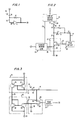
- a typical transimpedance amplifier which is often used in conjunction with optical receivers to provide electrical signals at the front end of the same, comprises inverting amplifier 11 having an input 18 which is connected to a photodiode 10 via lead 16.
- this photodiode is a P-type, Intrinsic, N-type.
- a resistor 13 Also connected in a feedback relationship with the amplifier 11 is a resistor 13.
- An input optical signal 15 is received by photodiode 10 which converts this signal to an electrical signal with AC and DC components.
- the electrical signal is inputted to the inverting amplifier 11 where it is amplified and obtained in inverted form at the output 20.
- the transimpedance amplifier of Fig. 1 is limited in the amount of input current that it can handle by the parameters of the inverting amplifier. For example, there could be a large DC bias on the input signal that would overload the amplifier. In addition, the AC voltage swing at the input 18 could be so large that it saturates the amplifier 11. It would seem possible to shunt away some of the input current of the receiver by use of a resistive device at the input of the receiver. This becomes difficult because the optical receiver typically operates at frequencies (12 MHz for example) where many resistive elements act as capacitors. The feedback resistor 13 and photodiode 10 therefore have parasitic capacitance across them at the operating frequency. Also, there are stray capacitances associated with the amplifier 11. These capacitances cause the amplifier to act as an integrator at high frequencies rather than as an amplifier. Thus it is incumbent that these capacitances be minimized.
- the input current is shunted away by the use of a field effect transistor circuit 23 which has low capacitance at high frequencies and is used as the resistive element to shunt away input current.
- This scheme also incorporates current mirror circuits 21 and 24 for sensing and sinking the DC component of the electrical signal through the FET circuit 23.
- the FET circuit 23 serves two functions: (1) it acts as a large resistance which effectively shunts the DC component of the electrical signal and (2) it provides an AC impedance in response to signals from a peak detector 22 to be later described.
- the improved transimpedance amplifier of Fig. 2 contains a peak detector 22 which detects the output voltage from the inverting amplifier 11.
- This detector 22 has its input end connected to the output 20 of amplifier 11 via lead 32 and its output end connected to the gate of FET 28 in FET circuit 23.
- the drain of FET 28 is connected to the input of amplifier 11 via lead 26 while its source is connected to capacitor 29 which acts as an AC ground for FET circuit 23.
- the current mirrors 21 and 24 are utilized to sense and sink the DC component of the current respectively.
- One end of current mirror 21 is connected to V + where it derives its supply voltage and has one of its legs 34 connected to photodiode 10, and the other leg 25 connected to current mirror 24.
- Current mirror 24 is connected to V- where similarly it derives its supply voltage. Its other leg 33 is electrically connected to the source of FET 28.
- This improved transimpedance amplifier operates in the following manner to shunt the AC component of the electrical signal. It is well known that the AC component of the signal causes a voltage swing at the output 20 of the inverting amplifier 11. This voltage swing which increases with increasing optical signal levels is sensed by peak detector 22. The detector 22 compares the output voltage of the amplifier 11 to a preset reference voltage which corresponds to the normal saturation point of the amplifier 11. When the output voltage of the amplifier 11 approaches this saturation point, the peak detector begins turning on the FET 28 via lead 27. Typically, saturation points for inverting amplifiers are of the order of .1 V peak-to-peak.
- the FET 28 when turned on acts as a variable AC impedance and diverts the input AC component of the electrical signal to ground 30 through capacitor 29.
- the FET circuit 23 also operates to divert the DC component of the electrical signal.
- Current mirror 21 is turned on by the DC component of the electrical signal from photodiode 10. The mirror 21 then provides a DC current proportional to the input photocurrent provided by photodiode 10.
- the current mirror 21 causes the same current to flow in leg 25 that flows in leg 34.
- Leg 33 of current mirror 24 similarly has this current flowing in it and has an electrical connection to FET 28. Therefore, the FET 28 has this same DC component of input current flowing through it as the current sink mirror 24 thereby diverting all DC current to V-.
- V- and V + are -5 and 5 volts respectively.
- the operation of the current sense and sink mirrors can be better understood by referring to Fig. 3.
- the current source mirror 21 comprises a matched pair of transistors 36 and 37 with their bases commonly connected together and to photodiode 10 via lead 34. Their respective emitters are also commonly connected to V + .
- the current sink mirror 24 comprises a pair of matched transistors 38 and 39 with their bases connected in the same way as transistors 36 and 37. Along with the common base connection between the transistors, the collector of transistor 38 is also connected to its base as well as to the collector of transistor 36 via lead 25.
- the DC component of the input current from photodiode 10 turns on transistors 36 and 37 via their respective bases. Equal current thereafter flows through the emitter to collector portions of transistors 36 and 37 through their operation. Since a current is flowing through transistor 36, this same current flows through the leg 25, thereby turning on transistors 38 and 39. The current flowing through transistors 38 and 39 is the same in each transistor because they are a matched transistor pair. This DC current is the same as the current flowing through the FET 28. This current, therefore, flows from the FET 28 through lead 26 and through the current sink to V-. Thus the DC current in effect is diverted from the input of the amplifier by the use of this current mirror sense-sink circuitry and never enters the input of amplifier 11.
- This modification of the transimpedance amplifier improves the dynamic range of the receiver by (1) diverting the DC component of the current through the FET circuit with the current mirrors as the sensing and sinking mechanism, and (2) by limiting AC component of the electrical signal by the use of a peak voltage detector and in conjunction with an FET circuit.
- This modification allows optical transmitters and receivers to be in closer proximity without fear of overloading the receiver.
- the circuit elements necessary for realization of the above described embodiments are readily implemented into a transimpedance amplifier. These improvements will increase the dynamic range of the transimpedance amplifier and at the same time will not appreciably affect the optical sensitivity of the receiver or its performance.
Landscapes
- Physics & Mathematics (AREA)
- Electromagnetism (AREA)
- Engineering & Computer Science (AREA)
- Computer Networks & Wireless Communication (AREA)
- Signal Processing (AREA)
- Power Engineering (AREA)
- Amplifiers (AREA)
Claims (8)
Applications Claiming Priority (2)
| Application Number | Priority Date | Filing Date | Title |
|---|---|---|---|
| US401521 | 1982-07-26 | ||
| US06/401,521 US4498001A (en) | 1982-07-26 | 1982-07-26 | Transimpedance amplifier for optical receivers |
Publications (3)
| Publication Number | Publication Date |
|---|---|
| EP0102174A2 EP0102174A2 (fr) | 1984-03-07 |
| EP0102174A3 EP0102174A3 (en) | 1984-12-27 |
| EP0102174B1 true EP0102174B1 (fr) | 1987-11-11 |
Family
ID=23588102
Family Applications (1)
| Application Number | Title | Priority Date | Filing Date |
|---|---|---|---|
| EP83304205A Expired EP0102174B1 (fr) | 1982-07-26 | 1983-07-20 | Perfectionnements aux amplificateurs de transimpédance ou y relatifs |
Country Status (6)
| Country | Link |
|---|---|
| US (1) | US4498001A (fr) |
| EP (1) | EP0102174B1 (fr) |
| JP (1) | JPH0680989B2 (fr) |
| CA (1) | CA1203293A (fr) |
| DE (1) | DE3374505D1 (fr) |
| GB (1) | GB2124445B (fr) |
Families Citing this family (52)
| Publication number | Priority date | Publication date | Assignee | Title |
|---|---|---|---|---|
| DE3342735A1 (de) * | 1982-11-26 | 1984-05-30 | Tokyo Shibaura Denki K.K., Kawasaki, Kanagawa | Impedanzwandlerschaltung |
| IT1162859B (it) * | 1983-05-12 | 1987-04-01 | Cselt Centro Studi Lab Telecom | Circuito di polarizzazione per circuiti integrati bipolari multifunzione |
| US4565974A (en) * | 1984-08-13 | 1986-01-21 | At&T Bell Laboratories | Optical receiver circuit with active equalizer |
| US4623786A (en) | 1984-11-07 | 1986-11-18 | At&T Bell Laboratories | Transimpedance amplifier with overload protection |
| JPS61228319A (ja) * | 1985-04-03 | 1986-10-11 | Canon Inc | 光電流増幅回路 |
| NL8602408A (nl) * | 1986-09-24 | 1988-04-18 | Philips Nv | Voorversterker voor een optische ontvanger. |
| DE3818168A1 (de) * | 1988-05-26 | 1990-04-05 | Krone Ag | Empfangsvorverstaerker fuer eine optische nachrichtenuebertragungsstrecke |
| US4857725A (en) * | 1988-07-06 | 1989-08-15 | Santa Barbara Research Center | Differential offset corrected current mirror |
| ATE97527T1 (de) * | 1988-09-15 | 1993-12-15 | Siemens Ag | Schaltungsanordnung mit einem an einen optoelektrischen wandler angeschlossenen verstaerker. |
| DE3832857A1 (de) * | 1988-09-28 | 1990-03-29 | Standard Elektrik Lorenz Ag | Optischer empfaenger mit erweitertem dynamikbereich |
| US4889985A (en) * | 1988-10-26 | 1989-12-26 | Tektronix, Inc. | Combined optical power meter and receiver |
| US4902982A (en) * | 1989-02-09 | 1990-02-20 | Hewlett-Packard Company | Nonlinear noninverting transimpedance amplifier |
| GB2233525B (en) * | 1989-06-09 | 1994-02-16 | Stc Plc | Optical receivers |
| JP2546912B2 (ja) * | 1990-05-29 | 1996-10-23 | シャープ株式会社 | 交流増幅器 |
| GB2247798B (en) * | 1990-09-06 | 1994-10-26 | Stc Plc | Optical receiver |
| DE4041761A1 (de) * | 1990-12-24 | 1992-06-25 | Standard Elektrik Lorenz Ag | Stromsenke |
| JPH04367109A (ja) * | 1991-06-13 | 1992-12-18 | Nec Corp | 光通信用前置増幅回路 |
| CA2106439A1 (fr) * | 1992-11-13 | 1994-05-14 | Yusuke Ota | Recepteur de donnees numeriques en salves |
| US5329115A (en) * | 1993-04-29 | 1994-07-12 | International Business Machines Corporation | Optical receiver circuit |
| ES2076077B1 (es) * | 1993-05-31 | 1997-08-16 | Alcatel Standard Electrica | Circuito de control de continua en receptores de datos a rafagas. |
| US5390053A (en) * | 1993-07-22 | 1995-02-14 | Eastman Kodak Company | Circuit for controlling the overall upper cutoff frequency of an amplifier stage |
| GB2288499A (en) * | 1994-03-08 | 1995-10-18 | Stewart Hughes Ltd | Gain control and capacitance correction for photodiode signal amplifier |
| US5734300A (en) * | 1996-05-17 | 1998-03-31 | Lucent Technologies, Inc. | Optical receiver preamplifier dynamic range enhancing circuit and method |
| US5714909A (en) * | 1996-06-14 | 1998-02-03 | Sigmatel, Inc. | Transimpedance amplifier and method for constructing same |
| JPH1140840A (ja) * | 1997-07-16 | 1999-02-12 | Sumitomo Electric Ind Ltd | 光受信器 |
| JPH11127039A (ja) * | 1997-10-24 | 1999-05-11 | Nec Corp | 光受信回路と光受信方法 |
| KR100400379B1 (ko) * | 1997-11-01 | 2003-12-24 | 엘지.필립스 엘시디 주식회사 | 연산증폭기와이를이용한디지털-아날로그변환기 |
| JP3787449B2 (ja) | 1998-01-14 | 2006-06-21 | キヤノン株式会社 | アナログ信号処理回路 |
| US6915083B1 (en) * | 1998-12-15 | 2005-07-05 | Zilog, Inc. | Signal receiver having wide band amplification capability |
| US6624405B1 (en) | 1999-04-19 | 2003-09-23 | Capella Microsystems, Inc. | BIST for testing a current-voltage conversion amplifier |
| US6587003B2 (en) * | 2001-04-18 | 2003-07-01 | Canberra Industries. Inc. | Charge sensitive preamplifier with pulsed source reset |
| US6696887B2 (en) | 2001-09-27 | 2004-02-24 | Matthew S. Taubman | Transistor-based interface circuitry |
| US7068951B2 (en) * | 2002-04-11 | 2006-06-27 | Optical Communication Products, Inc. | Optical signal receiver with RPM, data and data bar output |
| US6798282B1 (en) * | 2002-12-31 | 2004-09-28 | Inphi Corporation | Method and system for transimpedance amplifiers with high current input while maintaining high transimpedance gain and bandwidth |
| US7215883B1 (en) | 2003-01-24 | 2007-05-08 | Jds Uniphase Corporation | Methods for determining the performance, status, and advanced failure of optical communication channels |
| US7002131B1 (en) | 2003-01-24 | 2006-02-21 | Jds Uniphase Corporation | Methods, systems and apparatus for measuring average received optical power |
| US6888123B2 (en) * | 2003-05-09 | 2005-05-03 | Finisar Corporation | Method and apparatus for monitoring a photo-detector |
| RU2269197C1 (ru) * | 2004-05-19 | 2006-01-27 | Валерий Павлович Гузий | Усилитель тока |
| US7332971B2 (en) | 2004-06-10 | 2008-02-19 | Agency For Science, Technology And Research | Multi-gigabit/s transimpedance amplifier for optical networks |
| US7368999B2 (en) * | 2006-07-10 | 2008-05-06 | Jds Uniphase Corporation | DC offset cancellation for a trans-impedance amplifier |
| US20080039035A1 (en) * | 2006-08-10 | 2008-02-14 | Joshua Posamentier | Antenna based listen-before-talk apparatus, system and method |
| KR101401528B1 (ko) * | 2007-06-29 | 2014-06-03 | 가부시키가이샤 한도오따이 에네루기 켄큐쇼 | 광전변환장치 및 그 광전변환장치를 구비하는 전자기기 |
| WO2009014155A1 (fr) * | 2007-07-25 | 2009-01-29 | Semiconductor Energy Laboratory Co., Ltd. | Dispositif de conversion photoélectrique et dispositif électronique comportant celui-ci |
| JP5378519B2 (ja) | 2008-08-07 | 2013-12-25 | ドラム,オウエン | 光学タッチセンサー式デバイスにおけるマルチタッチ事象を検出する方法および装置 |
| US9092092B2 (en) | 2008-08-07 | 2015-07-28 | Rapt Ip Limited | Detecting multitouch events in an optical touch-sensitive device using touch event templates |
| CN101621252B (zh) * | 2009-08-07 | 2012-11-14 | 天津泛海科技有限公司 | 直流恢复与直流监视电路 |
| US8526811B2 (en) * | 2009-10-20 | 2013-09-03 | Sumitomo Electric Device Innovations, U.S.A., Inc. | Power monitoring photodiode array with integrated, current sourced reference photodiode |
| CN104094203B (zh) | 2011-07-22 | 2017-02-15 | 拉普特知识产权公司 | 用于在光学触敏装置中使用的光学耦合器 |
| US9524060B2 (en) | 2012-07-13 | 2016-12-20 | Rapt Ip Limited | Low power operation of an optical touch-sensitive device for detecting multitouch events |
| EP3350919B1 (fr) | 2015-09-15 | 2019-07-31 | Firecomms Limited | Récepteur optique |
| CN110545083B (zh) * | 2018-05-28 | 2024-06-11 | 深圳市芯波微电子有限公司 | 跨阻放大器 |
| US11280674B1 (en) | 2020-09-24 | 2022-03-22 | Veo | Differential trans-impedance amplifier receiver using counter-offset circuitry |
Family Cites Families (5)
| Publication number | Priority date | Publication date | Assignee | Title |
|---|---|---|---|---|
| US3968361A (en) * | 1975-06-23 | 1976-07-06 | The United States Of America As Represented By The Secretary Of The Navy | Laser receiver anti-sun circuit |
| US4057743A (en) * | 1976-04-08 | 1977-11-08 | Rca Corporation | Current sensing circuit |
| US4104533A (en) * | 1977-02-28 | 1978-08-01 | The United States Of America As Represented By The Secretary Of The Navy | Wideband optical isolator |
| US4415803A (en) * | 1980-10-22 | 1983-11-15 | Bell Telephone Laboratories, Incorporated | Optical receiver with improved dynamic range |
| US4540952A (en) * | 1981-09-08 | 1985-09-10 | At&T Bell Laboratories | Nonintegrating receiver |
-
1982
- 1982-07-26 US US06/401,521 patent/US4498001A/en not_active Expired - Lifetime
-
1983
- 1983-07-08 CA CA000432104A patent/CA1203293A/fr not_active Expired
- 1983-07-20 EP EP83304205A patent/EP0102174B1/fr not_active Expired
- 1983-07-20 GB GB08319567A patent/GB2124445B/en not_active Expired
- 1983-07-20 DE DE8383304205T patent/DE3374505D1/de not_active Expired
- 1983-07-26 JP JP58135290A patent/JPH0680989B2/ja not_active Expired - Lifetime
Also Published As
| Publication number | Publication date |
|---|---|
| EP0102174A3 (en) | 1984-12-27 |
| GB8319567D0 (en) | 1983-08-24 |
| JPH0680989B2 (ja) | 1994-10-12 |
| DE3374505D1 (en) | 1987-12-17 |
| US4498001A (en) | 1985-02-05 |
| GB2124445B (en) | 1985-09-11 |
| JPS5934709A (ja) | 1984-02-25 |
| EP0102174A2 (fr) | 1984-03-07 |
| GB2124445A (en) | 1984-02-15 |
| CA1203293A (fr) | 1986-04-15 |
Similar Documents
| Publication | Publication Date | Title |
|---|---|---|
| US4498001A (en) | Transimpedance amplifier for optical receivers | |
| EP0181146B1 (fr) | Amplificateur d'impédance de transfert | |
| US5329115A (en) | Optical receiver circuit | |
| KR100900205B1 (ko) | 넓은 동적 범위 트랜스임피던스 증폭기 | |
| US5844445A (en) | Feedback type pre-amplifier | |
| KR100701741B1 (ko) | 검출 회로 | |
| US4540952A (en) | Nonintegrating receiver | |
| US4805236A (en) | Method and arrangement for increasing the dynamic range at an input stage of an optical receiver | |
| JP3098461B2 (ja) | ディジタル受信回路 | |
| US8248165B2 (en) | Amplifier and optical module performing gain control | |
| US4808810A (en) | Preamplifier for an optical receiver | |
| WO1983004147A1 (fr) | Amplificateur a transistor a effet de champ (fet) a gamme dynamique etendue | |
| EP0402044B1 (fr) | Récepteurs optiques | |
| EP0177216A2 (fr) | Récepteur optique | |
| EP0433468A1 (fr) | Convertisseur de courant en tension | |
| US6876260B2 (en) | Elevated front-end transimpedance amplifier | |
| US7221229B2 (en) | Receiver circuit having an optical reception device | |
| AU621438B2 (en) | Optical receiver including a current limiter | |
| US20050194955A1 (en) | Regulated current mirror | |
| US6686799B2 (en) | Burst mode limiter-amplifier | |
| JPH04225630A (ja) | 広ダイナミックレンジ光受信器 | |
| JP2003163544A (ja) | 帰還増幅回路及びそれを用いた受信装置 | |
| JP3402674B2 (ja) | 光受信用前置増幅器および光受信装置 | |
| JP4389418B2 (ja) | 光受信回路 | |
| JP2002290168A (ja) | 光受信器 |
Legal Events
| Date | Code | Title | Description |
|---|---|---|---|
| PUAI | Public reference made under article 153(3) epc to a published international application that has entered the european phase |
Free format text: ORIGINAL CODE: 0009012 |
|
| AK | Designated contracting states |
Designated state(s): DE FR NL |
|
| PUAL | Search report despatched |
Free format text: ORIGINAL CODE: 0009013 |
|
| AK | Designated contracting states |
Designated state(s): DE FR NL |
|
| 17P | Request for examination filed |
Effective date: 19850529 |
|
| 17Q | First examination report despatched |
Effective date: 19860613 |
|
| GRAA | (expected) grant |
Free format text: ORIGINAL CODE: 0009210 |
|
| AK | Designated contracting states |
Kind code of ref document: B1 Designated state(s): DE FR NL |
|
| REF | Corresponds to: |
Ref document number: 3374505 Country of ref document: DE Date of ref document: 19871217 |
|
| ET | Fr: translation filed | ||
| PLBE | No opposition filed within time limit |
Free format text: ORIGINAL CODE: 0009261 |
|
| STAA | Information on the status of an ep patent application or granted ep patent |
Free format text: STATUS: NO OPPOSITION FILED WITHIN TIME LIMIT |
|
| 26N | No opposition filed | ||
| PGFP | Annual fee paid to national office [announced via postgrant information from national office to epo] |
Ref country code: FR Payment date: 20000622 Year of fee payment: 18 |
|
| PGFP | Annual fee paid to national office [announced via postgrant information from national office to epo] |
Ref country code: NL Payment date: 20000627 Year of fee payment: 18 |
|
| PGFP | Annual fee paid to national office [announced via postgrant information from national office to epo] |
Ref country code: DE Payment date: 20000929 Year of fee payment: 18 |
|
| PG25 | Lapsed in a contracting state [announced via postgrant information from national office to epo] |
Ref country code: NL Free format text: LAPSE BECAUSE OF NON-PAYMENT OF DUE FEES Effective date: 20020201 |
|
| PG25 | Lapsed in a contracting state [announced via postgrant information from national office to epo] |
Ref country code: FR Free format text: LAPSE BECAUSE OF NON-PAYMENT OF DUE FEES Effective date: 20020329 |
|
| NLV4 | Nl: lapsed or anulled due to non-payment of the annual fee |
Effective date: 20020201 |
|
| PG25 | Lapsed in a contracting state [announced via postgrant information from national office to epo] |
Ref country code: DE Free format text: LAPSE BECAUSE OF NON-PAYMENT OF DUE FEES Effective date: 20020501 |
|
| REG | Reference to a national code |
Ref country code: FR Ref legal event code: ST |