EP0102525B1 - Alphateilchenschutz in integrierten Schaltungspackungen - Google Patents
Alphateilchenschutz in integrierten Schaltungspackungen Download PDFInfo
- Publication number
- EP0102525B1 EP0102525B1 EP83107585A EP83107585A EP0102525B1 EP 0102525 B1 EP0102525 B1 EP 0102525B1 EP 83107585 A EP83107585 A EP 83107585A EP 83107585 A EP83107585 A EP 83107585A EP 0102525 B1 EP0102525 B1 EP 0102525B1
- Authority
- EP
- European Patent Office
- Prior art keywords
- film
- conductors
- arms
- hole
- shaped
- Prior art date
- Legal status (The legal status is an assumption and is not a legal conclusion. Google has not performed a legal analysis and makes no representation as to the accuracy of the status listed.)
- Expired
Links
Images
Classifications
-
- H—ELECTRICITY
- H10—SEMICONDUCTOR DEVICES; ELECTRIC SOLID-STATE DEVICES NOT OTHERWISE PROVIDED FOR
- H10W—GENERIC PACKAGES, INTERCONNECTIONS, CONNECTORS OR OTHER CONSTRUCTIONAL DETAILS OF DEVICES COVERED BY CLASS H10
- H10W72/00—Interconnections or connectors in packages
- H10W72/071—Connecting or disconnecting
- H10W72/077—Connecting of TAB connectors
-
- H—ELECTRICITY
- H10—SEMICONDUCTOR DEVICES; ELECTRIC SOLID-STATE DEVICES NOT OTHERWISE PROVIDED FOR
- H10W—GENERIC PACKAGES, INTERCONNECTIONS, CONNECTORS OR OTHER CONSTRUCTIONAL DETAILS OF DEVICES COVERED BY CLASS H10
- H10W42/00—Arrangements for protection of devices
- H10W42/20—Arrangements for protection of devices protecting against electromagnetic or particle radiation, e.g. light, X-rays, gamma-rays or electrons
- H10W42/25—Arrangements for protection of devices protecting against electromagnetic or particle radiation, e.g. light, X-rays, gamma-rays or electrons against alpha rays, e.g. for outer space applications
-
- H—ELECTRICITY
- H10—SEMICONDUCTOR DEVICES; ELECTRIC SOLID-STATE DEVICES NOT OTHERWISE PROVIDED FOR
- H10W—GENERIC PACKAGES, INTERCONNECTIONS, CONNECTORS OR OTHER CONSTRUCTIONAL DETAILS OF DEVICES COVERED BY CLASS H10
- H10W72/00—Interconnections or connectors in packages
- H10W72/701—Tape-automated bond [TAB] connectors
Definitions
- This invention relates to a structure for use in the fabrication of integrated circuits of the type that protect the circuit from alpha-particle radiation.
- Alpha particles are positively charged nuclear particles that are ejected at high speeds by the decay of various radioactive elements, such as uranium or thorium. These radioactive elements are present in very small trace quantities in nearly all materials including those used in integrated circuit packages. Consequently, unless protective steps are taken, the alpha particles will collide with atoms in the integrated circuit to there produce electron-hole pairs. Then if the circuit includes charge-sensitive circuitry, such as a dynamic MOS memory cell, the electron-hole pairs will cause the circuit to malfunction.
- radioactive elements such as uranium or thorium.
- a polyimide shield has been applied over the integrated circuit chip to block the alpha particles from the circuit. See, for example, Electronic Design, November 22, 1980, pp. 36-37 wherein two such shields are described.
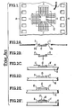
- one shield is formed by depositing liquid polyimide over the surface of the integrated circuit chip and thereafter curing the polyimide; while the other shield is formed by attaching a solid film of polyimide via an adhesive to the surface of the integrated circuit chip. Both prior art methods are illustrated herein via Figures 1 and Figures 2A-2E'.
- a 35 millimeter polyimide tape 10 which has a plurality of electrical conductors 11 disposed thereon. Tape 10 also has a centrally located hole 12; and the conductors 11 extend from the tape in a cantilevered fashion into hole 12. Conductors 11 have their ends arranged in hole 12 such that they align with bumped bonding terminals 13a on the integrated circuit chip 13. The number of electrical conductors 11 and their dimensions vary depending upon the particular chip 13 to which they are to be bonded. Additional sets of conductors 11 and holes 12 are repeated along other portions of tape 10 (not shown); and sprocket holes 14 are provided along the edges of tape 10 so that each set of conductors 11 can be positioned over a chip automatically.
- these steps include the application of several drops of liquid polyimide 17 onto chip 13, and thereafter allowing the liquid to cure.
- these steps include the attaching of a solid polyimide film 17' via an adhesive 18 to chip 13.
- a problem, however, wiht applying liquid polyimide to chip 13 to form the protective shield is that the thickness of the shield is not uniform over the chip's surface. Instead, the shield is much thinner at its perimeter than at its center; and thus, the perimeter of the shield is susceptible to penetration by alpha particles. Also, the thickness of the shield's perimeter cannot be increased simply by applying more polyimide in liquid form to the chip because if the liquid touches the conductors 11', it has a tendency to break those conductors off of the terminals 13a when it cures and hardens.
- a problem with the method of forming the alpha particle shield by attaching the solid polyimide film 17' via an adhesive as illustrated in Figure 2E' is that the alignment of the polyimide film over chip 13 is a very delicate operation. If the film 17' is forced against the conductors 11', it can cause them to break off of the terminals 13a. Consequently, the attaching steps must be performed by hand or by machinery that aligns the film 17' between the terminals 13a very accurately; but this adds to the cost of the package. Also, since the adhesive lies directly on the integrated circuit, it must be highly purified to insure that it doesn't contain any contaminants, such as CL- and NA+, which would migrate from the adhesive into the integrated circuit and cause a malfunction. In addition, the adhesive 18 and the piece of polyimide film 17' are extra materials which further increase the cost of the package.
- one object of the invention is to provide an improved structure for use in fabricating integrated circuits of the type that protect the circuit from alpha-particle radiation.
- Another object of the invention is to provide a structure for use in fabricating integrated circuits such that the fabrication process consists of a reduced number of fabrication steps.
- Still another object of the invention is to provide a structure for use in fabricating integrated circuits such that the fabrication process uses a reduced amount of materials.
- a film of material having a hole which surrounds a central portion of the film and separates it from the remaining film portion.
- the central film portion includes a body with arms extending therefrom.
- a plurality of electrical conductors are disposed on the remaining film portion; and those conductors extend from the remaining film portion across the hole onto the arms of the central film portion to hold it in place. From the arms, the conductors further extend in a cantilevered fashion into the hole towards the body of the central film portion.
- the body portion of the film is shaped to cover a part of the integrated circuit and thereby shield it from alpha particles, while the cantilevered conductors are arranged such that their ends align with contact pads in the integrated circuit outside of the covered portion.
- a film of material having a plurality of holes which are arranged to surround a central portion of the film and separate that central portion from the remaining film portion except for arms of the control portion which extend between the holes.
- a plurality of electrical conductors are disposed on the remaining film portion; and they extend therefrom in a cantilevered fashion into the holes towards the central film portion. At least some of the conductors attach to the arms of the central film portion.
- the central film portion is shaped to cover a part of an integrated circuit and thereby shield it from alpha particles, and the ends of the cantilevered conductors are shaped to align with contact pads in the circuit outside of the covered part.
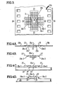
- This embodiment of the invention includes a film of polyimide 20 having a hole 21 which surrounds a central portion 20a of the film and separates it from the remaining film portion 20b.
- Film portion 20a includes a rectangular-shaped body 20a-1 and a pair of T-shaped arms 20a-2 that extend from the body.
- a plurality of electrical conductors 22 are disposed on film portion 20b; and they extend therefrom across hole 21 onto the arms 20a-2 of film portion 20a to hold it in place. From there, the conductors 22 further extend off of the arms 20a-2 in a cantilevered fashion into hole 21 towards the body 20a-1 of film portion 20a.
- Body 20a-1 is shaped to cover a part of an integrated circuit chip 23 and thereby shield it from alpha particles; and the ends of the cantilevered conductors 22 are shaped to align with terminals 23a on chip 23 which lie outside of the covered part.
- Figure 4A illustrates the step in which the conductors 22 are attached to the terminals 23a. During that step, all of the conductors are attached to respective terminals at the same time by a "gang" bond; or alternatively, the conductors are attached one at a time to respective terminals by a "woodpecker" bond. In either case, after the bonding step is complete, body 20a-1 of film portion 20a overlies chip 23 and it is held in place by arms 20a-2.
- conductors 22' are excised from film portion 20b by cutting or punching the conductors 22 around the outer perimeter of hole 21.
- chip 23 is attached via an adhesive 24 to a substrate 25.
- the outer ends of the excised conductors 22' are bonded to corresponding conductors on the substrate.
- An attractive feature of the above-described embodiment of the invention is that it substantively reduces the number of steps that are needed to fabricate an integrated circuit in corn- parison to the prior art. This is evident by comparing the process steps of Figures 4A4D with the corresponding prior art process steps of Figures 2A-2E'. Such a comparison shows that the extra prior art process steps of Figures 2E and 2E' which attach the alpha-particle shield are eliminated. Also, the cost which those extra steps inherently add to the integrated circuit due to their use of extra materials, extra labor, and extra tools to apply the materials is eliminated.
- the Figure 3 embodiment is fabricated by a double-etching process.
- a film of polyimide having a film of copper on one surface thereof is provided.
- this is achieved by casting a polyimide film onto a copper foil; or alternatively it is achieved by depositing copper onto a polyimide film.
- photoresist is deposited on the copper; the resist is patterned to cover only the conductors 22; and the exposed copper is etched completely through so that only the conductors 22 and the polyimide film remain.
- another layer of photoresist is deposited on the polyimide; that resist is patterned to cover only polyimide portions 20a and 20b; and the exposed polyimide is etched completely through to form hole 21 along with sprocket holes 26.
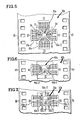
- This embodiment includes a polyimide film 30 having a pair of holes 31 and 32 which almost completely surround a central portion 30a of the film.
- Portion 30a includes a body 30a-1 which is held in place by a pair of arms 30a-2 that extend from the body 30a-1 between the holes 31 and 32 to the remaining portion 30b of the film.
- a plurality of electrical conductors 33 are disposed on film portion 30b and extend therefrom in a cantilevered fashion into holes 31 and 32 toward the body 30a-1. Two of those conductors which lie adjacent the arms 30a-2 also project sideways and attach to the adjacent arms, as is indicated by reference numeral 34.
- Body 30a-1 is shaped to cover a part of an integrated circuit chip and thereby shield it from alpha particles; and the ends of the cantilevered conductors 33 are shaped to align with terminals on the integrated circuit chip which lie outside of the covered part.
- both punching and etching steps are used.
- a polyimide tape having an adhesive film on one side thereof is provided; and that tape is punched to form holes 31 and 32 along with a plurality of sprocket holes 35.
- an electrically conductive film such as one-ounce copper, is attached to the punched tape via the adhesive such that it overlies the holes 31 and 32.
- a layer of photoresist is deposited on the conductive film; the photoresist is patterned so as to cover only conductors 33; and the uncovered portion of the conductive film is etched completely through.
- This embodiment includes a polyimide film 40 having a hole 41 which surrounds a central portion 40a of the film and separates it from the remaining portion 40b thereof.
- Portion has a body 40a-1 which is shaped to cover an integrated circuit and thereby shield it from alpha particles, and it has a pair of C-shaped arms 40a-2 which are joined at their ends to the body.
- a plurality of electrical conductors 42 lie on film portion 40b and they extend therefrom across hole 41 onto the arms 40a-2 to thereby hold film portion 40a in place.
- the conductors 42 extend in a cantilevered fashion towards the body 40a-1 and they are shaped to align with terminals which lie next to the covered portion of the circuit.
- the Figure 6 embodiment is fabricated by the same process steps that were previously described for fabricating the the Figure 3 embodiment.
- This embodiment includes a polyimide film 50 having four holes 51, 52, 53, and 54 which are arranged in a circular fashion to almost completely surround a central portion 50a of the film.
- Portion 50a includes a body 50a-1 which is shaped to cover a part of an integrated circuit and shield it from alpha particles.
- portion 50a includes two C-shaped arms 50a-2 which connect at their ends to the body 50a-1.
- portion 50a includes four straight arms 50a-3 which extend from the body and the C-shaped arms between the holes 51, 52, 53, and 54 to the remaining film portion 50b.
- a plurality of electrical conductors 55 are disposed on film portion 50b and they extend therefrom across the holes 51, 52, 53, and 54 to the C-shaped arms 50a-2. From there, the conductors 55 extend in a cantilevered fashion towards the body 50a-1 such that their ends align with terminals on an integrated circuit chip. Sprocket holes 56 are also provided at the edge of the film.
- this Figure 7 embodiment is fabricated by the process that was described above in conjunction with Figure 3; or alternatively, it can be fabricated by the process that was described above in conjunction with Figure 5.
Landscapes
- Wire Bonding (AREA)
- Semiconductor Integrated Circuits (AREA)
- Structures Or Materials For Encapsulating Or Coating Semiconductor Devices Or Solid State Devices (AREA)
Claims (11)
Applications Claiming Priority (2)
| Application Number | Priority Date | Filing Date | Title |
|---|---|---|---|
| US41062482A | 1982-08-23 | 1982-08-23 | |
| US410624 | 1982-08-23 |
Publications (3)
| Publication Number | Publication Date |
|---|---|
| EP0102525A2 EP0102525A2 (de) | 1984-03-14 |
| EP0102525A3 EP0102525A3 (en) | 1986-01-15 |
| EP0102525B1 true EP0102525B1 (de) | 1988-07-06 |
Family
ID=23625526
Family Applications (1)
| Application Number | Title | Priority Date | Filing Date |
|---|---|---|---|
| EP83107585A Expired EP0102525B1 (de) | 1982-08-23 | 1983-08-02 | Alphateilchenschutz in integrierten Schaltungspackungen |
Country Status (3)
| Country | Link |
|---|---|
| EP (1) | EP0102525B1 (de) |
| JP (1) | JPS59134858A (de) |
| DE (1) | DE3377313D1 (de) |
Cited By (1)
| Publication number | Priority date | Publication date | Assignee | Title |
|---|---|---|---|---|
| WO2015023312A3 (en) * | 2013-05-16 | 2015-04-16 | National Institute Of Aerospace Associates | Radiation hardened microelectronic chip packaging technology |
Families Citing this family (1)
| Publication number | Priority date | Publication date | Assignee | Title |
|---|---|---|---|---|
| DE3910710A1 (de) * | 1989-04-03 | 1990-10-04 | Standard Elektrik Lorenz Ag | Optisch-elektrische mehrfachverbindung |
Family Cites Families (4)
| Publication number | Priority date | Publication date | Assignee | Title |
|---|---|---|---|---|
| FR2311406A1 (fr) * | 1975-05-13 | 1976-12-10 | Honeywell Bull Soc Ind | Perfectionnements aux procedes de fabrication de supports de conditionnement de micro-plaquettes de circuits integres |
| JPS5568659A (en) * | 1978-11-20 | 1980-05-23 | Hitachi Ltd | Semiconductor device and manufacturing method thereof |
| JPS577144A (en) * | 1980-06-17 | 1982-01-14 | Fujitsu Ltd | Semiconductor device |
| US4380566A (en) * | 1981-07-13 | 1983-04-19 | Fairchild Camera & Instrument Corp. | Radiation protection for integrated circuits utilizing tape automated bonding |
-
1983
- 1983-08-02 DE DE8383107585T patent/DE3377313D1/de not_active Expired
- 1983-08-02 EP EP83107585A patent/EP0102525B1/de not_active Expired
- 1983-08-16 JP JP58150099A patent/JPS59134858A/ja active Pending
Cited By (1)
| Publication number | Priority date | Publication date | Assignee | Title |
|---|---|---|---|---|
| WO2015023312A3 (en) * | 2013-05-16 | 2015-04-16 | National Institute Of Aerospace Associates | Radiation hardened microelectronic chip packaging technology |
Also Published As
| Publication number | Publication date |
|---|---|
| JPS59134858A (ja) | 1984-08-02 |
| EP0102525A3 (en) | 1986-01-15 |
| DE3377313D1 (en) | 1988-08-11 |
| EP0102525A2 (de) | 1984-03-14 |
Similar Documents
| Publication | Publication Date | Title |
|---|---|---|
| US5892271A (en) | Semiconductor device | |
| US4661837A (en) | Resin-sealed radiation shield for a semiconductor device | |
| US5710064A (en) | Method for manufacturing a semiconductor package | |
| US6107679A (en) | Semiconductor device | |
| US6774467B2 (en) | Semiconductor device and process of production of same | |
| DE69028334T2 (de) | Herstellungsverfähren für elektronische Module | |
| DE69015969T2 (de) | Packung eines Hochfrequenz-Transistors mit Nickeloxidschutzschicht. | |
| GB2047474A (en) | A strip carrying devices for processing electrical signals, and a method of producing the strip | |
| DE19904258A1 (de) | Halbleitervorrichtung | |
| US5016084A (en) | Semiconductor device | |
| US6175152B1 (en) | Semiconductor device | |
| EP0102525A2 (de) | Alphateilchenschutz in integrierten Schaltungspackungen | |
| US6627986B2 (en) | Substrate for semiconductor device and semiconductor device fabrication using the same | |
| JPS614249A (ja) | 半導体装置用パツケ−ジ | |
| EP0413161B1 (de) | Leitfähige Verbindungsstruktur | |
| KR100257404B1 (ko) | 반도체 패키지 및 반도체 패키지의 입출력선 형성방법 | |
| EP0526147B1 (de) | Halbleiteranordnung vom Filmträgertyp und Verfahren zum Herstellen derselben | |
| KR100319400B1 (ko) | 반도체패키지및그제조방법 | |
| US20250218927A1 (en) | Flat package | |
| US20240266295A1 (en) | Electronic package module and method for fabrication of the same | |
| JP2630294B2 (ja) | 混成集積回路装置およびその製造方法 | |
| KR100710133B1 (ko) | 반도체 패키지용 인쇄회로기판 | |
| JP2555878B2 (ja) | フィルムキャリヤーテープの製造方法 | |
| JPH04164345A (ja) | 樹脂封止半導体装置およびその製造方法 | |
| JPS5951555A (ja) | 半導体集積回路装置 |
Legal Events
| Date | Code | Title | Description |
|---|---|---|---|
| PUAI | Public reference made under article 153(3) epc to a published international application that has entered the european phase |
Free format text: ORIGINAL CODE: 0009012 |
|
| AK | Designated contracting states |
Designated state(s): BE DE FR GB NL SE |
|
| PUAL | Search report despatched |
Free format text: ORIGINAL CODE: 0009013 |
|
| AK | Designated contracting states |
Designated state(s): BE DE FR GB NL SE |
|
| 17P | Request for examination filed |
Effective date: 19860129 |
|
| RAP1 | Party data changed (applicant data changed or rights of an application transferred) |
Owner name: BURROUGHS CORPORATION (A DELAWARE CORPORATION) |
|
| 17Q | First examination report despatched |
Effective date: 19870515 |
|
| GRAA | (expected) grant |
Free format text: ORIGINAL CODE: 0009210 |
|
| AK | Designated contracting states |
Kind code of ref document: B1 Designated state(s): BE DE FR GB NL SE |
|
| REF | Corresponds to: |
Ref document number: 3377313 Country of ref document: DE Date of ref document: 19880811 |
|
| ET | Fr: translation filed | ||
| PLBE | No opposition filed within time limit |
Free format text: ORIGINAL CODE: 0009261 |
|
| STAA | Information on the status of an ep patent application or granted ep patent |
Free format text: STATUS: NO OPPOSITION FILED WITHIN TIME LIMIT |
|
| 26N | No opposition filed | ||
| PGFP | Annual fee paid to national office [announced via postgrant information from national office to epo] |
Ref country code: GB Payment date: 19930708 Year of fee payment: 11 |
|
| PGFP | Annual fee paid to national office [announced via postgrant information from national office to epo] |
Ref country code: SE Payment date: 19930719 Year of fee payment: 11 |
|
| PGFP | Annual fee paid to national office [announced via postgrant information from national office to epo] |
Ref country code: FR Payment date: 19930808 Year of fee payment: 11 |
|
| PGFP | Annual fee paid to national office [announced via postgrant information from national office to epo] |
Ref country code: DE Payment date: 19930825 Year of fee payment: 11 |
|
| PGFP | Annual fee paid to national office [announced via postgrant information from national office to epo] |
Ref country code: NL Payment date: 19930831 Year of fee payment: 11 |
|
| PGFP | Annual fee paid to national office [announced via postgrant information from national office to epo] |
Ref country code: BE Payment date: 19930910 Year of fee payment: 11 |
|
| PG25 | Lapsed in a contracting state [announced via postgrant information from national office to epo] |
Ref country code: GB Effective date: 19940802 |
|
| PG25 | Lapsed in a contracting state [announced via postgrant information from national office to epo] |
Ref country code: SE Effective date: 19940803 |
|
| PG25 | Lapsed in a contracting state [announced via postgrant information from national office to epo] |
Ref country code: BE Effective date: 19940831 |
|
| EAL | Se: european patent in force in sweden |
Ref document number: 83107585.8 |
|
| BERE | Be: lapsed |
Owner name: BURROUGHS CORP. Effective date: 19940831 |
|
| PG25 | Lapsed in a contracting state [announced via postgrant information from national office to epo] |
Ref country code: NL Effective date: 19950301 |
|
| GBPC | Gb: european patent ceased through non-payment of renewal fee |
Effective date: 19940802 |
|
| NLV4 | Nl: lapsed or anulled due to non-payment of the annual fee | ||
| PG25 | Lapsed in a contracting state [announced via postgrant information from national office to epo] |
Ref country code: FR Effective date: 19950428 |
|
| PG25 | Lapsed in a contracting state [announced via postgrant information from national office to epo] |
Ref country code: DE Effective date: 19950503 |
|
| EUG | Se: european patent has lapsed |
Ref document number: 83107585.8 |
|
| REG | Reference to a national code |
Ref country code: FR Ref legal event code: ST |