EP0103023B1 - Halbleiterbildaufzeichnungsvorrichtung - Google Patents
Halbleiterbildaufzeichnungsvorrichtung Download PDFInfo
- Publication number
- EP0103023B1 EP0103023B1 EP83900653A EP83900653A EP0103023B1 EP 0103023 B1 EP0103023 B1 EP 0103023B1 EP 83900653 A EP83900653 A EP 83900653A EP 83900653 A EP83900653 A EP 83900653A EP 0103023 B1 EP0103023 B1 EP 0103023B1
- Authority
- EP
- European Patent Office
- Prior art keywords
- transfer
- photodetectors
- period
- image pick
- portions
- Prior art date
- Legal status (The legal status is an assumption and is not a legal conclusion. Google has not performed a legal analysis and makes no representation as to the accuracy of the status listed.)
- Expired
Links
Images

Classifications
-
- H—ELECTRICITY
- H10—SEMICONDUCTOR DEVICES; ELECTRIC SOLID-STATE DEVICES NOT OTHERWISE PROVIDED FOR
- H10F—INORGANIC SEMICONDUCTOR DEVICES SENSITIVE TO INFRARED RADIATION, LIGHT, ELECTROMAGNETIC RADIATION OF SHORTER WAVELENGTH OR CORPUSCULAR RADIATION
- H10F39/00—Integrated devices, or assemblies of multiple devices, comprising at least one element covered by group H10F30/00, e.g. radiation detectors comprising photodiode arrays
- H10F39/10—Integrated devices
- H10F39/12—Image sensors
- H10F39/15—Charge-coupled device [CCD] image sensors
- H10F39/158—Charge-coupled device [CCD] image sensors having arrangements for blooming suppression
-
- H—ELECTRICITY
- H10—SEMICONDUCTOR DEVICES; ELECTRIC SOLID-STATE DEVICES NOT OTHERWISE PROVIDED FOR
- H10F—INORGANIC SEMICONDUCTOR DEVICES SENSITIVE TO INFRARED RADIATION, LIGHT, ELECTROMAGNETIC RADIATION OF SHORTER WAVELENGTH OR CORPUSCULAR RADIATION
- H10F39/00—Integrated devices, or assemblies of multiple devices, comprising at least one element covered by group H10F30/00, e.g. radiation detectors comprising photodiode arrays
- H10F39/10—Integrated devices
- H10F39/12—Image sensors
- H10F39/15—Charge-coupled device [CCD] image sensors
- H10F39/153—Two-dimensional or three-dimensional array CCD image sensors
Definitions
- This invention relates to solid-state image pick-up apparatus comprising a solid state image pick-up device.
- Solid state image pick-up devices comprising a charge transfer device such as a charge coupled device (CCD) are classified broadly into the frame transfer type and the interline transfer type.
- CCD charge coupled device
- FIG. 1 An example of a solid state image pick-up device of the interline transfer type using a CCD is shown in Figure 1, and comprises a photosensing and vertical transfer portion 3 which includes a plurality of photodetectors 1 arranged in horizontal and vertical rows, and vertical transfer portions 2 each formed with a group of CCDs along each of the vertical rows of photodetectors 1, a horizontal transfer portion 4 coupled with the photo-sensing and vertical transfer portion 3, and an output portion 5 coupled with the horizontal transfer portion 4 and provided with a signal output terminal 5a, all formed on a common semiconductor substrate.
- a photosensing and vertical transfer portion 3 which includes a plurality of photodetectors 1 arranged in horizontal and vertical rows, and vertical transfer portions 2 each formed with a group of CCDs along each of the vertical rows of photodetectors 1, a horizontal transfer portion 4 coupled with the photo-sensing and vertical transfer portion 3, and an output portion 5 coupled with the horizontal transfer portion 4 and provided with a signal output terminal 5a, all formed on a common semiconductor substrate
- predetermined vertical and horizontal transfer driving signals are applied to the vertical and horizontal transfer portions 2 and 4 respectively, so that vertical and horizontal charge transfers are performed.
- Signal charge obtained in the photodetectors 1 in response to the light received thereby during, for example one frame period is read out to the vertical transfer portions 2 and then transferred vertically towards the horizontal transfer portion 4 during each horizontal blanking period, so that the signal charge produced in each horizontal row of the photodetectors 1 is transferred in turn to the horizontal transfer portion 4.
- This signal charge is further transferred horizonally to the output portion 5 by the charge transfer operation of the horizontal transfer portion 4 during each horizontal video period, and as a result of this an image pick-up signal output is obtained at the terminal 5a.
- the photo-sensing and vertical transfer portion 3 contains transfer gate areas 6 between row of photodetectors 1 and the corresponding one of the vertical transfer portions 2, and a channel stop area 7 and an overflow control gate portion 8 around each of the photodetectors 1, as shown in Figure 2.
- An overflow drain 9 is provided contiguous to each of the overflow control gate portions 8, and each of the overflow drains 9 and the corresponding one of the vertical transfer portions 2 are separated by a channel stop area 10.
- These various areas and portions are covered by an insulating layer on which vertical transfer electrodes ⁇ 1 and ⁇ 2 each elongated in the horizontal direction are provided alternately in the vertical direction at the areas corresponding to the vertical transfer portions 2.
- Each vertical transfer electrode ⁇ 1 comprises a charge storage electrode ⁇ 1c and a charge transfer electrode potential barrier electrode) ⁇ 1t
- each vertical transfer electrode ⁇ 2 comprises a charge storage electrode ⁇ 2c and a charge transfer electrode ⁇ 2t.
- storage regions are formed under the charge storage electrodes ⁇ 1c and (p2c
- transfer regions are formed under the charge transfer electrodes ⁇ 1t and ( p 2t, and each transfer region is subjected to ion implantation or provided thereon with a thick insulating layer so as to have a potential shallower (lower) than that of the storage region adjacent thereto, and to form a potential barrier.
- a transfer gate electrode T extending in the vertical direction is provided on each group of transfer gate areas 6 aligned in the vertical direction, and an overflow control gate electrode OG also extending in the vertical directions is provided on each overflow control gate portion 8.
- a light shielding layer 11 is also provided on these various areas and portions except the areas of the photodetectors 1 to form a light shielded portion.
- a predetermined gating signal cpt is supplied to the transfer gate electrodes T so that a transfer gate voltage is applied selectively to the transfer gate areas 6, and a predetermined bias voltage is supplied through the overflow control gate electrodes OG to the overflow control gate portions 8.
- the vertical transfer electrodes (p1 and ⁇ 2 are supplied with two-phase driving signals cp1 and cp2, respectively, and the voltages of the driving signals cp1 and cp2 are applied to the vertical transfer portions 2 positioned under the vertical transfer electrodes ⁇ 1 and ⁇ 2.
- the portion where the light from an object is received is limited to the photodetectors on which no light shielding layer is provided and therefore the light receiving aperture ratio, that is, the ratio of the light receiving area to the whole area of the photo-sensing and vertical transfer portion 3 is quite low.
- the photo-sensitivity of the device is low, and especially in the case of operation for producing an image pick-up signal output representing a still image, in which the light is received for a short period during which a shutter mechanism for the photo- sensing and vertical transfer portion 3 is open, and the image pick-up output signal is obtained in response to signal charge stored in the photo- dioses 1 during such a short period, an image pick-up signal output with sufficient dynamic range and a good signal-to-noise ratio cannot be obtained.
- a solid state image pick-up apparatus comprising a solid state image pick-up device of the interline transfer type having photodetectors for producing signal charge in response to the light received thereby and storing the signal charge produced therein, transfer portions for transferring the signal charge read out from the photodetectors, and transfer gate areas provided between the photodetectors, and transfer portions for reading out the signal charge from the photodetectors to the corresponding transfer portions, and being formed such that the photodetectors and the transfer portions are not covered with a light shielding layer, and a shutter mechanism associated with the solid state image pick-up device, wherein the shutter mechanism is made open and the relationship of Pr- ⁇ Pt ⁇ Ps, where Ps, Pt and Pr are the potentials of the photodetector, the corresponding transfer gate area and the corresponding transfer portion, respectively, is maintained during a light receiving period, the shutter mechanism is shut and the relationship of Ps--Pt ⁇ Pr is maintained during a reading out period, and the shutter mechanism is shut and the relationship of
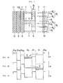
- the solid state image pick-up device of the interline transfer type having a portion thereof as shown in Figure 3 comprises a CCD and has the ame configuration as that of Figure 1.
- photodetectors 1 vertical transfer portions 2, transfer gate areas 6, channel stop areas 7, overflow control gate portions 8, overflow drains 9 and channel stop areas 10 are shown as in Figure 2
- vertical transfer electrodes ⁇ 1 each comprising a charge storage electrode ⁇ 1c and a charge transfer electrode ⁇ lt
- vertical transfer electrodes q)2 each comprising a charge storage electrode ⁇ 2c and a charge transfer electrode 02t
- transfer gate electrodes T and overflow control gate electrodes OG are provided as in Figure 2.
- the photo-sensing and vertical transfer portion shown in Figure 3 has a light shielded portion different from that in Figure 2.
- a light shielding layer 11 is provided only on the overflow control gate portion 8, the overflow drain 9 and the channel stop area 10 to form the light shielded portion. Accordingly, the vertical transfer portion 2, the transfer gate area 6 and the channel stop area 7 form respective light receiving portions, not covered by the light shielding layer 11, in addition to the photodetector 1.
- the solid state image pick-up apparatus embodying the present invention has such a solid state pick-up device and a shutter mechanism for limiting the light entering the photo-sensing and vertical transfer portion so as to produce an image pick-up signal output representing a still image.
- the potential of each portion or area in the photo-sensing and vertical transfer portion is controlled.
- the relationship between the potentials of portions and areas in the photo-sensing and vertical transfer portion is as shown in Figure 4A, where Ps stands for the potential of the photodetector 1, Pr stands for the potential of the vertical transfer portion 2, Pt stands for the potential of the transfer gate area 6, Pog stands for the potential of the overflow control gate portion 8, Pod stands for the potential of the overflow drain 9, and Pcs stands for the potential of the channel stop area 10.
- each of the potentials Ps, Pog, Pod and Pcs of the phototdetector 1, the overflow control gate portion 8, the overflow drain 9 and the channel stop area, respectively, is maintained constant throughout the light receiving period, the reading out period and the charge transfer period, and the relationhip Pcs ⁇ Pog ⁇ Ps ⁇ Pod is maintained. Accordingly, when charge which exceeds the potential barrier by the potential Pog is produced in the photodetectors 1, such excessive charge overflows into the overflow drain 9 to be drained therethrough.
- both the potential Pr of the vertical transfer portion 2 and the potential Pt of the transfer gate area 6 vary in response to the voltages of the driving signals cp1 and cp2 supplied to the vertical transfer electrodes ⁇ 1 and q )2 and the gating voltage resulting from the gating signal cpt supplied to the transfer gate electrode T, respectively.
- the relationship Pr ⁇ Pt ⁇ Ps is maintained, as shown in Figure 4A.
- the charge produced in the vertical transfer portions 2 and the transfer gate areas 6 becomes signal charge in addition to the charge produced in the photodetectors 1, and the vertical transfer portions 2 in particular act as a light receiving portion having a relatively large area, so that the signal charge produced in response to the light entering the photo-sensing and vertical transfer portion is substantially increased. That is, the light receiving aperture ratio is substantially increased and therefore the photo-sensitivity is improved.
- the relationship Pt ⁇ Ps, Pt ⁇ Pr is maintained, and the potential Pr varies between a high level and a low level in response to vertical transfer pulses in the driving signals cp1 and cp2, so that the signal charge Q is transferred to the horizontal transfer portion 4 from the vertical transfer portions 2 during each period corresponding to the horizontal blanking period.
- the signal charge Q transferred to the horizontal blanking period transfer portion 4 during each period corresponding to the horizontal blanking period is further transferred to the output portion 5 from the horizontal transfer portion 4 during each period corresponding to the horizontal video period, and as a result of this, an image pick-up signal output representing a still image is obtained at the terminal 5a in the form of successive segments each corresponding to one field period.
- the vertical transfer electrodes ⁇ 1 and ⁇ 2 cause the vertical charge transfer to be performed in the two-phase transfer mode with two-phase driving signals
- other overflow drains formed in a different manner can be provided.
- Embodiments of the invention can produce an image pick-up signal output representing a high- shuttering speed still image with enlarged dynamic range and an improved signal-to-noise ratio with low smear and bloom, and are therefore suitable for high-grade, miniature, lightweight still television cameras.
Landscapes
- Solid State Image Pick-Up Elements (AREA)
- Transforming Light Signals Into Electric Signals (AREA)
Claims (2)
Applications Claiming Priority (2)
| Application Number | Priority Date | Filing Date | Title |
|---|---|---|---|
| JP57025731A JPS58142570A (ja) | 1982-02-19 | 1982-02-19 | 固体撮像装置 |
| JP25731/82 | 1982-02-19 |
Publications (3)
| Publication Number | Publication Date |
|---|---|
| EP0103023A1 EP0103023A1 (de) | 1984-03-21 |
| EP0103023A4 EP0103023A4 (de) | 1986-01-07 |
| EP0103023B1 true EP0103023B1 (de) | 1988-10-05 |
Family
ID=12173949
Family Applications (1)
| Application Number | Title | Priority Date | Filing Date |
|---|---|---|---|
| EP83900653A Expired EP0103023B1 (de) | 1982-02-19 | 1983-02-10 | Halbleiterbildaufzeichnungsvorrichtung |
Country Status (5)
| Country | Link |
|---|---|
| US (1) | US4605862A (de) |
| EP (1) | EP0103023B1 (de) |
| JP (1) | JPS58142570A (de) |
| DE (1) | DE3378174D1 (de) |
| WO (1) | WO1983003031A1 (de) |
Families Citing this family (10)
| Publication number | Priority date | Publication date | Assignee | Title |
|---|---|---|---|---|
| JPS61176150A (ja) * | 1985-01-31 | 1986-08-07 | Toshiba Corp | 固体撮像装置 |
| US4758895A (en) * | 1985-11-12 | 1988-07-19 | Rca Corporation | Storage registers with charge packet accumulation capability, as for solid-state imagers |
| JPS6374377A (ja) * | 1986-09-18 | 1988-04-04 | Fuji Photo Film Co Ltd | ブル−ミング抑制方法 |
| JPS62245874A (ja) * | 1986-04-18 | 1987-10-27 | Fuji Photo Film Co Ltd | 固体撮像装置 |
| US4875100A (en) * | 1986-10-23 | 1989-10-17 | Sony Corporation | Electronic shutter for a CCD image sensor |
| JPS63256068A (ja) * | 1987-04-14 | 1988-10-24 | Fuji Electric Co Ltd | Ccd型固体撮像素子を用いた撮像方法 |
| JPH07112059B2 (ja) * | 1989-02-03 | 1995-11-29 | シャープ株式会社 | 固体撮像装置 |
| US6366322B1 (en) | 1991-04-15 | 2002-04-02 | Lg Semicon Co., Ltd. | Horizontal charge coupled device of CCD image sensor |
| JPH05260389A (ja) * | 1991-12-20 | 1993-10-08 | Eastman Kodak Co | 画像捕捉装置 |
| JP2017537046A (ja) | 2014-10-20 | 2017-12-14 | ピルキントン グループ リミテッド | 複層ガラスユニット |
Family Cites Families (7)
| Publication number | Priority date | Publication date | Assignee | Title |
|---|---|---|---|---|
| US3896474A (en) * | 1973-09-10 | 1975-07-22 | Fairchild Camera Instr Co | Charge coupled area imaging device with column anti-blooming control |
| JPS5451318A (en) * | 1977-09-29 | 1979-04-23 | Sony Corp | Solid pickup unit |
| JPS5531333A (en) * | 1978-08-28 | 1980-03-05 | Sony Corp | Solid state pickup device |
| JPS5685981A (en) * | 1979-12-15 | 1981-07-13 | Sharp Corp | Solid image pickup apparatus |
| JPS56136076A (en) * | 1980-03-26 | 1981-10-23 | Hitachi Ltd | Photoelectric converter |
| US4354104A (en) * | 1980-05-06 | 1982-10-12 | Matsushita Electric Industrial Co., Ltd. | Solid-state image pickup device |
| JPS5819080A (ja) * | 1981-07-27 | 1983-02-03 | Sony Corp | 固体撮像素子 |
-
1982
- 1982-02-19 JP JP57025731A patent/JPS58142570A/ja active Pending
-
1983
- 1983-02-10 EP EP83900653A patent/EP0103023B1/de not_active Expired
- 1983-02-10 US US06/557,169 patent/US4605862A/en not_active Expired - Lifetime
- 1983-02-10 DE DE8383900653T patent/DE3378174D1/de not_active Expired
- 1983-02-10 WO PCT/JP1983/000040 patent/WO1983003031A1/ja not_active Ceased
Also Published As
| Publication number | Publication date |
|---|---|
| WO1983003031A1 (fr) | 1983-09-01 |
| EP0103023A1 (de) | 1984-03-21 |
| JPS58142570A (ja) | 1983-08-24 |
| EP0103023A4 (de) | 1986-01-07 |
| US4605862A (en) | 1986-08-12 |
| DE3378174D1 (en) | 1988-11-10 |
Similar Documents
| Publication | Publication Date | Title |
|---|---|---|
| US5446493A (en) | Solid state image sensors for reproducing high definition images | |
| US6452634B1 (en) | Charge transfer device and method of driving the same, and solid state imaging device and method of driving the same | |
| EP0103023B1 (de) | Halbleiterbildaufzeichnungsvorrichtung | |
| JPH0414546B2 (de) | ||
| US5280186A (en) | CCD image sensor with four phase clocking mechanism | |
| US5757427A (en) | Image pick-up apparatus having a charge coupled device with multiple electrodes, a buffer layer located below some of the electrodes | |
| EP0086845B1 (de) | Halbleiter-bildaufnahmevorrichtung | |
| EP0088134B1 (de) | Integrierte bildaufnahmevorrichtung | |
| EP0083376A1 (de) | Festkörper-bildaufnahmeeinrichtung | |
| KR101293586B1 (ko) | 고체촬상장치 및 고체촬상장치의 구동방법 | |
| US5283633A (en) | Solid state image pickup device in which picture elements of green are generated in vertical charge transfer paths | |
| JP2697246B2 (ja) | 固体撮像素子 | |
| JPH01125074A (ja) | 固体撮像装置 | |
| JP2872476B2 (ja) | 固体撮像装置とその駆動方法 | |
| JP2616672B2 (ja) | 撮像装置 | |
| JPH0773347B2 (ja) | 固体撮像装置の駆動方法 | |
| KR20250031730A (ko) | 이미지 센싱 장치 | |
| JPH0473347B2 (de) | ||
| JPH07226497A (ja) | 固体撮像素子 | |
| JP2684377B2 (ja) | カラー用固体撮像素子 | |
| KR960006200B1 (ko) | 고체 촬상장치 및 그 제조방법 | |
| JPS63234677A (ja) | 電荷結合素子の駆動方法 | |
| JPH05183820A (ja) | Ccd型固体撮像素子 | |
| JPS6089177A (ja) | 撮像素子 | |
| JPH0771232B2 (ja) | 固体撮像装置 |
Legal Events
| Date | Code | Title | Description |
|---|---|---|---|
| PUAI | Public reference made under article 153(3) epc to a published international application that has entered the european phase |
Free format text: ORIGINAL CODE: 0009012 |
|
| 17P | Request for examination filed |
Effective date: 19831104 |
|
| AK | Designated contracting states |
Designated state(s): DE FR GB NL |
|
| 17Q | First examination report despatched |
Effective date: 19870818 |
|
| GRAA | (expected) grant |
Free format text: ORIGINAL CODE: 0009210 |
|
| AK | Designated contracting states |
Kind code of ref document: B1 Designated state(s): DE FR GB NL |
|
| REF | Corresponds to: |
Ref document number: 3378174 Country of ref document: DE Date of ref document: 19881110 |
|
| ET | Fr: translation filed | ||
| PLBE | No opposition filed within time limit |
Free format text: ORIGINAL CODE: 0009261 |
|
| STAA | Information on the status of an ep patent application or granted ep patent |
Free format text: STATUS: NO OPPOSITION FILED WITHIN TIME LIMIT |
|
| 26N | No opposition filed | ||
| PGFP | Annual fee paid to national office [announced via postgrant information from national office to epo] |
Ref country code: FR Payment date: 19921229 Year of fee payment: 11 |
|
| PGFP | Annual fee paid to national office [announced via postgrant information from national office to epo] |
Ref country code: GB Payment date: 19930209 Year of fee payment: 11 |
|
| PGFP | Annual fee paid to national office [announced via postgrant information from national office to epo] |
Ref country code: NL Payment date: 19930228 Year of fee payment: 11 |
|
| PGFP | Annual fee paid to national office [announced via postgrant information from national office to epo] |
Ref country code: DE Payment date: 19930429 Year of fee payment: 11 |
|
| PG25 | Lapsed in a contracting state [announced via postgrant information from national office to epo] |
Ref country code: GB Effective date: 19940210 |
|
| PG25 | Lapsed in a contracting state [announced via postgrant information from national office to epo] |
Ref country code: NL Effective date: 19940901 |
|
| GBPC | Gb: european patent ceased through non-payment of renewal fee |
Effective date: 19940210 |
|
| NLV4 | Nl: lapsed or anulled due to non-payment of the annual fee | ||
| PG25 | Lapsed in a contracting state [announced via postgrant information from national office to epo] |
Ref country code: FR Effective date: 19941031 |
|
| PG25 | Lapsed in a contracting state [announced via postgrant information from national office to epo] |
Ref country code: DE Effective date: 19941101 |
|
| REG | Reference to a national code |
Ref country code: FR Ref legal event code: ST |