EP0105755A2 - Selektiver Zugriff in Datenverarbeitungsanlagen - Google Patents
Selektiver Zugriff in Datenverarbeitungsanlagen Download PDFInfo
- Publication number
- EP0105755A2 EP0105755A2 EP83305969A EP83305969A EP0105755A2 EP 0105755 A2 EP0105755 A2 EP 0105755A2 EP 83305969 A EP83305969 A EP 83305969A EP 83305969 A EP83305969 A EP 83305969A EP 0105755 A2 EP0105755 A2 EP 0105755A2
- Authority
- EP
- European Patent Office
- Prior art keywords
- address
- bus
- signal
- integrated circuit
- semiconductor integrated
- Prior art date
- Legal status (The legal status is an assumption and is not a legal conclusion. Google has not performed a legal analysis and makes no representation as to the accuracy of the status listed.)
- Granted
Links
Images



Classifications
-
- G—PHYSICS
- G06—COMPUTING OR CALCULATING; COUNTING
- G06F—ELECTRIC DIGITAL DATA PROCESSING
- G06F12/00—Accessing, addressing or allocating within memory systems or architectures
- G06F12/02—Addressing or allocation; Relocation
- G06F12/06—Addressing a physical block of locations, e.g. base addressing, module addressing, memory dedication
- G06F12/0646—Configuration or reconfiguration
- G06F12/0669—Configuration or reconfiguration with decentralised address assignment
- G06F12/0676—Configuration or reconfiguration with decentralised address assignment the address being position dependent
Definitions
- the present invention relates to selective accessing in data processing systems, for example to a system including a semiconductor IC device such as an IC chip of a memory device or an input/output (I/O) control device which is selected and used by an address signal from a central processing unit (CPU).
- a semiconductor IC device such as an IC chip of a memory device or an input/output (I/O) control device which is selected and used by an address signal from a central processing unit (CPU).
- CPU central processing unit
- peripheral circuits such as memory devices and/or I/O control devices are used.
- Each of the peripheral circuits is constituted of, for example, one peripheral large scale integration (LSI) chip and comprises a memory device or an I/O control circuit which control various I/O devices.
- LSI peripheral large scale integration
- each peripheral LSI is absolutely determined in correspondence to the structure of the address decoder.
- programs designed for one computer system may not be compatible with other computer systemsusing the same CPU, because the addresses of the peripheral LSI's do not coincide withtho B e of the former computer system. Therefore, software of computer systems using conventional peripheral IC's are not usually interchangeable.
- An embodiment of the present invention can provide an address memory for storing the address of a peripheral IC chip and a comparator within the peripheral IC chip itself, which can enable itself on the basis of address data from a CPU.
- An embodiment of the present invention can provide a semiconductor IC device used in a data processing system characterized in that the device comprises an address memory for storing the chip address of the device itself and a comparator for comparing an address signal input thereto from an external circuit and the content of the address memory. Address data existing on a bus line in an initial setting status is previously stored in the address memory as a chip address of the device. The device enters a chip selected condition depending on the coincidence between an address dignal input thereto from an external circuit and the content of the address memory.
- the system of Fig. 1 comprises a CPU 1, an address decoder 2, and peripheral LSI's 3 and 4.
- the address decoder 2 constitutes an interface circuit of the CPU 1, the peripheral LSI's 3 and 4, and so on.
- the peripheral LSI's 3 and 4 and so on are, for example, memory devices, I/O control devices, and so on.
- an address signal from the CPU 1 is input to the address decoder 2 via an address bus.
- the address decoder 2 decodes the address signal input thereto and lowers the potential of the chip select terminal CS of a peripheral LSI corresponding to the address signal.
- the CPU when it is necessary to select the peripheral LSI 3, the CPU outputs the address signal which corresponds to the peripheral LSI 3.
- the address decoder 3 receives this address signal and lowers the potential of only the CS terminal of the peripheral LSI 3. Thereby, the peripheral LSI 3 is selected, and the delivery of data between the peripheral LSI 3 and the CPU 1 is effected via the data bus.
- a peripheral LSI is selected by outputting an address signal which corresponds to the peripheral LSI from the CPU 1, and the I/O operation and so on are performed.
- this system has the disadvantages of a complex interface circuit and of lack of software interchangeability.
- a semiconductor IC device is an LSI comprising an input buffer, an address memory, and a comparator.
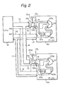
- FIG. 2 illustrates an example of a computer system which uses semiconductor IC devices according to a first embodiment of the present invention.
- the computer system of Fig. 2 is composed of a CPU 10, bus buffers lla and llb, peripheral LSI's 12a and 12b, address setting circuits 13a and 13b, and so on.
- the bus buffers lla and llb are inserted midway of a bus line 14, for example, an address bus, which connects the CPU 10 and-the peripheral LSI's 12a and 12b.
- the CPU 10 is connected to the semiconductor IC devices, i.e., peripheral LSI's 12a and 12b, via a data bus 17, an I/O selecting line 15, and a reset signal line 16 in addition to the bus line 14.
- peripheral LSI's 12a and 12b comprise input buffers 121a and 121b, address memories 122a and 122b, and comparators 123a and 123b which are connected to the bus line 14, respectively.
- the address setting circuit 13a comprises one or more resistors 131a and/or one or more resistors 132a.
- the resistors 131a are connected between a power source V and one or more signal lines corresponding to predetermined bits of the bus line 14 having a plurality of signal lines.
- the resistors 132a are connected between one or more signal lines corresponding to the other bits of the bus line 14 and the ground. Therefore, these resistors of the address setting circuit 13a serve to add a high level voltage or a low level voltage to the signal lines corresponding to predetermined bits, thereby inputting a predetermined address signal to the peripheral LSI 12a.
- the address setting circuit 13b also comprises one or more resistors 131b and/or one or more resistors 132b.
- the resistors 131b are connected between a power source V cc and one or more signal linescorresponding to predetermined bits of the bus line 14.
- the resistors 132b are connected between one or more signal lines corresponding to the other bits of the bus line 14 and the ground, thereby inputting a predetermined address signal to the peripheral LSI 12b.
- the reset signal line 16 connected to a reset terminal RST of the CPU 10 is rendered to an active status, for example, a high potential level, when the initial setting of the computer system is effected, for example, when the power source to the computer system is turned on.
- the bus buffers lla and llb enter a turned-off state, and the CPU 10 and peripheral portions such as the peripheral LSI's 12a and 12b are separated.
- address signals are transmitted to the peripheral LSI's 12a and 12b from the address setting circuits 13a and 13b, respectively which are connected to the bus line 14 on the side of the peripheral LSI's 12a and 12b. That is, among the signal lines of the bus line 14 corresponding to each bit of the address signal, the signal lines pulled up to the power source V cc via the resistors 131a and 131b become high and the signal lines connected to the ground via the resistors 132a and 132b become low.
- the address signals applied to the bus line 14 in this manner are transmitted to the address memories 122a and 122b via the internal buffers 121a and 121b of the peripheral LSI's 12a and 12b and stored therein as the logical numbers of the peripheral LSI's 12a and 12b, respectively.
- the logical numbers are written into the address memories and 122a and 122b by rendering them to a write-in status by the reset signal supplied via the reset signal line 16.
- the CPU 10 accesses one of the peripheral LSI 's after the logical number, i.e., the address of each peripheral LSI, is stored in the above-mentioned manner, an address of a peripheral LSI is transmitted from the CPU 10 via the bus line 14 and the potential of the I/O selecting line 15 is rendered high, so that the I/O selecting signal becomes active.
- the comparator 123a or 123b is enabled and compares the address data input from the CPU 10 and its own logical number read out from the address memory 122a or 122b.
- the CPU 10 informs the comparators 123a and 123b that the data on the bus line 14 at present is the address data supplied to the peripheral LSI's, by rendering the potential of the I/O line 15 high.
- the comparator 123a If, for example, in the peripheral LSI 12a, the aforementioned two data coincide with each other when the comparison by the comparator 123a is effected, the comparator 123a outputs a coincidence signal, i.e., a chip select signal CS which is supplied to the chip select terminal of a peripheral circuit which is provided in the peripheral LSI (not shown).
- a coincidence signal i.e., a chip select signal CS which is supplied to the chip select terminal of a peripheral circuit which is provided in the peripheral LSI (not shown).
- Figure 3 illustrates another computer system which uses semiconductor IC devices according to an embodiment of the present invention. Parts similar to those in Fig. 2 are given the same reference numerals.
- the difference between the systems of Figs. 2 and 3 is that address setting circuits 18a and 18b are used instead of circuits 13a and 13b.
- the address setting circuit 18a comprises resistors 181a through 184a and switches 185a through 188a.
- the address setting circuit 18b comprises resistors 181b through 184b and switches 185b through 188a.
- the bus line 14 thus comprises, for example, four signal lines 14-1, 14-2, 14-3, and 14-4.
- Each of bus buffers lla and llb similarly comprises four buffer amplifiers 19 connected to the signal lines 14-1, 14-2, 14-3, and 14-4, respectively, each of which is activated depending on the reset signal sent from the CPU 10 via the reset signal line 16.
- the logical number of each of the peripheral LSI's 12a and 12b is changeable by the switches 185a through 188a of the address setting circuit 18a or the switches 185b through 188b of the address setting circuit 18b.
- the reset signal is active at the initial setting status, all the buffer amplifiers 19 in each of the address setting circuits lla and llb are turned off.
- the address setting circuits 18a and 18b transmit address signals to the peripheral LSI's 12a and 12b.
- the contents of the address signals, i.e., the logical numbers of the peripheral LSI's 12a and 12b, are determined by the condition of the switches 185a through 188a and the switches 185b through 188b.
- the semiconductor IC device is an LSI comprising an input buffer, an address memory, a comparator, a flip-flop, inverters, anu a data buffer.
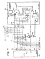
- FIG. 4 illustrates an example of a computer system which uses semiconductor IC devices according to this second embodiment of the present invention.
- the computer system of Fig. 4 comprises a CPU 20, a bus buffer 21, a peripheral LSI 22, an address setting circuit 23, an OR gate 25, and an AND gate 26.
- a common bus line 24 is used as an address bus and a data bus in a time division manner depending on the potential level of a bus switching signal AD/DT.
- the bus line 24 comprises, for example, four signal lines 24-1, 24-2, 24-3 and 24-4 which connect the CPU 20 and the peripheral LSI 22 via the bus buffer 21.
- FIG. 4 only one peripheral LSI 22, one bus buffer 21, and so on are illustrated. However, in practice, a plurality of peripheral LSI's and so on can be connected to the CPU 20.
- the bus buffer 21 comprises dual-direction three--state buffer circuits which are controlled by a direction signal DR and an ON/OFF signal.
- the peripheral LSI 22 comprises an input buffer 221, an address memory 222, a comparator 223, the same as in the first embodiment, and further comprises a flip-flop 224, inverters 225 and 226, and a data buffer 227 inserted between the bus line 24 and internal circuits (not shown) of the peripheral LSI 22.
- the address setting circuit 23 is the same as that of Fig. 3.
- a reset signal on a reset signal line 27 connected to the reset terminal RST of the CPU 20 is rendered to, for example, high when the initial setting of the computer system is effected.
- the reset signal is supplied to the ON/OFF terminal of the bus buffer 21 via the OR gate 25, whereby the bus buffer 21 enters a turned-off state and the CPU 20 and the peripheral LSI 22 are separated. Therefore, an address signal, i.e., a logical number, is transmitted from the address setting circuit 23 to the address memory 222 and stored therein in a manner similar to the computer system of Fig. 3.
- FIGS 5A and 5B illustrate signals of each portion in the system of Fig. 4 in the cases where the CPU 20 accesses the peripheral LSI 22 when it is and is not selected, respectively.
- the CPU 20 accesses one of the peripheral LSI's connected thereto after the logical numbers are preset therein in the above-mentioned manner, the CPU 20 renders the bus switching signal AD/DT to low and sends out an address of a peripheral LSI on a CPU bus, i.e, on the portion of the bus line connected to the CPU 20. Since the output signal of the AND gate is low and the ON/OFF signal is low, the bus buffer 21 enters a turned-on state.
- the direction signal DR is rendered, for example, high and the three-state buffer circuits in the bus buffer 21 are activated, so that signals are transmitted from the side of the CPU 20 to the side of the peripheral LSI 22. Therefore, the address signal sent from the CPU 20 is input to the comparator 223 and compared with the logical number stored in the address memory 222.
- the comparator 223 renders the chip select signal CS to high, so that the peripheral LSI 22 is selected. Therefore, the inverted chip select signal CS, i.e., the output signal of the inverter 225 becomes low, as illustrated in Fig. 5A.
- the CPU 20 renders the bus switching signal AD/DT high and sends out or receives data via the bus line 24. Since the inverted chip select signal CS supplied to a clear terminal CLR of the flip-flop 224 is low, the output signal (Q) of the flip-flop 224 is low. Therefore, the output signal of the AND gate 26 and the output signal of the OR gate 25 are low, and the ON/OFF signal is retained in a low potential level.
- the comparator 223 renders the chip select signal CS to low, so that the peripheral LSI 22 is not selected.
- the CPU 20 renders the bus switching signal AD/DT to high
- the output of the flip-flop 224 becomes high and the output signal of the AND gate 26 becomes high. Therefore, the ON/OFF signal becomes high and the bus buffer 21 are turned off, so that the data sent from the CPU 20 is not transmitted to the peripheral LSI 22, as illustrated in Fig. 5B.
- the interface circuits between a central processing unit and peripheral circuits can be simplified. Since the number of peripheral LSI's is usually not large, it is not necessary to connect signal lines corresponding to all bits of a bus line which connects the central processing unit and the peripheral LSI's to the peripheral LSI's. It is only necessary to connect the signal lines of the bit numbers, e.g., four, determined by the number of the peripheral LSI to the peripheral LSI. Therefore, it is possible to decrease the number of connections between the CPU and the peripheral circuits.
Landscapes
- Engineering & Computer Science (AREA)
- Theoretical Computer Science (AREA)
- Physics & Mathematics (AREA)
- General Engineering & Computer Science (AREA)
- General Physics & Mathematics (AREA)
- Multi Processors (AREA)
- Memory System (AREA)
- Microcomputers (AREA)
- Semiconductor Integrated Circuits (AREA)
Applications Claiming Priority (2)
| Application Number | Priority Date | Filing Date | Title |
|---|---|---|---|
| JP57169542A JPS5960786A (ja) | 1982-09-30 | 1982-09-30 | 半導体集積回路 |
| JP169542/82 | 1982-09-30 |
Publications (3)
| Publication Number | Publication Date |
|---|---|
| EP0105755A2 true EP0105755A2 (de) | 1984-04-18 |
| EP0105755A3 EP0105755A3 (en) | 1986-10-08 |
| EP0105755B1 EP0105755B1 (de) | 1990-04-18 |
Family
ID=15888411
Family Applications (1)
| Application Number | Title | Priority Date | Filing Date |
|---|---|---|---|
| EP83305969A Expired EP0105755B1 (de) | 1982-09-30 | 1983-09-30 | Selektiver Zugriff in Datenverarbeitungsanlagen |
Country Status (4)
| Country | Link |
|---|---|
| US (1) | US4707802A (de) |
| EP (1) | EP0105755B1 (de) |
| JP (1) | JPS5960786A (de) |
| DE (1) | DE3381477D1 (de) |
Cited By (3)
| Publication number | Priority date | Publication date | Assignee | Title |
|---|---|---|---|---|
| EP0209923A1 (de) * | 1985-06-06 | 1987-01-28 | Koninklijke Philips Electronics N.V. | Anordnung zur Identifizierung von peripheren Geräten, die wahlweise mit Hilfe von lokalen Kopplungseinheiten an verschiedenen geographischen Orten mit einem Nachrichtennetz verbunden werden können |
| US4959836A (en) * | 1987-12-09 | 1990-09-25 | Siemens Transmission Systems, Inc. | Register robustness improvement circuit and method |
| FR2675605A1 (fr) * | 1991-04-19 | 1992-10-23 | Alcatel Business Systems | Procede et dispositif d'adressage de peripheriques pour le partage d'un canal de transmission de donnees entre les peripheriques. |
Families Citing this family (6)
| Publication number | Priority date | Publication date | Assignee | Title |
|---|---|---|---|---|
| US5202968A (en) * | 1988-03-30 | 1993-04-13 | Kabushiki Kaisha Toshiba | Expansion system |
| JPH0628243A (ja) * | 1992-07-09 | 1994-02-04 | Fujitsu Ltd | 半導体集積回路 |
| JPH06342398A (ja) * | 1993-06-01 | 1994-12-13 | Fuoratsukusu:Kk | 入出力用メモリ空間の割り付け方法及びその装置 |
| US6078318A (en) * | 1995-04-27 | 2000-06-20 | Canon Kabushiki Kaisha | Data transfer method, display driving circuit using the method, and image display apparatus |
| WO2010016817A1 (en) * | 2008-08-08 | 2010-02-11 | Hewlett-Packard Development Company, L.P. | Independently controllable and reconfigurable virtual memory devices in memory modules that are pin-compatible with standard memory modules |
| ES2395107B1 (es) * | 2011-07-08 | 2013-10-09 | Caf Power & Automation, S.L.U. | Módulo de entradas y salidas para sistemas de monitorización y control de vehículos ferroviarios. |
Family Cites Families (8)
| Publication number | Priority date | Publication date | Assignee | Title |
|---|---|---|---|---|
| DE2364254B2 (de) * | 1973-12-22 | 1976-03-18 | Schaltungsanordnung fuer datenverarbeitende geraete | |
| JPS50154033A (de) * | 1974-05-31 | 1975-12-11 | ||
| US4220991A (en) * | 1977-10-08 | 1980-09-02 | Tokyo Electric Co., Ltd. | Electronic cash register with removable memory packs for cashier identification |
| US4296467A (en) * | 1978-07-03 | 1981-10-20 | Honeywell Information Systems Inc. | Rotating chip selection technique and apparatus |
| GB2087607B (en) * | 1980-11-06 | 1984-10-24 | British Gas Corp | Computer-based control system |
| DE3104941A1 (de) * | 1981-02-11 | 1982-08-26 | Siemens AG, 1000 Berlin und 8000 München | Mikrorechnersystem zum raschen auffinden von kennzeichenbloecken |
| GB2103397A (en) * | 1981-07-31 | 1983-02-16 | Philips Electronic Associated | Digital data aparatus with memory selection |
| FR2520896B1 (fr) * | 1982-02-01 | 1987-06-05 | Merlin Gerin | Dispositif d'adressage des cartes d'un automate programmable pour la securite des echanges sur le bus |
-
1982
- 1982-09-30 JP JP57169542A patent/JPS5960786A/ja active Pending
-
1983
- 1983-09-20 US US06/534,135 patent/US4707802A/en not_active Expired - Fee Related
- 1983-09-30 DE DE8383305969T patent/DE3381477D1/de not_active Expired - Lifetime
- 1983-09-30 EP EP83305969A patent/EP0105755B1/de not_active Expired
Cited By (4)
| Publication number | Priority date | Publication date | Assignee | Title |
|---|---|---|---|---|
| EP0209923A1 (de) * | 1985-06-06 | 1987-01-28 | Koninklijke Philips Electronics N.V. | Anordnung zur Identifizierung von peripheren Geräten, die wahlweise mit Hilfe von lokalen Kopplungseinheiten an verschiedenen geographischen Orten mit einem Nachrichtennetz verbunden werden können |
| US4959836A (en) * | 1987-12-09 | 1990-09-25 | Siemens Transmission Systems, Inc. | Register robustness improvement circuit and method |
| FR2675605A1 (fr) * | 1991-04-19 | 1992-10-23 | Alcatel Business Systems | Procede et dispositif d'adressage de peripheriques pour le partage d'un canal de transmission de donnees entre les peripheriques. |
| EP0510482A1 (de) * | 1991-04-19 | 1992-10-28 | Alcatel Business Systems | Adressierungsverfahren und Einrichtung zur gemeinsamen Benutzung eines Übertragungskanals für Peripheriegeräte |
Also Published As
| Publication number | Publication date |
|---|---|
| DE3381477D1 (de) | 1990-05-23 |
| US4707802A (en) | 1987-11-17 |
| EP0105755A3 (en) | 1986-10-08 |
| EP0105755B1 (de) | 1990-04-18 |
| JPS5960786A (ja) | 1984-04-06 |
Similar Documents
| Publication | Publication Date | Title |
|---|---|---|
| US4694394A (en) | Microprocessor system having a multiplexed address/data bus which communicates with a plurality of memory and input/output devices including TTL output gates | |
| US4571676A (en) | Memory module selection and reconfiguration apparatus in a data processing system | |
| US4158227A (en) | Paged memory mapping with elimination of recurrent decoding | |
| US4156932A (en) | Programmable communications controller | |
| US4964038A (en) | Data processing system having automatic address allocation arrangements for addressing interface cards | |
| US5881281A (en) | Method and apparatus for automatically loading configuration data on reset into a host adapter integrated circuit | |
| EP0076629B1 (de) | Rekonfigurierbares Speichersystem | |
| US4511959A (en) | Decentralized arbitration device for several processing units of a multiprocessor system | |
| EP0111840A2 (de) | Zugriffsteuerungsverfahren für Multiprozessorsysteme | |
| EP0156316A2 (de) | Speicheranordnung mit Datenzugriffsteuerung | |
| JPH039492B2 (de) | ||
| GB1580313A (en) | Rom memory systems | |
| US5119336A (en) | Memory write protection circuit | |
| US6483183B1 (en) | Integrated circuit (IC) package with a microcontroller having an n-bit bus and up to n-pins coupled to the microcontroller | |
| US5548777A (en) | Interface control system for a CD-ROM driver by memory mapped I/O method having a predetermined base address using an ISA BUS standard | |
| US4183086A (en) | Computer system having individual computers with data filters | |
| US5025415A (en) | Memory card | |
| EP0105755B1 (de) | Selektiver Zugriff in Datenverarbeitungsanlagen | |
| US5375218A (en) | DMA channel control apparatus capable of assigning independent DMA transfer control line to respective expansion slots | |
| US5243701A (en) | Method of and system for processing data having bit length variable with modes of operation | |
| US4040029A (en) | Memory system with reduced block decoding | |
| EP0800139A2 (de) | Programmierbares Lese/-Schreibzugriffsignal und Verfahren | |
| EP0265575A1 (de) | Datenverarbeitungsanordnung mit Vorrichtungen zur automatischen Adresszuordnung zur Adressierung von Schnittstellenmodulen | |
| US5426432A (en) | IC card | |
| US5630167A (en) | Electronic apparatus having a plurality of connectors each connecting one of a plurality of kinds of cards |
Legal Events
| Date | Code | Title | Description |
|---|---|---|---|
| PUAI | Public reference made under article 153(3) epc to a published international application that has entered the european phase |
Free format text: ORIGINAL CODE: 0009012 |
|
| AK | Designated contracting states |
Designated state(s): DE FR GB |
|
| PUAL | Search report despatched |
Free format text: ORIGINAL CODE: 0009013 |
|
| AK | Designated contracting states |
Kind code of ref document: A3 Designated state(s): DE FR GB |
|
| 17P | Request for examination filed |
Effective date: 19870313 |
|
| 17Q | First examination report despatched |
Effective date: 19880928 |
|
| GRAA | (expected) grant |
Free format text: ORIGINAL CODE: 0009210 |
|
| AK | Designated contracting states |
Kind code of ref document: B1 Designated state(s): DE FR GB |
|
| REF | Corresponds to: |
Ref document number: 3381477 Country of ref document: DE Date of ref document: 19900523 |
|
| ET | Fr: translation filed | ||
| PLBE | No opposition filed within time limit |
Free format text: ORIGINAL CODE: 0009261 |
|
| STAA | Information on the status of an ep patent application or granted ep patent |
Free format text: STATUS: NO OPPOSITION FILED WITHIN TIME LIMIT |
|
| 26N | No opposition filed | ||
| PGFP | Annual fee paid to national office [announced via postgrant information from national office to epo] |
Ref country code: GB Payment date: 19920707 Year of fee payment: 10 |
|
| PGFP | Annual fee paid to national office [announced via postgrant information from national office to epo] |
Ref country code: FR Payment date: 19920929 Year of fee payment: 10 |
|
| PGFP | Annual fee paid to national office [announced via postgrant information from national office to epo] |
Ref country code: DE Payment date: 19921125 Year of fee payment: 10 |
|
| PG25 | Lapsed in a contracting state [announced via postgrant information from national office to epo] |
Ref country code: GB Effective date: 19930930 |
|
| GBPC | Gb: european patent ceased through non-payment of renewal fee |
Effective date: 19930930 |
|
| PG25 | Lapsed in a contracting state [announced via postgrant information from national office to epo] |
Ref country code: FR Free format text: LAPSE BECAUSE OF NON-PAYMENT OF DUE FEES Effective date: 19940531 |
|
| PG25 | Lapsed in a contracting state [announced via postgrant information from national office to epo] |
Ref country code: DE Effective date: 19940601 |
|
| REG | Reference to a national code |
Ref country code: FR Ref legal event code: ST |