EP0106600A2 - Circuit de contrôle de protection de mémoire - Google Patents
Circuit de contrôle de protection de mémoire Download PDFInfo
- Publication number
- EP0106600A2 EP0106600A2 EP83305875A EP83305875A EP0106600A2 EP 0106600 A2 EP0106600 A2 EP 0106600A2 EP 83305875 A EP83305875 A EP 83305875A EP 83305875 A EP83305875 A EP 83305875A EP 0106600 A2 EP0106600 A2 EP 0106600A2
- Authority
- EP
- European Patent Office
- Prior art keywords
- storage
- key
- circuit
- access
- protection
- Prior art date
- Legal status (The legal status is an assumption and is not a legal conclusion. Google has not performed a legal analysis and makes no representation as to the accuracy of the status listed.)
- Granted
Links
Images

Classifications
-
- G—PHYSICS
- G06—COMPUTING OR CALCULATING; COUNTING
- G06F—ELECTRIC DIGITAL DATA PROCESSING
- G06F13/00—Interconnection of, or transfer of information or other signals between, memories, input/output devices or central processing units
-
- G—PHYSICS
- G06—COMPUTING OR CALCULATING; COUNTING
- G06F—ELECTRIC DIGITAL DATA PROCESSING
- G06F12/00—Accessing, addressing or allocating within memory systems or architectures
- G06F12/14—Protection against unauthorised use of memory or access to memory
-
- G—PHYSICS
- G06—COMPUTING OR CALCULATING; COUNTING
- G06F—ELECTRIC DIGITAL DATA PROCESSING
- G06F12/00—Accessing, addressing or allocating within memory systems or architectures
- G06F12/14—Protection against unauthorised use of memory or access to memory
- G06F12/1458—Protection against unauthorised use of memory or access to memory by checking the subject access rights
- G06F12/1466—Key-lock mechanism
Definitions
- the present invention relates to a method for checking storage protection in a system providing a storage-protection key in each unit area.
- a previous method for checking storage--protection is given in "IBM - System/370 Principles of Operation" (GA 22-7000-6 File No. 370-01). That is, a main storage device is divided into a plurality of pages as unitsof storage protection, for example, into two-kilobyte blocks, and storage keys having eight bits are written into a key storage.
- the storage keys have the following construction:
- A denotes an access control bit
- F denotes a read protection bit
- R denotes a reference bit
- C denotes a change bit
- S denotes a write protection bit.
- a central processing unit or a channel provides a protection key.
- the central processing unit provides a protection key in program--status words (PSW) and a storage key in translation look aside buffers (TLB).
- PSW program--status words
- TLB translation look aside buffers
- the channel reads the channel-address words (CAW) and maintains-the protection key written into the CAW.
- CAW channel-address words
- An / of the present invention can provide a method for checking memory protection by which memory protection of an access request to the main storage can be rapidly checked.
- a storage-protection-check circuit comprising: an access control circuit which receives an access request from a channel; a main storage control circuit and a storage-protection key control circuit which are controlled by the access control circuit; a main storage which is controlled by the main storage control circuit; a key storage which is controlled by the storage-protection key control circuit; and a storage-protection-check circuit which receives an access request key from the channel, a key storage check signal from the storage-protection key control circuit, and a storage key from the key storage and outputs a main storage access admission signal to the access control circuit, the storage-protection-check circuit comprising a zero check circuit which receives the access request, a coincidence check circuit which receives the access request and the storage key from the key storage, a first AND circuit which receives'the output of the zero check circuit and a key storage access request from the access control circuit, a second AND circuit which receives via a NOT circuit the output of the
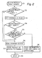
- Figure 1 shows a conventional storage-protection--check circuit.
- 1 denotes an access control circuit
- 2 denotes a main storage control circuit
- 3 denotes a storage-protection key control circuit
- 4 denotes a storage-protection-check circuit
- 5 denotes a main storage
- 6 denotes a key storage
- 10 denotes an access request
- 11 denotes an access request key
- 12 denotes a main storage access request
- 13 denotes a key storage access request
- 20 denotes a line which transmits main storage access information
- 30 denotes a line which transmits key storage access information
- 31 denotes a key storage check signal
- 40 denotes a main storage access admission signal
- 42 denotes a zero check signal
- 43 denotes a coincidence signal
- Z denotes a zero check circuit
- M denotes a coincidence check circuit
- O denotes an OR circuit
- A denotes an AND circuit.
- the access control circuit 1 analyzes the access request and controls the main storage control circuit 2 and the storage-protection key control circuit 3 in accordance with the result of analysis.
- the main storage control circuit 2 controls the main storage 5, and the storage-protection key control circuit 3 controls the key storage 6.
- the storage-protection--check circuit 4 includes the zero check circuit Z, the coincidence check circuit M, the OR circuit O, and the AND circuit A.
- the zero check circuit Z determines whether or not the access request key 11 is zero
- the coincidence check circuit M determines whether or not the access request key 11 and the storage key 60 read from the key storage 6 are coincident.
- the access request key 11 includes both protection key information and read/write information.
- the channel accesses the main storage via a block boundary of pages
- the channel sends an access request requiring a key check to the access control circuit 1.
- the central processing unit since the central processing unit reads the storage key into the TLB before receiving this access request, the central processing unit checks whether a request for main storage access is possible or not.
- the access control circuit 1 receives the access request having a key check
- the access control circuit 1 sends the key storage access request 13 to the storage-protection key control circuit 3.
- the storage-projection key control circuit 3 receives the key storage access request 13, it sends the key storage access information 30 to the key storage 6.
- the key storage access information 30 includes a read/write signal indicating read or write and key storage address information. In this case, the read/write signal indicates read.
- the storage key 60 which is read out of the key storage 6 is sent to the coincidence check circuit M in the storage-protection-check circuit 4. If the zero check signal 42 or the coincidence signal 43 is logic "1" when the storage-protection key control circuit 3 sends the key storage check signal 31, the value of which is logic "1", the main storage access admission signal 40 becomes logic "1". When the main storage access admission signal 40 becomes logic "1", the access control circuit 1 sends the main storage access request 12 to the main storage control circuit 2. When the main strage control circuit 2 receives the main storage access request 12, the main stroage control circuit 2 sends the main storage access information 20 to the main storage 5. The main storage 5 effects read/write in accordance with the main storage access information 20.
- Figure 2 is a flow chart illustrating the operation of the circuit shown in Fig. 1.
- it is checked whether or not an access request from the channel (block 51) has a key check (block 52). If it has a key check the key storage is read (block 53), and it is checked in block 54 whether or not the access request key is zero. If the access request key is not zero, it is checked in block 55 whether or not the read (that is, the storage key read from the key storage) key/is coincident with the access request. If the read key is coincident with the access request, the main storage is accessed in block 56 and the result of access is sent to the channel in block 57. If the read key is not coincident with the access request, a key check is impossible.
- the main storage access admission signal may be logic "1" when the storage check signal becomes logic "1". In such a conventional system, the time during which the next key storage access request is awaited becomes long and the key storage cannot be efficiently accessed.
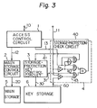
- FIG. 3 illustrates one embodiment of the present invention.
- a 1 to A 3 denote AND circuit
- N denotes a NOT circuit
- 41 denotes a key storage access admission signal.
- the other elements in Fig. 3 are the same as the elements in Fig. 1 and are represented by the same reference numerals as in Fig. 1.
- the storage-protection-check circuit 4 shown in Fig. 3 includes a zero check circuit 2, a coincidence check circuit M, the NOT circuit N, the AND circuits A 1 to A 3 , and an OR circuit 0.
- the AND circuit A 1 receives a zero check signal 42 and a key storage access request 13, and the AND circuit A3 receives a coincidence.signal'43 and a key storage check signal 31.
- the outputs of the AND circuits A 1 and A3 are supplied to the input of the OR circuit 0, and the output of the OR circuit 0 is used as a main storage access admission signal 40.
- the AND circuit A 2 receives the key storage access request 13 and an inverted signal of the zero check signal 42. The output of the AND circuit A 2 becomes the key storage access admission signal 41.
- the channel accesses, via the block boundary, a main storage 5, the channel sends an access request 10 having a key check and an access request key 11 to an access control circuit 1.
- the access control circuit 1 receives the access request 10 having a key check
- the access control circuit 1 sends the key storage access request 13 to the AND circuits A 1 and A 2 .
- the access request key 11 is supplied to the zero check circuit Z. If the zero check signal 42 is logic "1" when the key storage access request 13 is sent to the AND circuits A 1 and A 2 , the main storage access admission signal 40 becomes logic "1".
- the access control circuit 1 controls so as to carry out main storage access.
- the key storage access admission signal 41 is sent to a storage--protection key control circuit 3.
- the storage--protection key control circuit 3 receives the key storage access admission signal 41, the circuit 3 sends key storage access information 30 to a key storage 6.
- a storage key 60 which is read out of the key storage 6, is supplied to the coincidence check circuit M in the storage-protection-check circuit 4.
- the coincidence signal 43 is sent via the AND circuit A3 and the OR circuit 0 to the access control circuit 1 so that the main storage access admission signal 40 is sent to the access control circuit 1.
- the access control circuit 1 controls so as to carry out main storage access.
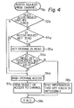
- Figure 4 is a flow chart illustrating the operation of the circuit shown in Fig. 3.
- blocks 51a to 59a correspond to blocks 51 to 59 in Fig. 2.
- Fig. 4 differs from that of Fig. 2 in that the order of blocks 53a and 54a is reversed. That is, the value of the access request key having an access request is checked in block 54a, and when the value of the access request key is zero, the main storage is accessed in block 56a.
- a circuit for checking protection includes a storage key corresponding to the unit area of a storage region and being stored in a key storage. The value of the access request key of an access request corresponding to the storage region is checked. When the access request key has a specified value, the storage region is accessed without reading the storage key out of the key storage.
- the main storage can be accessed without accessing the key storage, Therefore, accessing of the key storage can be efficiently carried out.
Landscapes
- Engineering & Computer Science (AREA)
- Theoretical Computer Science (AREA)
- Physics & Mathematics (AREA)
- General Engineering & Computer Science (AREA)
- General Physics & Mathematics (AREA)
- Computer Security & Cryptography (AREA)
- Storage Device Security (AREA)
Applications Claiming Priority (2)
| Application Number | Priority Date | Filing Date | Title |
|---|---|---|---|
| JP57170080A JPS5958700A (ja) | 1982-09-29 | 1982-09-29 | 記憶保護判定方式 |
| JP170080/82 | 1982-09-29 |
Publications (3)
| Publication Number | Publication Date |
|---|---|
| EP0106600A2 true EP0106600A2 (fr) | 1984-04-25 |
| EP0106600A3 EP0106600A3 (en) | 1987-01-21 |
| EP0106600B1 EP0106600B1 (fr) | 1989-12-27 |
Family
ID=15898265
Family Applications (1)
| Application Number | Title | Priority Date | Filing Date |
|---|---|---|---|
| EP83305875A Expired EP0106600B1 (fr) | 1982-09-29 | 1983-09-29 | Circuit de contrôle de protection de mémoire |
Country Status (9)
| Country | Link |
|---|---|
| US (1) | US4954982A (fr) |
| EP (1) | EP0106600B1 (fr) |
| JP (1) | JPS5958700A (fr) |
| KR (1) | KR880000360B1 (fr) |
| AU (1) | AU545373B2 (fr) |
| BR (1) | BR8305341A (fr) |
| CA (1) | CA1208803A (fr) |
| DE (1) | DE3381025D1 (fr) |
| ES (1) | ES8502275A1 (fr) |
Cited By (1)
| Publication number | Priority date | Publication date | Assignee | Title |
|---|---|---|---|---|
| US8536377B2 (en) | 2008-11-05 | 2013-09-17 | Basf Se | Method for producing N,N-substituted-3-aminopropan-1-ols |
Families Citing this family (27)
| Publication number | Priority date | Publication date | Assignee | Title |
|---|---|---|---|---|
| US5297268A (en) * | 1988-06-03 | 1994-03-22 | Dallas Semiconductor Corporation | ID protected memory with a readable/writable ID template |
| DE68928937T2 (de) * | 1988-12-27 | 1999-07-01 | Fujitsu Ltd., Kawasaki, Kanagawa | Steuerungssystem und -verfahren zum Instruction Fetch |
| DE3901457A1 (de) * | 1989-01-19 | 1990-08-02 | Strahlen Umweltforsch Gmbh | Verfahren zur adressbereichsueberwachung bei datenverarbeitungsgeraeten in echtzeit |
| US5335334A (en) * | 1990-08-31 | 1994-08-02 | Hitachi, Ltd. | Data processing apparatus having a real memory region with a corresponding fixed memory protection key value and method for allocating memories therefor |
| US5163096A (en) * | 1991-06-06 | 1992-11-10 | International Business Machines Corporation | Storage protection utilizing public storage key control |
| JP3006730B2 (ja) * | 1991-08-13 | 2000-02-07 | 富士ゼロックス株式会社 | 共同作業用情報処理装置及び共同作業用情報処理方法 |
| JP2788836B2 (ja) * | 1992-05-15 | 1998-08-20 | インターナショナル・ビジネス・マシーンズ・コーポレイション | ディジタルコンピュータシステム |
| US5475829A (en) * | 1993-03-22 | 1995-12-12 | Compaq Computer Corp. | Computer system which overrides write protection status during execution in system management mode |
| US5802397A (en) * | 1996-05-23 | 1998-09-01 | International Business Machines Corporation | System for storage protection from unintended I/O access using I/O protection key by providing no control by I/O key entries over access by CP entity |
| US5724551A (en) * | 1996-05-23 | 1998-03-03 | International Business Machines Corporation | Method for managing I/O buffers in shared storage by structuring buffer table having entries include storage keys for controlling accesses to the buffers |
| US5787309A (en) * | 1996-05-23 | 1998-07-28 | International Business Machines Corporation | Apparatus for protecting storage blocks from being accessed by unwanted I/O programs using I/O program keys and I/O storage keys having M number of bits |
| US5809546A (en) * | 1996-05-23 | 1998-09-15 | International Business Machines Corporation | Method for managing I/O buffers in shared storage by structuring buffer table having entries including storage keys for controlling accesses to the buffers |
| US5900019A (en) * | 1996-05-23 | 1999-05-04 | International Business Machines Corporation | Apparatus for protecting memory storage blocks from I/O accesses |
| US6324537B1 (en) * | 1999-09-30 | 2001-11-27 | M-Systems Flash Disk Pioneers Ltd. | Device, system and method for data access control |
| US6807620B1 (en) * | 2000-02-11 | 2004-10-19 | Sony Computer Entertainment Inc. | Game system with graphics processor |
| IL148834A (en) | 2000-09-10 | 2007-03-08 | Sandisk Il Ltd | Removable, active, personal storage device, system and method |
| US6526491B2 (en) * | 2001-03-22 | 2003-02-25 | Sony Corporation Entertainment Inc. | Memory protection system and method for computer architecture for broadband networks |
| US7093104B2 (en) * | 2001-03-22 | 2006-08-15 | Sony Computer Entertainment Inc. | Processing modules for computer architecture for broadband networks |
| US7233998B2 (en) * | 2001-03-22 | 2007-06-19 | Sony Computer Entertainment Inc. | Computer architecture and software cells for broadband networks |
| US6809734B2 (en) | 2001-03-22 | 2004-10-26 | Sony Computer Entertainment Inc. | Resource dedication system and method for a computer architecture for broadband networks |
| US7231500B2 (en) * | 2001-03-22 | 2007-06-12 | Sony Computer Entertainment Inc. | External data interface in a computer architecture for broadband networks |
| US7516334B2 (en) | 2001-03-22 | 2009-04-07 | Sony Computer Entertainment Inc. | Power management for processing modules |
| US6826662B2 (en) | 2001-03-22 | 2004-11-30 | Sony Computer Entertainment Inc. | System and method for data synchronization for a computer architecture for broadband networks |
| US7024519B2 (en) * | 2002-05-06 | 2006-04-04 | Sony Computer Entertainment Inc. | Methods and apparatus for controlling hierarchical cache memory |
| US8224639B2 (en) | 2004-03-29 | 2012-07-17 | Sony Computer Entertainment Inc. | Methods and apparatus for achieving thermal management using processing task scheduling |
| US8265270B2 (en) * | 2007-12-05 | 2012-09-11 | Microsoft Corporation | Utilizing cryptographic keys and online services to secure devices |
| GB2578924B (en) * | 2018-11-14 | 2021-09-29 | Advanced Risc Mach Ltd | An apparatus and method for controlling memory accesses |
Family Cites Families (17)
| Publication number | Priority date | Publication date | Assignee | Title |
|---|---|---|---|---|
| US3284776A (en) * | 1961-06-08 | 1966-11-08 | Decca Ltd | Data processing apparatus |
| US3328765A (en) * | 1963-12-31 | 1967-06-27 | Ibm | Memory protection system |
| US3328768A (en) * | 1964-04-06 | 1967-06-27 | Ibm | Storage protection systems |
| US3377626A (en) * | 1966-04-01 | 1968-04-16 | Robert E. Smith | Insulated goggles |
| US3576544A (en) * | 1968-10-18 | 1971-04-27 | Ibm | Storage protection system |
| DE2010640A1 (de) * | 1969-05-19 | 1970-11-26 | VEB Kombinat Robotron, χ 8l42 Radeberg | Patentwesen, Ost-Berlin WPI3989O Schaltungsanordnung zur Durchführung des Speicherschutzes in Verbindung mit Kanalsteuereinheiten |
| DE2047287A1 (de) * | 1969-10-27 | 1972-02-03 | Robotron Veb K | Verfahren und Schaltungsanordnung zur Durchfuhrung des Schutzes von Speicher platzen |
| US3825903A (en) * | 1973-04-30 | 1974-07-23 | Ibm | Automatic switching of storage protect keys |
| US4135240A (en) * | 1973-07-09 | 1979-01-16 | Bell Telephone Laboratories, Incorporated | Protection of data file contents |
| JPS5247858A (en) * | 1975-10-14 | 1977-04-16 | Kobe Steel Ltd | Device for coating steel pipe |
| US4038645A (en) * | 1976-04-30 | 1977-07-26 | International Business Machines Corporation | Non-translatable storage protection control system |
| US4035779A (en) * | 1976-04-30 | 1977-07-12 | International Business Machines Corporation | Supervisor address key control system |
| US4037214A (en) * | 1976-04-30 | 1977-07-19 | International Business Machines Corporation | Key register controlled accessing system |
| JPS542026A (en) * | 1977-06-07 | 1979-01-09 | Hitachi Ltd | Memory unit |
| JPS596415B2 (ja) * | 1977-10-28 | 1984-02-10 | 株式会社日立製作所 | 多重情報処理システム |
| US4521846A (en) * | 1981-02-20 | 1985-06-04 | International Business Machines Corporation | Mechanism for accessing multiple virtual address spaces |
| US4472790A (en) * | 1982-02-05 | 1984-09-18 | International Business Machines Corporation | Storage fetch protect override controls |
-
1982
- 1982-09-29 JP JP57170080A patent/JPS5958700A/ja active Granted
-
1983
- 1983-09-14 CA CA000436651A patent/CA1208803A/fr not_active Expired
- 1983-09-14 AU AU19124/83A patent/AU545373B2/en not_active Ceased
- 1983-09-28 KR KR1019830004556A patent/KR880000360B1/ko not_active Expired
- 1983-09-28 BR BR8305341A patent/BR8305341A/pt not_active IP Right Cessation
- 1983-09-28 ES ES526027A patent/ES8502275A1/es not_active Expired
- 1983-09-29 EP EP83305875A patent/EP0106600B1/fr not_active Expired
- 1983-09-29 DE DE8383305875T patent/DE3381025D1/de not_active Expired - Lifetime
-
1989
- 1989-02-24 US US07/315,213 patent/US4954982A/en not_active Expired - Fee Related
Cited By (1)
| Publication number | Priority date | Publication date | Assignee | Title |
|---|---|---|---|---|
| US8536377B2 (en) | 2008-11-05 | 2013-09-17 | Basf Se | Method for producing N,N-substituted-3-aminopropan-1-ols |
Also Published As
| Publication number | Publication date |
|---|---|
| BR8305341A (pt) | 1984-05-08 |
| CA1208803A (fr) | 1986-07-29 |
| US4954982A (en) | 1990-09-04 |
| ES526027A0 (es) | 1984-12-16 |
| KR880000360B1 (ko) | 1988-03-20 |
| AU1912483A (en) | 1984-04-05 |
| JPS6235702B2 (fr) | 1987-08-03 |
| ES8502275A1 (es) | 1984-12-16 |
| AU545373B2 (en) | 1985-07-11 |
| EP0106600B1 (fr) | 1989-12-27 |
| EP0106600A3 (en) | 1987-01-21 |
| KR840006092A (ko) | 1984-11-21 |
| JPS5958700A (ja) | 1984-04-04 |
| DE3381025D1 (de) | 1990-02-01 |
Similar Documents
| Publication | Publication Date | Title |
|---|---|---|
| EP0106600B1 (fr) | Circuit de contrôle de protection de mémoire | |
| EP0087956B1 (fr) | Système de commande d'unité de mémorisation de clef | |
| US4985828A (en) | Method and apparatus for generating a real address multiple virtual address spaces of a storage | |
| EP0168121B1 (fr) | Méthode et dispositif d'accès à la mémoire dans les systèmes à multi-processeurs | |
| US4701846A (en) | Computer system capable of interruption using special protection code for write interruption region of memory device | |
| US4157586A (en) | Technique for performing partial stores in store-thru memory configuration | |
| CA1226372A (fr) | Systeme de controle de traduction d'adresses | |
| US4115855A (en) | Buffer memory control device having priority control units for priority processing set blocks and unit blocks in a buffer memory | |
| US5119336A (en) | Memory write protection circuit | |
| EP0260433B1 (fr) | Procédé de commande d'espaces d'adressage multiples | |
| US5548777A (en) | Interface control system for a CD-ROM driver by memory mapped I/O method having a predetermined base address using an ISA BUS standard | |
| US4803616A (en) | Buffer memory | |
| EP0076097B1 (fr) | Système de commande de pile d'adresses d'origine de table de segment | |
| EP0285309A2 (fr) | Dispositif de protection de mémoire à utilisation dans un calculateur électronique | |
| JPS6161413B2 (fr) | ||
| JPS59157887A (ja) | 情報処理装置 | |
| WO1988009014A2 (fr) | Systeme d'adressage de memoire | |
| EP0358224A2 (fr) | Dispositif de disque à semi-conducteurs utile dans un système de traitement de transaction | |
| US5440696A (en) | Data processing device for reducing the number of internal bus lines | |
| JPS6126700B2 (fr) | ||
| KR0145790B1 (ko) | 전전자 교환기에 있어서 스카시버스가 연결된 보조기억장치에 대한 이중화제어회로 | |
| JPS6165341A (ja) | ハードウエアマツチヤ装置 | |
| JPS58125287A (ja) | 高速緩衝記憶装置 | |
| GB2030333A (en) | Part-word Addressing | |
| JPS6040115B2 (ja) | バブルメモリのバンクスイツチ方式 |
Legal Events
| Date | Code | Title | Description |
|---|---|---|---|
| PUAI | Public reference made under article 153(3) epc to a published international application that has entered the european phase |
Free format text: ORIGINAL CODE: 0009012 |
|
| AK | Designated contracting states |
Designated state(s): DE FR GB |
|
| PUAL | Search report despatched |
Free format text: ORIGINAL CODE: 0009013 |
|
| AK | Designated contracting states |
Kind code of ref document: A3 Designated state(s): DE FR GB |
|
| 17P | Request for examination filed |
Effective date: 19870710 |
|
| 17Q | First examination report despatched |
Effective date: 19880322 |
|
| GRAA | (expected) grant |
Free format text: ORIGINAL CODE: 0009210 |
|
| AK | Designated contracting states |
Kind code of ref document: B1 Designated state(s): DE FR GB |
|
| ET | Fr: translation filed | ||
| REF | Corresponds to: |
Ref document number: 3381025 Country of ref document: DE Date of ref document: 19900201 |
|
| PLBE | No opposition filed within time limit |
Free format text: ORIGINAL CODE: 0009261 |
|
| STAA | Information on the status of an ep patent application or granted ep patent |
Free format text: STATUS: NO OPPOSITION FILED WITHIN TIME LIMIT |
|
| 26N | No opposition filed | ||
| PGFP | Annual fee paid to national office [announced via postgrant information from national office to epo] |
Ref country code: GB Payment date: 19981001 Year of fee payment: 16 |
|
| PGFP | Annual fee paid to national office [announced via postgrant information from national office to epo] |
Ref country code: DE Payment date: 19981005 Year of fee payment: 16 |
|
| PGFP | Annual fee paid to national office [announced via postgrant information from national office to epo] |
Ref country code: FR Payment date: 19990909 Year of fee payment: 17 |
|
| PG25 | Lapsed in a contracting state [announced via postgrant information from national office to epo] |
Ref country code: GB Free format text: LAPSE BECAUSE OF NON-PAYMENT OF DUE FEES Effective date: 19990929 |
|
| GBPC | Gb: european patent ceased through non-payment of renewal fee |
Effective date: 19990929 |
|
| PG25 | Lapsed in a contracting state [announced via postgrant information from national office to epo] |
Ref country code: DE Free format text: LAPSE BECAUSE OF NON-PAYMENT OF DUE FEES Effective date: 20000701 |
|
| PG25 | Lapsed in a contracting state [announced via postgrant information from national office to epo] |
Ref country code: FR Free format text: LAPSE BECAUSE OF NON-PAYMENT OF DUE FEES Effective date: 20010531 |
|
| REG | Reference to a national code |
Ref country code: FR Ref legal event code: ST |