EP0106724A2 - Balistischer bipolarer Transistor mit Heteroübergängen - Google Patents
Balistischer bipolarer Transistor mit Heteroübergängen Download PDFInfo
- Publication number
- EP0106724A2 EP0106724A2 EP83401740A EP83401740A EP0106724A2 EP 0106724 A2 EP0106724 A2 EP 0106724A2 EP 83401740 A EP83401740 A EP 83401740A EP 83401740 A EP83401740 A EP 83401740A EP 0106724 A2 EP0106724 A2 EP 0106724A2
- Authority
- EP
- European Patent Office
- Prior art keywords
- base
- emitter
- electrons
- semiconductor
- interface
- Prior art date
- Legal status (The legal status is an assumption and is not a legal conclusion. Google has not performed a legal analysis and makes no representation as to the accuracy of the status listed.)
- Granted
Links
Images



Classifications
-
- H—ELECTRICITY
- H10—SEMICONDUCTOR DEVICES; ELECTRIC SOLID-STATE DEVICES NOT OTHERWISE PROVIDED FOR
- H10D—INORGANIC ELECTRIC SEMICONDUCTOR DEVICES
- H10D10/00—Bipolar junction transistors [BJT]
- H10D10/80—Heterojunction BJTs
- H10D10/821—Vertical heterojunction BJTs
-
- H—ELECTRICITY
- H10—SEMICONDUCTOR DEVICES; ELECTRIC SOLID-STATE DEVICES NOT OTHERWISE PROVIDED FOR
- H10D—INORGANIC ELECTRIC SEMICONDUCTOR DEVICES
- H10D10/00—Bipolar junction transistors [BJT]
- H10D10/80—Heterojunction BJTs
- H10D10/821—Vertical heterojunction BJTs
- H10D10/881—Resonant tunnelling transistors
Definitions
- the present invention relates generally to three-terminal semiconductor components such as bipolar transistors, permeable base transistors, planar doped barrier transistors, and more particularly to a component in which the emitter-base barrier is made so as to allow a movement of the quasi-ballistic electrons.
- a component is capable of operating at very high speed.
- U.S. Patent 3,209,215 is an older patent which describes hetero-semiconductor components in which a narrow base region is provided, but in which the emitter, base and collector have the same type of conductivity. This patent describes a structure in which tunnel effects occur but no mention is made of the use of a heterojunction triode with a base whose conductivity is opposite to that of the other electrodes.
- U.S. Patent No. 4,286,275 also describes a three-terminal semiconductor component and is directed to an embodiment intended to achieve increased switching speed. This patent recognizes the limitations of movement by diffusion of charge carriers and solves this problem by choosing the height and width of barrier for the emitter (or injection region of the carriers) so that the injection mechanism of predominant current is the tunnel effect.
- U.S. Patent No. 4,173,763 also describes a hetero-junction transistor in which a base thickness of 100 A or less is used to produce a tunnel effect from the emitter to the collector, in order to '' obtain a component operating at high speed.
- An object of the invention is therefore to propose a bipolar semiconductor component with heterojunction, with three terminals and with high operating speed, which avoids the limitations due to the diffusion mechanism.
- Another object of the invention is to provide a heterojunction ballistic bipolar transistor comprising a base region of conductivity opposite to that of the emitter and collector regions and in which the thickness of the base region is of the order the length of the average free path of minority carriers, the carriers being injected by the transmitter to the base region by means of a potential barrier resulting from the heterogeneous nature of the transmitter-base junction.
- Another object of the invention is to provide a high speed heterojunction bipolar transistor in which the limitations due to the diffusion mechanism are eliminated by virtue of an emitter-base interface barrier which serves to accelerate electrons to neighboring energies. of, but less than, the energy of dispersion to the upper energy valleys.
- Another object of the invention is to propose a heterojunction ballistic bipolar transistor comprising an emitter-base barrier which allows a quasi-ballistic movement of the electrons without diffusion.
- the invention relates to a bipolar heterojunction semiconductor component comprising emitter, base and collector regions, the emitter-base junction can be a GaAlAs-GaAs junction, or can be formed from other compounds III. -V.
- the component is formed in such a way that the difference in mobility of the electrons between the emitter and the base creates a potential barrier in the form of a "peak" at the edge of the conduction band. This crest produces a potential drop for the electrons crossing the barrier and it is used to accelerate the electrons to energy levels close to, but lower than, those which cause a diffusion towards the upper valleys (mainly by interaction of polaro-optic phonons).
- ⁇ E TL 0.56 eV.
- the crest of the conduction band at the emitter-base junction is chosen so that its height allows a thermionic emission of electrons above the crest, the electrons being accelerated to kinetic energy in the Beach of ten times the thermal energy.
- This kinetic energy is preferably about ten percent lower than the energy required to transfer the electrons to the upper valley, and thus produces a maximum speed of the electrons and a maximum length for the mean free path (around 0.15 ⁇ m for 0.3 eV).
- the deflection angle range can be small (5-10 °) so that the desired direction for the speed of the electrons is not seriously affected.
- the width, and more generally the shape, of the crest region is chosen to avoid the tunneling effect through the complete barrier, so that the majority of the electrons can be accelerated to energy. appropriate (not lower energy).
- the shape is also adjusted to reduce the quantum reflection of the electrons that are injected; thus, the slope of the ridge should be lower on the side of the transmitter than on the side of the base.
- the thermal injection energy is approximately 0.26 eV. If the interface region between the emitter and the base has a thickness of 100 A for example, the field is equal to 2.6 x 10 5 V / cm, which produces the desired speed of the electrons. Although other III-V semiconductor compounds lead to different heat injection energy and different thicknesses interface surers give different results, the principle remains the same.
- the interface region In addition to the shape of the interface region, there are other factors allowing to regulate the speed of the electrons these are the width of the base region and the concentrations of impurities in the semiconductor. Thus, by modifying these factors, it is possible to obtain an abrupt field gradient in the interface zones (that is to say in the zones situated between a region homogeneous in GaAs and a region homogeneous in GaAl) or to obtain a progressive gradient, which makes it possible to obtain ridges of different shapes and of different heights. With an abrupt gradient, the interface region can have a width of 15 A while in the case of a progressive gradient, the interface width can be between 15 A and 100 A.
- Transistors having these characteristics can be produced by diffusion or implantation techniques in a quasi-planar structure, with mesa or other structures.
- Figure 1 illustrates at 10 the energy band of a three-terminal semiconductor component, such as a bipolar transistor comprising an emitter region (E), a region of base (B) and a collector region (C).
- the energy band shows at 12 a crest or barrier of height ⁇ E c ' crest, which is formed at the interface 14 or heterojunction, between the emitter and the base.
- the emitter is a GaAlAs type N semiconductor.
- the energy of the conduction band is denoted E ci that of the band of value E V and their variations ⁇ E c and 4E v .
- Eg is the width of the interval (gap) between the conduction and valence bands.
- This diagram shows an abrupt variation of the energy level in this case, the pn junction coincides with the metallurgical junction. Since the shown heterojunction bipolar transistor implements a doping level for the base which is much lower than that of the transmitter, the energy difference (tE c ) in the peak region 12 is very close to the height of the barrier, the negative peak of potential 16, in the base, being negligible.
- the range of aluminum content in the semiconductor component can be determined from the following equation for values of X AlAs ⁇ 0.45, where X AlAs sets the aluminum content in the emitter.
- X AlAs sets the aluminum content in the emitter.
- Va forward bias
- the width of the peak region 12 depends on the doping level of the appropriate region of the transmitter.
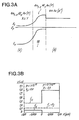
- the width of the potential barrier can be adjusted, as shown in FIGS. 3A and 3B, by moving the electrical junction relative to the GaAlAs - GaAs metallurgical junction, by placing a thin interface material 18 between the emitter and base regions.
- the material 18 is a layer of GaAlAs p-type - suitably doped and its thickness is easily adjustable, thus allowing easy adjustment of the width of the peak region.
- the doping level of the p - type material is chosen so that the layer 18 is completely depleted in normal operation, that the electron injection current depends mainly on the concentration of the minority carriers of the GaAs base region and that , therefore, the injection efficiency is still high.
- the doping level of the transmitter can be higher, for example 1017 cm -3 .
- FIG. 4A shows a heterojunction of the GaAlAs (N) - GaAs type (p + j similar to that illustrated in FIG. 1. But in this case, the expected peak 20, having a value ⁇ E c ' is set to ⁇ E' c by modifying the aluminum content in the interface region 22.
- This variation in aluminum concentration causes a variation in the field and makes it possible to modify the shape and the height of the crest, FIG. 4A shows a lower crest having linear slopes, but curves of more complex shape can be retained.
- the height of the effective barrier can be close to 0.3 eV even if X Al ⁇ 0.3.
- a band of energy for another hetero GaAlAs (N) - GaAs (p + ) junction is shown in Figure 4B.
- the aluminum content of the emitter layer is increased in the depletion layer and reduced at the interface, thereby changing the potential curve 24 provided to a new curve 26 and producing the desired value of the barrier voltage.
- the aluminum content of the N type GaAlAs emitter region can be greater than 30%, generally up to 45%.
- a slight progressive interface can be obtained (see FIG. 5) between the emitter layer and a thin layer 28 of p-type GaAlAs between the emitter and the base, this layer serving to displace the electrical junction relative to the metallurgical junction , as already described.
- This interface can lead to an X A1 > 0.30 between the layers N and p.
- the aluminum content can be reduced over a short distance in order to obtain a high field.
- FIG. 6 illustrates a structure 30 of quasi-planar transistor of the type illustrated in French patent 78 26 069. This structure can be obtained either by implantation or by diffusion, to put the basic contact on the same plane as that of the transmitter, by a p + type region, and this in the known manner, the doping and the width of the interfaces being adjusted for obtain the characteristics described above.
- a mesa structure of the type illustrated in Figure 7 (A to D) can be used, and is particularly suitable for progressive interfaces of the type described in connection with Figure 4B where X AlAs ⁇ 40 %.
- the manufacture of a mesa transistor such as transistor 32 is known in the prior art.
- FIG 8A Another structure using an emitter layer at the bottom is illustrated in Figure 8A.
- the transmitter inductance can be reduced to low values, which are suitable for high frequency operation.
- This structure can use a p-type implanted region as a base contact (CB) on the same plane as the collector contact (CC).
- CB base contact
- CC collector contact
- a second implantation isolation using protons, oxygen or boron for GaAs
- dotted area can be used to reduce the lateral emitter capacity (dotted area).
- the same transistor structure with emitter at the bottom can also be produced by mesa as shown in Figure 8.
- the base region can be obtained by etching and a self-aligned structure can be used to bring the base very closely into contact and the collector.
- An isolation layout of the emitter layer (area dotted line) below the base contact can reduce the stray capacitance between the transmitter and the base.
- the heterojunction semiconductor component according to the invention formed from group III-V compounds can be produced by epitaxial growth methods.
- this includes the GaAlAs - GaAs compounds; InP - GaInAs; AlGaAsIn - GaInAs; and AlInAs - GaInAs, pairs of other materials that can be considered at liquid nitrogen temperatures, such as GaSb - AlSb or InSb - CdTe.
Landscapes
- Bipolar Transistors (AREA)
Applications Claiming Priority (2)
| Application Number | Priority Date | Filing Date | Title |
|---|---|---|---|
| US41929382A | 1982-09-17 | 1982-09-17 | |
| US419293 | 1982-09-17 |
Publications (3)
| Publication Number | Publication Date |
|---|---|
| EP0106724A2 true EP0106724A2 (de) | 1984-04-25 |
| EP0106724A3 EP0106724A3 (en) | 1986-02-12 |
| EP0106724B1 EP0106724B1 (de) | 1989-06-07 |
Family
ID=23661636
Family Applications (1)
| Application Number | Title | Priority Date | Filing Date |
|---|---|---|---|
| EP83401740A Expired EP0106724B1 (de) | 1982-09-17 | 1983-09-02 | Balistischer bipolarer Transistor mit Heteroübergängen |
Country Status (5)
| Country | Link |
|---|---|
| EP (1) | EP0106724B1 (de) |
| JP (1) | JPS59210669A (de) |
| AU (1) | AU562454B2 (de) |
| CA (1) | CA1213378A (de) |
| DE (1) | DE3380047D1 (de) |
Cited By (7)
| Publication number | Priority date | Publication date | Assignee | Title |
|---|---|---|---|---|
| EP0273363A3 (en) * | 1986-12-22 | 1988-11-02 | Nec Corporation | Heterojunction bipolar transistor with ballistic operation |
| US4821082A (en) * | 1987-10-30 | 1989-04-11 | International Business Machines Corporation | Heterojunction bipolar transistor with substantially aligned energy levels |
| EP0197052B1 (de) * | 1984-09-21 | 1989-08-30 | AT&T Corp. | Eine neue halbleiteranordnung |
| US4866488A (en) * | 1985-03-29 | 1989-09-12 | Texas Instruments Incorporated | Ballistic transport filter and device |
| EP0257460A3 (en) * | 1986-08-12 | 1989-12-06 | Canon Kabushiki Kaisha | Solid-state electron beam generator |
| EP0619613A3 (de) * | 1993-04-07 | 1995-03-29 | Sharp Kk | Heteroübergang-Bipolartransistor. |
| FR2819342A1 (fr) * | 1988-11-02 | 2002-07-12 | Hughes Aircraft Co | Transistor bipolaire a heterojonction, a auto-alignement, et son procede de realisation |
Families Citing this family (24)
| Publication number | Priority date | Publication date | Assignee | Title |
|---|---|---|---|---|
| JPS59211267A (ja) * | 1983-05-17 | 1984-11-30 | Toshiba Corp | ヘテロ接合バイポ−ラトランジスタ |
| JPS6216569A (ja) * | 1985-07-16 | 1987-01-24 | Matsushita Electric Ind Co Ltd | ヘテロ接合トランジスタおよびその製造方法 |
| JPS6218762A (ja) * | 1985-07-18 | 1987-01-27 | Matsushita Electric Ind Co Ltd | ヘテロ接合トランジスタおよびその製造方法 |
| JPS6221272A (ja) * | 1985-07-19 | 1987-01-29 | Matsushita Electric Ind Co Ltd | ヘテロ接合トランジスタの製造方法 |
| JPS6247158A (ja) * | 1985-08-26 | 1987-02-28 | Matsushita Electric Ind Co Ltd | ヘテロ接合バイポ−ラトランジスタおよびその製造方法 |
| JPS6249656A (ja) * | 1985-08-29 | 1987-03-04 | Matsushita Electric Ind Co Ltd | ヘテロ接合バイポ−ラトランジスタおよびその製造方法 |
| JPS6249662A (ja) * | 1985-08-29 | 1987-03-04 | Matsushita Electric Ind Co Ltd | ヘテロ接合バイポ−ラトランジスタおよびその製造方法 |
| JPS6249657A (ja) * | 1985-08-29 | 1987-03-04 | Matsushita Electric Ind Co Ltd | ヘテロ接合バイポ−ラトランジスタおよびその製造方法 |
| JPS6249661A (ja) * | 1985-08-29 | 1987-03-04 | Matsushita Electric Ind Co Ltd | ヘテロ接合バイポ−ラトランジスタおよびその製造方法 |
| JPS6249658A (ja) * | 1985-08-29 | 1987-03-04 | Matsushita Electric Ind Co Ltd | ヘテロ接合バイポ−ラトランジスタおよびその製造方法 |
| JPS6249660A (ja) * | 1985-08-29 | 1987-03-04 | Matsushita Electric Ind Co Ltd | ヘテロ接合バイポ−ラトランジスタおよびその製造方法 |
| JPS6249659A (ja) * | 1985-08-29 | 1987-03-04 | Matsushita Electric Ind Co Ltd | ヘテロ接合バイポ−ラトランジスタおよびその製造方法 |
| JPH0611056B2 (ja) * | 1985-12-03 | 1994-02-09 | 富士通株式会社 | 高速半導体装置 |
| JPS6348863A (ja) * | 1986-08-19 | 1988-03-01 | Matsushita Electric Ind Co Ltd | ヘテロ接合バイポ−ラトランジスタの製造方法 |
| JPS6348862A (ja) * | 1986-08-19 | 1988-03-01 | Matsushita Electric Ind Co Ltd | ヘテロ接合バイポ−ラトランジスタの製造方法 |
| JPS63188969A (ja) * | 1987-01-30 | 1988-08-04 | Matsushita Electric Ind Co Ltd | バイポ−ラトランジスタの製造方法 |
| JPH0654780B2 (ja) * | 1987-02-19 | 1994-07-20 | 松下電器産業株式会社 | ヘテロ接合バイポーラトランジスタ |
| JPS63263761A (ja) * | 1987-04-22 | 1988-10-31 | Matsushita Electric Ind Co Ltd | バイポ−ラトランジスタの製造方法 |
| JPH0682678B2 (ja) * | 1987-05-07 | 1994-10-19 | 松下電器産業株式会社 | バイポーラトランジスタの製造方法 |
| JP2624253B2 (ja) * | 1987-05-07 | 1997-06-25 | 松下電器産業株式会社 | バイポーラトランジスタの製造方法 |
| JPH0824125B2 (ja) * | 1987-07-24 | 1996-03-06 | 松下電器産業株式会社 | バイポ−ラトランジスタおよびその製造方法 |
| JPH0824126B2 (ja) * | 1987-07-24 | 1996-03-06 | 松下電器産業株式会社 | バイポ−ラトランジスタおよびその製造方法 |
| JPH0824124B2 (ja) * | 1987-07-24 | 1996-03-06 | 松下電器産業株式会社 | バイポ−ラトランジスタの製造方法 |
| JPH0824127B2 (ja) * | 1987-07-24 | 1996-03-06 | 松下電器産業株式会社 | バイポ−ラトランジスタの製造方法 |
Family Cites Families (2)
| Publication number | Priority date | Publication date | Assignee | Title |
|---|---|---|---|---|
| JPS6024592B2 (ja) * | 1975-01-27 | 1985-06-13 | 株式会社日立製作所 | ワイドギヤツプエミツタトランジスタの製造方法 |
| US4366493A (en) * | 1980-06-20 | 1982-12-28 | International Business Machines Corporation | Semiconductor ballistic transport device |
-
1983
- 1983-09-02 DE DE8383401740T patent/DE3380047D1/de not_active Expired
- 1983-09-02 EP EP83401740A patent/EP0106724B1/de not_active Expired
- 1983-09-07 AU AU18791/83A patent/AU562454B2/en not_active Ceased
- 1983-09-13 CA CA000436549A patent/CA1213378A/en not_active Expired
- 1983-09-17 JP JP58172047A patent/JPS59210669A/ja active Granted
Cited By (8)
| Publication number | Priority date | Publication date | Assignee | Title |
|---|---|---|---|---|
| EP0197052B1 (de) * | 1984-09-21 | 1989-08-30 | AT&T Corp. | Eine neue halbleiteranordnung |
| US4866488A (en) * | 1985-03-29 | 1989-09-12 | Texas Instruments Incorporated | Ballistic transport filter and device |
| EP0257460A3 (en) * | 1986-08-12 | 1989-12-06 | Canon Kabushiki Kaisha | Solid-state electron beam generator |
| EP0273363A3 (en) * | 1986-12-22 | 1988-11-02 | Nec Corporation | Heterojunction bipolar transistor with ballistic operation |
| US4821082A (en) * | 1987-10-30 | 1989-04-11 | International Business Machines Corporation | Heterojunction bipolar transistor with substantially aligned energy levels |
| FR2819342A1 (fr) * | 1988-11-02 | 2002-07-12 | Hughes Aircraft Co | Transistor bipolaire a heterojonction, a auto-alignement, et son procede de realisation |
| EP0619613A3 (de) * | 1993-04-07 | 1995-03-29 | Sharp Kk | Heteroübergang-Bipolartransistor. |
| US5508536A (en) * | 1993-04-07 | 1996-04-16 | Sharp Kabushiki Kaisha | Heterojunction bipolar transistor having low electron and hole concentrations in the emitter-base junction region |
Also Published As
| Publication number | Publication date |
|---|---|
| CA1213378A (en) | 1986-10-28 |
| AU562454B2 (en) | 1987-06-11 |
| EP0106724A3 (en) | 1986-02-12 |
| AU1879183A (en) | 1984-03-22 |
| DE3380047D1 (en) | 1989-07-13 |
| JPH0586658B2 (de) | 1993-12-13 |
| EP0106724B1 (de) | 1989-06-07 |
| JPS59210669A (ja) | 1984-11-29 |
Similar Documents
| Publication | Publication Date | Title |
|---|---|---|
| EP0106724B1 (de) | Balistischer bipolarer Transistor mit Heteroübergängen | |
| EP3384537B1 (de) | Optoelektronische vorrichtung mit tridimensionalen halbleiterstrukturen in axialer konfiguration | |
| CN102144298B (zh) | 纳米结构的光电二极管 | |
| EP0236189B1 (de) | Monolithische Halbleiterstruktur eines Bipoltransistors mit Heteroübergängen und eines Lasers | |
| US9159873B2 (en) | High speed optical tilted charge devices and methods | |
| CN1259237A (zh) | 光电子半导体元件 | |
| FR2520157A1 (fr) | Dispositif semi-conducteur du genre transistor a heterojonction(s) | |
| EP2697831A1 (de) | Hemt-transistoren aus (iii-b) -n-halbleitern mit grossem bandabstand und mit bor | |
| US8148800B2 (en) | Nanowire-based semiconductor device and method employing removal of residual carriers | |
| FR3043251A1 (fr) | Transistor a effet de champ a rendement et gain optimise | |
| FR2743945A1 (fr) | Laser a semi-conducteur et procede de fabrication d'un tel laser | |
| EP0577498B1 (de) | Vertikaler JFET-Transistor mit optimiertem Betrieb und Verfahren zur Herstellung | |
| EP1764887B1 (de) | Optoelektronische Vorrichtung mit einem Laser mit integriertem Modulator und Herstellungsverfahren dafür | |
| EP0232662B1 (de) | Monolithische Halbleiterstruktur bestehend aus einem Laser und einem Feldeffekttransistor und deren Herstellungsverfahren | |
| FR2692721A1 (fr) | Procédé de réalisation de transistor bipolaire à hétérojonction et transistor obtenu. | |
| FR2819342A1 (fr) | Transistor bipolaire a heterojonction, a auto-alignement, et son procede de realisation | |
| CN115313155B (zh) | 一种异质隧道结的多结垂直腔面发射激光器及其制备方法 | |
| CN115173228B (zh) | 一种垂直腔面发射激光器及其制备方法 | |
| EP0684653B1 (de) | Lichtgesteuerter Heterostruktur-Halbleiterbaustein zur Erzeugung von Mikrowellen | |
| JPH0828327B2 (ja) | 半導体デバイスの製造方法 | |
| Capasso | New High-Speed Quantum Well and Variable Grap Superlattice Devices | |
| FR2519473A1 (fr) | Dispositif unipolaire a transfert d'electrons du type diode gunn | |
| Morozov et al. | Photoand electroluminescence in mid-infrared range from HgCdTe based waveguide structures | |
| FR3071854A1 (fr) | Procede de fabrication d'un composant electronique a heterojonction muni d'une couche barriere enterree | |
| TW201332238A (zh) | 光學傾斜電荷裝置及方法 |
Legal Events
| Date | Code | Title | Description |
|---|---|---|---|
| PUAI | Public reference made under article 153(3) epc to a published international application that has entered the european phase |
Free format text: ORIGINAL CODE: 0009012 |
|
| AK | Designated contracting states |
Designated state(s): DE FR GB IT NL |
|
| PUAL | Search report despatched |
Free format text: ORIGINAL CODE: 0009013 |
|
| AK | Designated contracting states |
Designated state(s): DE FR GB IT NL |
|
| 17P | Request for examination filed |
Effective date: 19860711 |
|
| 17Q | First examination report despatched |
Effective date: 19871020 |
|
| RAP1 | Party data changed (applicant data changed or rights of an application transferred) |
Owner name: ETAT FRANCAIS REPRESENTE PAR LE MINISTRE DES PTT ( |
|
| GRAA | (expected) grant |
Free format text: ORIGINAL CODE: 0009210 |
|
| AK | Designated contracting states |
Kind code of ref document: B1 Designated state(s): DE FR GB IT NL |
|
| REF | Corresponds to: |
Ref document number: 3380047 Country of ref document: DE Date of ref document: 19890713 |
|
| ITF | It: translation for a ep patent filed | ||
| ITTA | It: last paid annual fee | ||
| PGFP | Annual fee paid to national office [announced via postgrant information from national office to epo] |
Ref country code: NL Payment date: 19890930 Year of fee payment: 7 |
|
| GBT | Gb: translation of ep patent filed (gb section 77(6)(a)/1977) | ||
| PLBE | No opposition filed within time limit |
Free format text: ORIGINAL CODE: 0009261 |
|
| STAA | Information on the status of an ep patent application or granted ep patent |
Free format text: STATUS: NO OPPOSITION FILED WITHIN TIME LIMIT |
|
| 26N | No opposition filed | ||
| PG25 | Lapsed in a contracting state [announced via postgrant information from national office to epo] |
Ref country code: NL Effective date: 19910401 |
|
| NLV4 | Nl: lapsed or anulled due to non-payment of the annual fee | ||
| PGFP | Annual fee paid to national office [announced via postgrant information from national office to epo] |
Ref country code: GB Payment date: 19940830 Year of fee payment: 12 |
|
| PGFP | Annual fee paid to national office [announced via postgrant information from national office to epo] |
Ref country code: DE Payment date: 19940912 Year of fee payment: 12 |
|
| PGFP | Annual fee paid to national office [announced via postgrant information from national office to epo] |
Ref country code: FR Payment date: 19940923 Year of fee payment: 12 |
|
| PG25 | Lapsed in a contracting state [announced via postgrant information from national office to epo] |
Ref country code: GB Effective date: 19950902 |
|
| GBPC | Gb: european patent ceased through non-payment of renewal fee |
Effective date: 19950902 |
|
| PG25 | Lapsed in a contracting state [announced via postgrant information from national office to epo] |
Ref country code: FR Effective date: 19960531 |
|
| PG25 | Lapsed in a contracting state [announced via postgrant information from national office to epo] |
Ref country code: DE Effective date: 19960601 |
|
| REG | Reference to a national code |
Ref country code: FR Ref legal event code: ST |