EP0107416A2 - Verfahren zur Herstellung einer Halbleiteranordnung - Google Patents
Verfahren zur Herstellung einer Halbleiteranordnung Download PDFInfo
- Publication number
- EP0107416A2 EP0107416A2 EP83305971A EP83305971A EP0107416A2 EP 0107416 A2 EP0107416 A2 EP 0107416A2 EP 83305971 A EP83305971 A EP 83305971A EP 83305971 A EP83305971 A EP 83305971A EP 0107416 A2 EP0107416 A2 EP 0107416A2
- Authority
- EP
- European Patent Office
- Prior art keywords
- film
- conductive film
- semiconductor substrate
- forming
- polycrystalline silicon
- Prior art date
- Legal status (The legal status is an assumption and is not a legal conclusion. Google has not performed a legal analysis and makes no representation as to the accuracy of the status listed.)
- Granted
Links
Images





Classifications
-
- H—ELECTRICITY
- H10—SEMICONDUCTOR DEVICES; ELECTRIC SOLID-STATE DEVICES NOT OTHERWISE PROVIDED FOR
- H10W—GENERIC PACKAGES, INTERCONNECTIONS, CONNECTORS OR OTHER CONSTRUCTIONAL DETAILS OF DEVICES COVERED BY CLASS H10
- H10W20/00—Interconnections in chips, wafers or substrates
- H10W20/01—Manufacture or treatment
- H10W20/031—Manufacture or treatment of conductive parts of the interconnections
- H10W20/056—Manufacture or treatment of conductive parts of the interconnections by filling conductive material into holes, grooves or trenches
- H10W20/058—Manufacture or treatment of conductive parts of the interconnections by filling conductive material into holes, grooves or trenches by depositing on sacrificial masks, e.g. using lift-off
-
- H—ELECTRICITY
- H10—SEMICONDUCTOR DEVICES; ELECTRIC SOLID-STATE DEVICES NOT OTHERWISE PROVIDED FOR
- H10P—GENERIC PROCESSES OR APPARATUS FOR THE MANUFACTURE OR TREATMENT OF DEVICES COVERED BY CLASS H10
- H10P50/00—Etching of wafers, substrates or parts of devices
- H10P50/20—Dry etching; Plasma etching; Reactive-ion etching
- H10P50/26—Dry etching; Plasma etching; Reactive-ion etching of conductive or resistive materials
- H10P50/264—Dry etching; Plasma etching; Reactive-ion etching of conductive or resistive materials by chemical means
- H10P50/266—Dry etching; Plasma etching; Reactive-ion etching of conductive or resistive materials by chemical means by vapour etching only
- H10P50/267—Dry etching; Plasma etching; Reactive-ion etching of conductive or resistive materials by chemical means by vapour etching only using plasmas
- H10P50/268—Dry etching; Plasma etching; Reactive-ion etching of conductive or resistive materials by chemical means by vapour etching only using plasmas of silicon-containing layers
-
- H—ELECTRICITY
- H10—SEMICONDUCTOR DEVICES; ELECTRIC SOLID-STATE DEVICES NOT OTHERWISE PROVIDED FOR
- H10P—GENERIC PROCESSES OR APPARATUS FOR THE MANUFACTURE OR TREATMENT OF DEVICES COVERED BY CLASS H10
- H10P50/00—Etching of wafers, substrates or parts of devices
- H10P50/20—Dry etching; Plasma etching; Reactive-ion etching
- H10P50/28—Dry etching; Plasma etching; Reactive-ion etching of insulating materials
- H10P50/282—Dry etching; Plasma etching; Reactive-ion etching of insulating materials of inorganic materials
- H10P50/283—Dry etching; Plasma etching; Reactive-ion etching of insulating materials of inorganic materials by chemical means
-
- H—ELECTRICITY
- H10—SEMICONDUCTOR DEVICES; ELECTRIC SOLID-STATE DEVICES NOT OTHERWISE PROVIDED FOR
- H10P—GENERIC PROCESSES OR APPARATUS FOR THE MANUFACTURE OR TREATMENT OF DEVICES COVERED BY CLASS H10
- H10P76/00—Manufacture or treatment of masks on semiconductor bodies, e.g. by lithography or photolithography
- H10P76/40—Manufacture or treatment of masks on semiconductor bodies, e.g. by lithography or photolithography of masks comprising inorganic materials
-
- Y—GENERAL TAGGING OF NEW TECHNOLOGICAL DEVELOPMENTS; GENERAL TAGGING OF CROSS-SECTIONAL TECHNOLOGIES SPANNING OVER SEVERAL SECTIONS OF THE IPC; TECHNICAL SUBJECTS COVERED BY FORMER USPC CROSS-REFERENCE ART COLLECTIONS [XRACs] AND DIGESTS
- Y10—TECHNICAL SUBJECTS COVERED BY FORMER USPC
- Y10S—TECHNICAL SUBJECTS COVERED BY FORMER USPC CROSS-REFERENCE ART COLLECTIONS [XRACs] AND DIGESTS
- Y10S438/00—Semiconductor device manufacturing: process
- Y10S438/965—Shaped junction formation
Definitions
- the present invention relates to a method of producing a semiconductor device, such as an integrated circuit (IC) of bipolar transistors or metal oxide semiconductor (MOS) transistors.
- IC integrated circuit
- MOS metal oxide semiconductor
- An object of the present invention is to produce a denser semiconductor device by utilizing an improved self-alignment system.
- Another object of the present invention is to decrease the area required for electrodes coming into contact with a base contact region, a source region, and a drain region, and to decrease the area of a base region including the base contact region, the source region, and the drain region, so as to decrease the parasitic capacitance to increase the operating speed and so as to increase the degree of integration.
- Still another object of the present invention is to provide a method of producing by self-alignment an MOS semiconductor device without use of a polycrystalline silicon gate as a mask.
- a method of producing a semiconductor device which comprises the steps of: (a) forming a first insulating film on a semiconductor substrate; (b) forming a first conductive film on the first insulating film; (c) forming a first masking film having a window on the conductive film; (d) selectively etching the first conductive film to form an opening having similar dimensions to those of the window; (e) transversely etching the first conductive film to enlarge the opening and to form a protruding portion of the first masking film; (f) forming a second masking film on the first insulating film through the window; (g) selectively etching an uncovered portion of the first insulating film under the protruding portion to expose a surface portion of the semiconductor substrate; and (h) forming a second conductive film connecting the first conductive film and the exposed surface portion of the semiconductor substrate.
- only one mask is used for forming a window of the masking film after which steps (d) through (h) can be carried out by self-alignment.
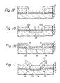
- FIG. 1A A process for producing a bipolar semiconductor device in accordance with a first embodiment of the present invention, is illustrated in Figs. 1A to lI.
- a thin silicon dioxide (Si0 2 ) film 2 having a thickness of, e.g., approximately 50 nm is formed on a semiconductor substrate 1 by thermal oxidizing the silicon substrate 1.
- the substrate 1 comprises an N-type silicon semiconductor layer and a P-type silicon semiconductor substrate having an N +- type buried layer, the N-type layer being epitaxially grown on the P-type substrate.
- a silicon nitride (Si 3 N 4 ) film 3 having a thickness of, e.g., approximately 100 nm is formed on the Si0 2 film 2 by a chemical vapor deposition (CVD) method.
- the Si0 2 film 2 and Si 3 N 4 film 3 serve as an insulating film.
- a first polycrystalline silicon film (a first conductive film) 4 which is doped with boron of, e.g., approximately 1 x 10 20 /cm 3 and has a thickness of, e.g., approximately 300 nm is formed on the Si 3 N 4 film 3 by a low pressure CVD (LPCVD) method.
- LPCVD low pressure CVD
- a SiO 2 film 5 having a thickness of, e.g., approximately 200 nm is formed on the first polycrystalline silicon film 4 by a CVD method.
- a resist film e.g., a photoresist film 6 is spin coated on the Si0 2 film 5, exposed, and developed to form a window 7.
- the exposure is performed with a patterned light through a mask (i.e., a photomask).
- An electron beam exposure may be used by using electron beam resist instead of the photoresist 6.
- the SiO 2 film 5 and the polycrystalline silicon film 4 are successively anisotropically etched by using the resist film 6 (i.e., a first masking film) as a mask, so that an opening 8 having similar dimensions to the window 7 is formed.
- the etching steps are carried out by utilizing a reactive ion etching method using CHF 3 gas or CC1 4 gas as an etchant.
- the SiO 2 film 5 is transversely etched so as to enlarge the opening 8 by means of a buffer solution of hydrofluoric acid, e.g., a solution of HF/NH 4 F. Then, the first polycrystalline silicon film 4 is also transversely etched by a plasma etching method using a mixture of CF 4 gas and 0 2 gas. Thus, an protruding portion of the resist film 6 is formed around the window 7 and a cavity 9 having a depth of, e.g., approximately 200 nm is formed under the protruding portion.
- a buffer solution of hydrofluoric acid e.g., a solution of HF/NH 4 F.
- the first polycrystalline silicon film 4 is also transversely etched by a plasma etching method using a mixture of CF 4 gas and 0 2 gas.
- a cavity 9 having a depth of, e.g., approximately 200 nm is formed under the protruding portion.
- Al aluminum
- a vacuum deposition method or a sputtering method to form an Al film 10a and another Al film (a second masking film) lOb, respectively.
- the Al film 10b covers a portion of the Si 3 N 4 film 3 but does not cover the portion of the film 3 under the protruding of the resist film 6, as shown in Fig. 1C.
- the resist film 6 is removed by means of a solvent, whereupon the Al.film 10a on the resist film 6 is also removed.
- Such removal of the Al film is called a lift-off process.
- only the Al film 10b remains.
- the Si 3 N 4 film 3 and the Si0 2 film 2 are selectively etched by a reactive ion etching method using a gas etchant, e.g., CHF 3 gas or a mixture of CF 4 and 0 2 gas (CF 4 /0 2 gas) to form an opening 11.
- a gas etchant e.g., CHF 3 gas or a mixture of CF 4 and 0 2 gas (CF 4 /0 2 gas)
- CF 4 /0 2 gas CF 4 /0 2 gas
- a second polycrystalline silicon film 12 having a thickness of, e.g., 400 nm is formed on the SiO 2 film 5, the Si 3 N 4 film 3 and the exposed portion of the semiconductor substrate 1 by a LPCVD method.
- the second polycrystalline silicon film 12 is anisotropically etched in a direction perpendicular to the semiconductor substrate 1 to expose at least the Si 3 N 4 film 3 by a reactive ion etching method using CC1 4 gas or CF 4 /0 2 gas as an etchant.
- a portion 12a of polycrystalline silicon remains so as to adjoin the wall of the opening 8, i.e., the sides of the Si0 2 film 5 and the first polycrystalline silicon film 4.
- the polycrystalline silicon portion 12a serves as a second conductive film connecting the first polycrystalline silicon film 4 and the semiconductor substrate 1.
- P-type impurities e.g., boron ions are introduced into the semiconductor substrate 1 through the Si 3 N 4 film 3 and the Si0 2 film 2 by an ion-implantation method to form a base (P-type) region 14.
- boron ion dose of approximately 8 x 10 12 ions/cm2 is used.
- the obtained semiconductor device is heat-treated under a wet oxidizing atmosphere at a temperature of 900°C to oxidize the polycrystalline silicon portion 12a, so that a Si0 2 film 15 having a thickness of approximately 200 nm is formed.
- boron contained in the first polycrystalline silicon 4 diffuses into the semiconductor substrate 1 through the polycrystalline silicon portion 12a to form a P +- type region (i.e., a base contact region) 16.
- the Si 3 N 4 film 3 and the SiO 2 film 2 are anisotropically etched by a reactive ion etching method to expose a surface of the semiconductor substrate 1 in the base region 14.
- the SiO 2 film 15 is also etched to decrease the thickness thereof.
- the SiO 2 film 15 remains.
- the above-mentioned steps of the formation of the opening 8 through the step of the removal of the Si 3 N 4 film 3 and the SiO 3 film 2 can be carried out by self-alignmently carried out without using any masks.
- a third polycrystalline silicon film doped with N-type impurities, e.g., arsenic is formed on the SiO 2 film 5 and the base region 14 of the semiconductor substrate 1 by a LPCVD method and is patterned by a conventional lithographic method (e.g., a photo-lithographic method) to form an emitter electrode 19 of the third polycrystalline silicon film. It is possible to use a doped silicide instead of polycrystalline silicon. Then, heat-treatment (at approximately 1000°C for 10 minutes) is carried out so as to diffuse arsenic out of the emitter electrode 19 into the semiconductor substrate 1 within the base region 14, so that an N +- type region (an emitter region) 20 is formed.
- N-type impurities e.g., arsenic
- a bipolar transistor having an emitter region 20 of a length not more than 0.5 ⁇ m and of a base region 14 and base contact region 16 of a total length not more than 1.5 ⁇ m.
- the base contact region 16, the base region 14, and the emitter region 20 can be formed by self-alignment without taking any alignment margin into consideration. Accordingly, the the regions can be formed smaller, and a denser bipolar semiconductor device can be produced. As a result, parasitic capacitance can be decreased and performance of the bipolar transistor can be improved.
- FIG. 2A to 2H A process for producing a bipolar semiconductor device in accordance with a second embodiment of the present invention is illustrated in Figs. 2A to 2H.
- a semiconductor substrate 21, a Si0 2 film 22, a Si 3 N 4 film 23, and a first polycrystalline silicon film 24 doped with boron correspond to the semiconductor substrate 1, the Si0 2 film 2, the Si 3 N 4 film 3, and the first polycrystalline silicon film 4 in the first embodiment, respectively, and are formed in the same manner as described in the first embodiment.
- a Si0 2 film 25 having a thickness of, e.g., approximately 200 nm is formed on the first polycrystalline silicon film 24 by thermally oxidizing the polycrystalline silicon.
- a resist film (a photoresist film) 26 is spin coated on the SiO 2 film 25, exposed, and developed to form a window 27. The exposure is performed with patterned light through a photomask.
- the SiO 2 film 5 and the first polycrystalline silicon film 24 are successively anisotropically etched by using the resist film 26 as a mask, so that an opening 28 having similar dimensions to those of the window 27 is formed.
- P-type impurities e.g., boron ions are introduced into the semiconductor substrate 21 at a dose of approximately 8 x 10 12 ions/cm 2 by an ion-implantation method, so that a base (P-type) region 29 is formed.
- the resist film 26 is removed. The removal of the resist film 26 may be carried out before the ion-implantation step.
- the first polycrystalline silicon film 24 is transversely etched so as to enlarge the opening 28 by a plasma etching method using a CF 4 /0 2 gas.
- the Si0 2 film 25 serves as a first masking film.
- an protruding portion 25a of the SiO 2 film 25 appears and a cavity 30 having a depth of, e.g., approximately 200 nm is formed under the protruding portion.
- A1 is deposited on the SiO 2 film 25 and on the Si 3 N 4 film 23 through the opening 28 by a vacuum deposition method or a sputtering method to form an Al film 31a and another Al film (a second masking film) 31b, respectively.
- the A1 film 31b does not cover the portion of the Si 3 N 4 film 23 under the protruding portion 25a.
- the Al films 31a and 31b as masks, the uncovered portion of the Si 3 N 4 film 23 is etched by a plasma etching method using a CF 4 /0 2 gas as an etchant. Then, the Al film 31a and 3lb are removed.
- the portion of the SiO 2 film 22 under the protruding portion 25a is etched by a wet etching method using a solution of HF/NH 4 F to form an opening 32 wherein a portion of the semiconductor substrate 21 is exposed.
- the SiO 2 film 25 is also etched to decrease the thickness thereof. However, since the SiO 2 film 25 is relatively thick, it remains.
- the LPCVD features in good surface coverage whereby the cavity 30 and the opening 32 are filled with polycrystalline silicon.
- the second polycrystalline silicon film 33 is anisotropically etched to expose at least the Si 3 N 4 film 23 by a reactive ion etching method using CC1 4 gas or CF 4 /0 2 gas as an etchant. Therefore, a portion 33a of the second polycrystalline silicon film 33 remains under the protruding portion 25a.
- the first polycrystalline silicon film 24 and the polycrystalline silicon portion 33a are thermally oxidized to form a SiO 2 film 34 having a thickness of, e.g., approximately 200 nm.
- boron contained in the first polycrystalline silicon film 24 diffuses into the semiconductor substrate 21 through the polycrystalline silicon portion 33a to form a P +- type region (a base contact region) 35.
- the exposed portion of the Si 3 N 4 film 23 is etched and then the Si0 2 film 22 is etched to expose a surface of the semiconductor substrate 1 in the base region 29.
- the Si0 2 film 34 is also etched to decrease the thickness thereof.
- the Si0 2 film 34 is relatively thick, it remains.
- a third polycrystalline silicon film doped with arsenic is formed on the Si0 2 film 34 and the base region 29 of the semiconductor substrate 21 by a LPCVD method and is patterned by a photo-lithographic method to form an emitter electrode 36.
- Heat-treatment is carried out so as to diffuse arsenic out of the emitter electrode 36 of the third polycrystalline silicon film into the semiconductor substrate 21 within the base region 29, so that an N +- type region (an emitter region) 37 is formed.
- N +- type region an emitter region
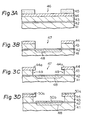
- FIG. 3A to 3H A process for producing a bipolar semiconductor device in accordance with a third embodiment of the present invention is illustrated in Figs. 3A to 3H.
- a semiconductor substrate 41 of (111) plane silicon is thermally oxidized to form a SiO 2 film 42 having a thickness of, e.g., approximately 80 nm.
- the substrate 1 comprises an N-type silicon layer and a P-type single crystalline silicon substrate having a N +- type buried layer, the N-type layer being epitaxially grown on the P-type substrate.
- a first polycrystalline silicon film 43 doped with boron and having a thickness of, e.g., approximately 300 nm is formed on the Si0 2 film 42 by a LPCVD method.
- a Si0 2 film 44 having a thickness of approximately 400 nm is formed on the first polycrystalline silicon film 43 by a CVD method.
- a photoresist film 45 is spin coated on the Si0 2 film 44, exposed, and developed to form a window 46. The exposure is performed with patterned light through a photomask.
- the SiO 2 film 44 and the polycrystalline silicon film 43 are anisotropically etched by a reactive ion etching method to form an opening 47 having similar dimensions to the window 46.
- the photoresist film 45 is removed by means of a solvent.
- boron ions are introduced into the semiconductor substrate 41 at a dose of approximately 8 x 10 12 ions/cm 2 by an ion--implantation method, so that a base (P-type) region 48 is formed.
- the polycrystalline silicon film 43 is transversely etched by a plasma etching method using a CF 4 /0 2 gas as an etchant. It is possible to utilize a wet etching method instead of the plasma etching method. Thus, an protruding portion 44a of the Si0 2 film 44 appears and a cavity 49 having a depth of, e.g., approximately 200 nm is formed under the protruding portion 44a.
- silicon nitride (Si 3 N 4 ) is deposited on the Si0 2 film 44 and on a portion of the SiO 2 film 42 through the opening 47 by a sputtering method to form a first Si 3 N 4 film 50a and a second Si 3 N 4 film (a second masking film) 50b, the Si 3 N 4 film having a thickness of, e.g., approximately 100 nm.
- the second Si 3 N 4 film 50b does not cover the portion of the Si0 2 film 42 under the overhang portion 44a.
- the Si0 2 film 42 is selectively etched through the cavity 49 by a wet etching method using a solution of HF and NH 4 F as an etchant, to form an opening 51.
- a portion of the semiconductor substrate 41 is exposed.
- a second polycrystalline silicon film 52 having a thickness of, e.g., 400 nm is formed on the Si 3 N 4 films 50a and 50b and within the cavity 49 and the opening 51 by a LPCVD method.
- the second polycrystalline silicon film 52 is anisotropically etched to expose the second Si 3 N 4 film 50b by a reactive ion etching method using CC1 4 gas or CF 4 /0 2 gas as an etchant. As a result of the etching, a portion 52a of the second polycrystalline silicon film 52 remains so as to fill the cavity 49.
- the polycrystalline silicon portion 52a is thermally oxidized to form a SiO 2 film 53 having a thickness of, e.g., approximately 200 nm.
- boron contained in the first polycrystalline silicon 43 diffuses into the semiconductor substrate 41 through the polycrystalline silicon portion 52a to form a P +- type region (a base contact region) 54.
- reactive ion etching is carried out so as to remove the exposed portion of the second Si 3 N 4 film 50b and the portion of the SiO 2 film 42 to expose a surface of the semiconductor substrate 41.
- the first Si 3 N 4 film 50a is inevitably etched out and the SiO 2 films 44 and 53 are also etched to decrease the thickness thereof. In this case, since the Si0 2 films 44 and 53 are relatively thick, they remain.
- a third polycrystalline silicon film doped with arsenic is formed on the remaining Si0 2 films 44 and 53 and the exposed surface of the semiconductor substrate 41 by a LPCVD method and is patterned (i.e., selectively etched) by a photo-lithographic method to form an emitter electrode 55.
- Heat-treatment is carried out so as to diffuse arsenic out of the emitter electrode 55 of the third polycrystalline silicon film into the semiconductor substrate 41 in the base region 48, so that an emitter region (an N +- type region 56 is formed.
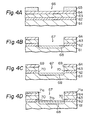
- FIG. 4A to 4G A process for producing a bipolar semiconductor device in accordance with a fourth embodiment of the present invention is illustrated in Figs. 4A to 4G.
- a SiO 2 film 62 having a thickness of, e.g., 300 nm is formed on a semiconductor substrate 61 of (111) plane silicon by a CVD method.
- the substrate 61 comprises an N-type silicon expitaxial layer and a P-type silicon single crystalline substrate with a N +- type buried layer.
- a first polycrystalline silicon film 63 doped with boron and having a thickness of, e.g., approximately 300 nm is formed on the Si0 2 film 62 by a LPCVD method.
- a Si 3 N 4 insulating film 64 having a thickness of, e.g., approximately 300 nm is formed on the polycrystalline silicon film 63 by a sputtering method.
- a photoresist film 65 is spin coated on the Si 3 N 4 insulating film 64, exposed, and developed to form a window 66. The exposure is performed with patterned light through a photomask.
- the SiO insulating film 64 and the polycrystalline silicon film 63 are successively anisotropically etched by a reactive ion etching method to form an opening 67.
- the dimensions of the opening 67 are similar to those of the window 66.
- boron ions are directly introduced into the semiconductor substrate 61 at a dose of approximately 8 x 10 12 ions/cm 2 by an ion-implantation method, to form a base (P-type) region 68.
- the Si0 2 film 62 is transversely etched by a wet etching method using a mixture solution of HF and NH 4 F as an etchant. Therefore, an protruding portion 69 consisting of portions of the Si 3 N 4 insulating film 64 and the polycrystalline silicon film 63 is formed, and a cavity 70 having a depth of, e.g., 200 nm is formed under the protruding portion 69.
- Si 3 N 4 is deposited on the Si 3 N 4 insulating film 64 and on a portion of the semiconductor substrate 61 through the opening 67 by a sputtering method, so that a first Si 3 N 4 film 71a and a second Si 3 N 4* film 71b having a thickness of, e.g., approximately 100 nm are formed.
- the second Si 3 N 4 film 71b does not cover the portion of the semiconductor substrate 61 under the protruding portion 69.
- a second polycrystalline silicon film 72 having a thickness of, e.g., 400 nm is formed on the Si 3 N 4 films 71a and 71b and within the cavity 70 by a LPCVD method.
- the second polycrystalline silicon film 72 is anisotropically etched to expose the second Si 3 N 4 film 71b by a reactive ion etching. As a result of the etching, a portion 72a of the second polycrystalline silicon film 72 remains so as to fill the cavity 70.
- the polycrystalline silicon portion 72a is thermally oxidized to form a Si0 2 film 73 having a thickness of, e.g., approximately 200 nm.
- boron contained in the first polycrystalline silicon 63 diffuses into the semiconductor substrate 61 through the polycrystalline silicon portion 72a to form a P + -type region (a base contact region) 76.
- the exposed portion of the Si 3 N 4 film 71b is etched by a reactive ion etching method or a wet etching method using a solution of hot phosphoric acid to expose a surface of the semiconductor substrate 61.
- the first Si 3 N 4 film 71a is also etched out.
- a third polycrystalline silicon film doped with arsenic is formed by a LPCVD method and is patterned by a photo-lithographic method to form an emitter electrode 75. Heat-treatment is carried out so as to diffuse arsenic out of the emitter electrode 75 into the semiconductor substrate 61, so that an emitter (N +- type) region 76 is formed in the base region 68.
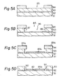
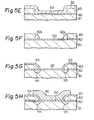
- FIG. 5A to 5H A process for producing an MOS semiconductor device in accordance with a fifth embodiment of the present invention is illustrated in Figs. 5A to 5H.
- a Si 3 N 4 film 82 having a thickness of, e.g., approximately 100 nm is formed on a P-type silicon semiconductor substrate 81 with a thick filed oxide film (not shown) by a CVD method. It is possible to form a double layer film composed of a Si0 2 film and a Si 3 N 4 film instead of the Si 3 N 4 film 82.
- the double layer may consist of a Si0 2 film which is formed by a thermal oxidation method and has a thickness of, e.g., 50 nm and a Si 3 N 4 film which is formed on the Si0 2 film by a CVD method and has a thickness of, e.g., 100 nm.
- a first polycrystalline silicon film 83 doped with arsenic and having a thickness of, e.g., 400 nm is formed on the Si 3 N 4 film 82 by a LPCVD method.
- a photoresist film 84 is spin coated on the polycrystalline silicon film 83, exposed, and developed to form a window 85 and to expose the surface of the polycrystalline silicon film over unactive area of the element and over the field oxide layer. The exposure is performed with light through a photomask having a predetermined pattern.
- the first polycrystalline silicon film 83 is anisotropically etched by a reactive ion etching method to form an opening 86, the dimensions of which are similar to the window 85. Subsequently, the polycrystalline silicon film 83 is transversely etched so as to enlarge the opening 86 by a wet etching method or a plasma etching method using a mixture gas of CF 4 gas and 0 2 gas as an etchant. As a result of these etching treatments, protruding portions of the photoresist film 84 appear and the cavities 87 and 88 having a depth of, e.g., 200 nm are formed under the protruding portions.
- Al is deposited by a vacuum deposition method or a sputtering method to form a first Al film 89a on the photoresist film 84 and a second Al film (a second masking film) 89b on the Si 3 N 4 film 82, the thickness of the Al films being, e.g., 100 nm.
- the second A1 film 89b does not cover the portion of the Si 3 N 4 film 82 under the protruding portions.
- the photoresist film 84 is removed by means of a solvent, whereupon the first Al film 89a on the photoresist film 84 is removed.
- the Si 3 N 4 film 82 is selectively etched to form narrow stripe openings 90 and 91 by a reactive ion etching method using a CF 4 /0 2 gas as an etchant.
- the polycrystalline silicon film 83 is-Etched to decrease the thickness thereof, but still remains.
- a second polycrystalline silicon film 92 having a thickness of, e.g., 300 nm is formed on the first polycrystalline silicon film 83 and the Si 3 N 4 film 82 and within the openings 90 and 91 by a LPCVD method.
- the second polycrystalline silicon film 92 is anisotropically etched so as to expose the Si 3 N 4 film 82 by a reactive ion etching method using CC1 4 gas or CF 4 /0 2 gas as an etchant. As a result of the etching, portions 92a and 92b adjoining the walls of the cavities 87 and 88 can remain.
- the first polycrystalline silicon film 83 and the polycrystalline silicon portions 92a and 92b are thermally oxidized to form a Si0 2 film 93 having thickness of, e.g., 200 nm.
- arsenic contained in the first polycrystalline silicon film 83 diffuses into the semicondutor substrate 81 through the polycrystalline silicon portions 92a and 92b to form N +- type regions, i.e., a source region 94 and a drain region 95, respectively.
- an Al film is formed on the sio 2 film 93 and the Si 3 N 4 film 82 by a sputtering method or a vacuum deposition method and is patterned (i.e., selectively etched) by a photo-lithographic method to form a gate electrode 96.
- the Si 3 N 4 film 82 under the gate electrode 96 serves as a gate insulating film.
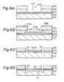
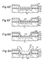
- FIG. 6A to 6H A process for producing a bipolar semiconductor device provided with a metal silicide film as a second conductive film in accordance with a sixth embodiment of the present invention is illustrated in Figs. 6A to 6H.
- a silicon semiconductor substrate 101 is thermally oxidized to form a Si0 2 film 102 having a thickness of, e.g., 50 nm.
- the substrate 101 comprises an N-type silicon layer and a P-type single crystalline silicon substrate having an N +- type buried layer, the N-type layer being epitaxially grown on the P-type substrate.
- a Si 3 N 4 film 103 having a thickness of, e.g., 100 nm is formed on the Si0 2 film 102 by a CVD method.
- a polycrystalline silicon film 104 which is doped with boron of, e.g., 1 x 10 20 /cm 3 and has a thickness of, e.g., 300 nm is formed on the Si 3 N 4 film 103 by a LPCVD method.
- a photoresist film 105 is spin coated on the polycrystalline silicon film 104, exposed, and developed to form a window 106. When the exposure is carried out, a photomask with a predetermined pattern is used. Then, the polycrystalline silicon film 104 is anisotropically etched through the window 106 by a reactive ion etching method to form an opening 107 having similar dimensions to those of the window 106.
- the polycrystalline silicon film 104 is further transversely etched so as to enlarge the opening 107 by a plasma etching method or a wet etching method. Accordingly, a protruding portion of the resist film 105 is formed around the window 106, and a cavity 108 is formed under the protruding portion.
- A1 is deposited by a vacuum deposition method or a sputtering method to form a first Al film 109a on the photoresist film 104 and a second Al film 109b on the Si 3 N 4 film 103, respectively.
- the second A1 film 109b does not cover the portion of the Si 3 N 4 film 103 under the protruding portion.
- the photoresist film 105 is removed, whereupon the first Al film 109a is also removed.
- the Si 3 N 4 film 103 and the Si0 2 film 102 are successively selectively etched by utilizing a suitable etching method to form an opening 110 in which a portion of the semiconductor substrate 101 is exposed.
- the second Al film 109b is removed by a wet etching method. Then, boron ions are introduced into the semiconductor substrate 101 by an ion-implantation method to form a base (P-type) region 111.
- a metal film 112 having a thickness of, e.g., 150 nm is formed on the polycrystalline silicon film 104 and the Si 3 N 4 film 103 and within the opening 110 by a sputtering method or a vacuum deposition method.
- the metal of film 112 should react with silicon to form metal silicide.
- the metal may be molybdenum, tungsten, titanium, tantalum, platinum, zirconium or hafnium
- the metal silicide may be molybdenum silicide (MoSi 2 ), tungsten silicide (WSi 2 ), titanium silicide (TiSi 2 ), tantalum silicide (TaSi 2 ), platinum silicide (PtSi 2 ), zirconium silicide (ZrSi 2 ), or hafnium silicide (HfSi 2 ).
- MoSi 2 molybdenum silicide
- WSi 2 tungsten silicide
- TiSi 2 titanium silicide
- TaSi 2 tantalum silicide
- ZrSi 2 zirconium silicide
- HfSi 2 hafnium silicide
- heat treatment e.g., at 600°C for 30 minutes under a nitrogen atmosphere
- heat treatment is performed so as to convert a portion of the Mo film 112 coming into contact with the polycrystalline silicon film 104 and the silicon semiconductor substrate 101 into a MoSi 2 film 113.
- the portion of the Mo film 112 on the Si 3 N 4 film 103 remains.
- the MoSi 2 film 13 is thermally oxidized to form a SiO 2 film 114.
- an insulating film of Si0 2 , Si 3 N 4 or phosphosilicate glass may be selectively formed on the MoSi 2 film 113 by a CVD method.
- the exposed portion of the Si 3 N 4 film 103 and the Si0 2 film 102 under it are etched by using a suitable etchant to expose a portion of the semiconductor substrate 101 in the base region 111.
- another polycrystalline silicon film doped with arsenic is formed on the exposed semiconductor substrate 101 and the insulating film 114 by a LPCVD method and is patterned by a photo-lithographic method to form an emitter electrode 115.
- Heat treatment is carried out so as to diffuse arsenic out of the emitter electrode 115 into the semiconductor substrate 101, so that an N +- type region (an emitter region) 116 is formed within the base region 111.
- the metal silicide film having a lower electric resistance than that of doped polycrystalline silicon is used as a part of the base electrode, an external base resistance can be reduced as compared with a base electrode comprised of doped polycrystalline silicon. Accordingly, it is possible to increase the operating speed and to decrease dissipation power of a bipolar transistor.
- a base region can be formed by an ion-implantation method.
- Another photoresist film (not shown) is selectively formed in the opening 107 on a portion of the Si 3 N 4 film 103 corresponding to an emitter electrode contact window, so as to expose another portion of the Si 3 N 4 film 103 corresponding to a base electrode contact window.
- the exposed portion of the Si 3 N 4 film 103 and the portion of the Si0 2 film 102 being under it are selectively etched by utilizing a suitable etching method to form the opening 110, as illustrated in Fig. 6C.
- a device similar to that illustrated in Fig. 6D is obtained.
- a base electrode and an emitter electrode can be formed in a similar manner to that described in the fixth embodiment, referring to Figs. 6E through 6H.
Landscapes
- Bipolar Transistors (AREA)
Applications Claiming Priority (8)
| Application Number | Priority Date | Filing Date | Title |
|---|---|---|---|
| JP172027/82 | 1982-09-30 | ||
| JP57172027A JPS5961181A (ja) | 1982-09-30 | 1982-09-30 | 半導体装置の製造方法 |
| JP172026/82 | 1982-09-30 | ||
| JP57172024A JPS5961179A (ja) | 1982-09-30 | 1982-09-30 | バイポ−ラ半導体装置の製造方法 |
| JP172024/82 | 1982-09-30 | ||
| JP57172025A JPS5961180A (ja) | 1982-09-30 | 1982-09-30 | 半導体装置の製造方法 |
| JP57172026A JPS5961186A (ja) | 1982-09-30 | 1982-09-30 | 半導体装置の製造方法 |
| JP172025/82 | 1982-09-30 |
Publications (3)
| Publication Number | Publication Date |
|---|---|
| EP0107416A2 true EP0107416A2 (de) | 1984-05-02 |
| EP0107416A3 EP0107416A3 (en) | 1986-11-20 |
| EP0107416B1 EP0107416B1 (de) | 1989-09-20 |
Family
ID=27474411
Family Applications (1)
| Application Number | Title | Priority Date | Filing Date |
|---|---|---|---|
| EP83305971A Expired EP0107416B1 (de) | 1982-09-30 | 1983-09-30 | Verfahren zur Herstellung einer Halbleiteranordnung |
Country Status (3)
| Country | Link |
|---|---|
| US (1) | US4545114A (de) |
| EP (1) | EP0107416B1 (de) |
| DE (1) | DE3380615D1 (de) |
Cited By (3)
| Publication number | Priority date | Publication date | Assignee | Title |
|---|---|---|---|---|
| EP0180256A1 (de) * | 1984-09-18 | 1986-05-07 | Koninklijke Philips Electronics N.V. | Verfahren zum Herstellen von Kontakten auf einer Halbleitervorrichtung |
| GB2220102A (en) * | 1988-06-27 | 1989-12-28 | Seiko Epson Corp | "Method of making a bipolar transistor" |
| EP0409132A3 (en) * | 1989-07-21 | 1991-11-21 | Motorola Inc. | Method of fabricating a structure having self-aligned diffused junctions |
Families Citing this family (31)
| Publication number | Priority date | Publication date | Assignee | Title |
|---|---|---|---|---|
| NL8105920A (nl) * | 1981-12-31 | 1983-07-18 | Philips Nv | Halfgeleiderinrichting en werkwijze voor het vervaardigen van een dergelijke halfgeleiderinrichting. |
| US4716131A (en) * | 1983-11-28 | 1987-12-29 | Nec Corporation | Method of manufacturing semiconductor device having polycrystalline silicon layer with metal silicide film |
| GB8406432D0 (en) * | 1984-03-12 | 1984-04-18 | British Telecomm | Semiconductor devices |
| JPS60258964A (ja) * | 1984-06-06 | 1985-12-20 | Hitachi Ltd | 半導体装置の製造方法 |
| US4640721A (en) * | 1984-06-06 | 1987-02-03 | Hitachi, Ltd. | Method of forming bipolar transistors with graft base regions |
| NL8402859A (nl) * | 1984-09-18 | 1986-04-16 | Philips Nv | Werkwijze voor het vervaardigen van submicrongroeven in bijvoorbeeld halfgeleidermateriaal en met deze werkwijze verkregen inrichtingen. |
| FR2571177B1 (fr) * | 1984-10-02 | 1987-02-27 | Thomson Csf | Procede de realisation de grilles en siliciure ou en silicium pour circuit integre comportant des elements du type grille - isolant - semi-conducteur |
| US4676847A (en) * | 1985-01-25 | 1987-06-30 | American Telephone And Telegraph Company At&T Bell Laboratories | Controlled boron doping of silicon |
| JPH0622238B2 (ja) * | 1985-10-02 | 1994-03-23 | 沖電気工業株式会社 | バイポ−ラ型半導体集積回路装置の製造方法 |
| JPS6318673A (ja) * | 1986-07-11 | 1988-01-26 | Yamaha Corp | 半導体装置の製法 |
| US4722908A (en) * | 1986-08-28 | 1988-02-02 | Fairchild Semiconductor Corporation | Fabrication of a bipolar transistor with a polysilicon ribbon |
| JPS6362272A (ja) * | 1986-09-02 | 1988-03-18 | Seiko Instr & Electronics Ltd | 半導体装置の製造方法 |
| US5067002A (en) * | 1987-01-30 | 1991-11-19 | Motorola, Inc. | Integrated circuit structures having polycrystalline electrode contacts |
| US4837176A (en) * | 1987-01-30 | 1989-06-06 | Motorola Inc. | Integrated circuit structures having polycrystalline electrode contacts and process |
| US4916083A (en) * | 1987-05-11 | 1990-04-10 | International Business Machines Corporation | High performance sidewall emitter transistor |
| US4772566A (en) * | 1987-07-01 | 1988-09-20 | Motorola Inc. | Single tub transistor means and method |
| US4977105A (en) * | 1988-03-15 | 1990-12-11 | Mitsubishi Denki Kabushiki Kaisha | Method for manufacturing interconnection structure in semiconductor device |
| USH597H (en) | 1988-03-31 | 1989-03-07 | The United States Of America As Represented By The Secretary Of The Army | Method of etching zirconium diboride |
| JPH01274470A (ja) * | 1988-04-26 | 1989-11-02 | Nec Corp | バイポーラ・トランジスタ装置及びその製造方法 |
| US5059544A (en) * | 1988-07-14 | 1991-10-22 | International Business Machines Corp. | Method of forming bipolar transistor having self-aligned emitter-base using selective and non-selective epitaxy |
| JPH02280340A (ja) * | 1989-04-21 | 1990-11-16 | Hitachi Ltd | 半導体集積回路装置の製造方法 |
| US5227317A (en) * | 1989-04-21 | 1993-07-13 | Hitachi, Ltd. | Method of manufacturing semiconductor integrated circuit bipolar transistor device |
| US5221632A (en) * | 1990-10-31 | 1993-06-22 | Matsushita Electric Industrial Co., Ltd. | Method of proudcing a MIS transistor |
| US5212112A (en) * | 1991-05-23 | 1993-05-18 | At&T Bell Laboratories | Selective epitaxy of silicon in silicon dioxide apertures with suppression of unwanted formation of facets |
| JP3152959B2 (ja) * | 1991-07-12 | 2001-04-03 | 富士通株式会社 | 半導体装置及びその製造方法 |
| EP0600693A3 (de) * | 1992-11-30 | 1994-11-30 | Sgs Thomson Microelectronics | Selektives Grabenätzen und selbstausrichtende Basis-Emitter-Struktur. |
| DE4308958A1 (de) * | 1993-03-21 | 1994-09-22 | Prema Paezisionselektronik Gmb | Verfahren zur Herstellung von Bipolartransistoren |
| KR0182000B1 (ko) * | 1995-12-28 | 1999-04-15 | 김광호 | 바이폴라 트랜지스터의 제조방법 |
| US7300850B2 (en) * | 2005-09-30 | 2007-11-27 | Semiconductor Components Industries, L.L.C. | Method of forming a self-aligned transistor |
| JP2008135504A (ja) * | 2006-11-28 | 2008-06-12 | Elpida Memory Inc | 半導体装置の製造方法 |
| JP5608363B2 (ja) * | 2009-12-25 | 2014-10-15 | ピーエスフォー ルクスコ エスエイアールエル | マスクの製造方法、及び半導体装置の製造方法 |
Family Cites Families (11)
| Publication number | Priority date | Publication date | Assignee | Title |
|---|---|---|---|---|
| NL7007171A (de) * | 1970-05-16 | 1971-11-18 | ||
| GB1545208A (en) * | 1975-09-27 | 1979-05-02 | Plessey Co Ltd | Electrical solid state devices |
| NL7703941A (nl) * | 1977-04-12 | 1978-10-16 | Philips Nv | Werkwijze ter vervaardiging van een halfgelei- derinrichting en inrichting, vervaardigd door toepassing van de werkwijze. |
| US4157269A (en) * | 1978-06-06 | 1979-06-05 | International Business Machines Corporation | Utilizing polysilicon diffusion sources and special masking techniques |
| US4261095A (en) * | 1978-12-11 | 1981-04-14 | International Business Machines Corporation | Self aligned schottky guard ring |
| JPS55153377A (en) * | 1979-05-18 | 1980-11-29 | Matsushita Electronics Corp | Production of semiconductor device |
| US4358891A (en) * | 1979-06-22 | 1982-11-16 | Burroughs Corporation | Method of forming a metal semiconductor field effect transistor |
| US4381953A (en) * | 1980-03-24 | 1983-05-03 | International Business Machines Corporation | Polysilicon-base self-aligned bipolar transistor process |
| US4319932A (en) * | 1980-03-24 | 1982-03-16 | International Business Machines Corporation | Method of making high performance bipolar transistor with polysilicon base contacts |
| US4378627A (en) * | 1980-07-08 | 1983-04-05 | International Business Machines Corporation | Self-aligned metal process for field effect transistor integrated circuits using polycrystalline silicon gate electrodes |
| US4417385A (en) * | 1982-08-09 | 1983-11-29 | General Electric Company | Processes for manufacturing insulated-gate semiconductor devices with integral shorts |
-
1983
- 1983-09-29 US US06/537,017 patent/US4545114A/en not_active Expired - Fee Related
- 1983-09-30 EP EP83305971A patent/EP0107416B1/de not_active Expired
- 1983-09-30 DE DE8383305971T patent/DE3380615D1/de not_active Expired
Cited By (4)
| Publication number | Priority date | Publication date | Assignee | Title |
|---|---|---|---|---|
| EP0180256A1 (de) * | 1984-09-18 | 1986-05-07 | Koninklijke Philips Electronics N.V. | Verfahren zum Herstellen von Kontakten auf einer Halbleitervorrichtung |
| GB2220102A (en) * | 1988-06-27 | 1989-12-28 | Seiko Epson Corp | "Method of making a bipolar transistor" |
| GB2220102B (en) * | 1988-06-27 | 1992-01-29 | Seiko Epson Corp | Method of making a bipolar transistor |
| EP0409132A3 (en) * | 1989-07-21 | 1991-11-21 | Motorola Inc. | Method of fabricating a structure having self-aligned diffused junctions |
Also Published As
| Publication number | Publication date |
|---|---|
| DE3380615D1 (en) | 1989-10-26 |
| EP0107416B1 (de) | 1989-09-20 |
| US4545114A (en) | 1985-10-08 |
| EP0107416A3 (en) | 1986-11-20 |
Similar Documents
| Publication | Publication Date | Title |
|---|---|---|
| US4545114A (en) | Method of producing semiconductor device | |
| US5175119A (en) | Method of producing insulated-gate field effect transistor | |
| JP2605008B2 (ja) | 半導体装置の製造方法 | |
| US4826781A (en) | Semiconductor device and method of preparation | |
| EP0113517B1 (de) | Verfahren zur Herstellung einer Isolationszone | |
| US4906585A (en) | Method for manufacturing wells for CMOS transistor circuits separated by insulating trenches | |
| EP0178000B1 (de) | Verfahren zur Herstellung submikronischer Gräben, z.B. in Halbleitermaterial und nach diesem Verfahren hergestellte Anordnungen | |
| US5677217A (en) | Method for fabricating a mosfet device, with local channel doping and a titanium silicide gate | |
| US5688706A (en) | Method for fabricating a MOSFET device, with local channel doping, self aligned to a selectively deposited tungsten gate | |
| US5915181A (en) | Method for forming a deep submicron MOSFET device using a silicidation process | |
| EP0527372A1 (de) | Verfahren zur Herstellung eines Bipolar-Transistors | |
| US5612247A (en) | Method for fabricating isolation region for a semiconductor device | |
| KR940011478B1 (ko) | 반도체 장치의 제조방법 | |
| KR100223736B1 (ko) | 반도체 소자 제조 방법 | |
| KR0170436B1 (ko) | 모스트랜지스터 제조방법 | |
| KR100311103B1 (ko) | 반도체장치의제조방법 | |
| JPS5856436A (ja) | 半導体装置の製造方法 | |
| JPH0313745B2 (de) | ||
| EP0305977A2 (de) | Verfahren um eine integrierte Halbleiterschaltung zu dotieren | |
| JP3178444B2 (ja) | 半導体装置の製造方法 | |
| JPS5961180A (ja) | 半導体装置の製造方法 | |
| JPH0272632A (ja) | 半導体装置の製造方法 | |
| JPS60178667A (ja) | 半導体装置の製造方法 | |
| KR100239669B1 (ko) | 반도체 디바이스의 필드 산화 마스크 및 그것의 제조방법 | |
| JPS6139748B2 (de) |
Legal Events
| Date | Code | Title | Description |
|---|---|---|---|
| PUAI | Public reference made under article 153(3) epc to a published international application that has entered the european phase |
Free format text: ORIGINAL CODE: 0009012 |
|
| AK | Designated contracting states |
Designated state(s): DE FR GB |
|
| PUAL | Search report despatched |
Free format text: ORIGINAL CODE: 0009013 |
|
| AK | Designated contracting states |
Kind code of ref document: A3 Designated state(s): DE FR GB |
|
| 17P | Request for examination filed |
Effective date: 19870507 |
|
| 17Q | First examination report despatched |
Effective date: 19880422 |
|
| GRAA | (expected) grant |
Free format text: ORIGINAL CODE: 0009210 |
|
| AK | Designated contracting states |
Kind code of ref document: B1 Designated state(s): DE FR GB |
|
| ET | Fr: translation filed | ||
| REF | Corresponds to: |
Ref document number: 3380615 Country of ref document: DE Date of ref document: 19891026 |
|
| PLBE | No opposition filed within time limit |
Free format text: ORIGINAL CODE: 0009261 |
|
| STAA | Information on the status of an ep patent application or granted ep patent |
Free format text: STATUS: NO OPPOSITION FILED WITHIN TIME LIMIT |
|
| 26N | No opposition filed | ||
| PGFP | Annual fee paid to national office [announced via postgrant information from national office to epo] |
Ref country code: DE Payment date: 19931121 Year of fee payment: 11 |
|
| PGFP | Annual fee paid to national office [announced via postgrant information from national office to epo] |
Ref country code: FR Payment date: 19940909 Year of fee payment: 12 |
|
| PGFP | Annual fee paid to national office [announced via postgrant information from national office to epo] |
Ref country code: GB Payment date: 19940920 Year of fee payment: 12 |
|
| PG25 | Lapsed in a contracting state [announced via postgrant information from national office to epo] |
Ref country code: DE Effective date: 19950601 |
|
| PG25 | Lapsed in a contracting state [announced via postgrant information from national office to epo] |
Ref country code: GB Effective date: 19950930 |
|
| GBPC | Gb: european patent ceased through non-payment of renewal fee |
Effective date: 19950930 |
|
| PG25 | Lapsed in a contracting state [announced via postgrant information from national office to epo] |
Ref country code: FR Effective date: 19960531 |
|
| REG | Reference to a national code |
Ref country code: FR Ref legal event code: ST |