EP0109070A1 - MOS-Halbleiterbauelement - Google Patents
MOS-Halbleiterbauelement Download PDFInfo
- Publication number
- EP0109070A1 EP0109070A1 EP83111291A EP83111291A EP0109070A1 EP 0109070 A1 EP0109070 A1 EP 0109070A1 EP 83111291 A EP83111291 A EP 83111291A EP 83111291 A EP83111291 A EP 83111291A EP 0109070 A1 EP0109070 A1 EP 0109070A1
- Authority
- EP
- European Patent Office
- Prior art keywords
- circuit
- layer
- semiconductor device
- type semiconductor
- mos type
- Prior art date
- Legal status (The legal status is an assumption and is not a legal conclusion. Google has not performed a legal analysis and makes no representation as to the accuracy of the status listed.)
- Granted
Links
- 239000004065 semiconductor Substances 0.000 title claims abstract description 48
- 238000009792 diffusion process Methods 0.000 claims abstract description 141
- 239000000969 carrier Substances 0.000 claims abstract description 22
- 239000012535 impurity Substances 0.000 claims description 20
- 239000000758 substrate Substances 0.000 description 15
- 238000009413 insulation Methods 0.000 description 6
- XUIMIQQOPSSXEZ-UHFFFAOYSA-N Silicon Chemical compound [Si] XUIMIQQOPSSXEZ-UHFFFAOYSA-N 0.000 description 5
- 230000006378 damage Effects 0.000 description 5
- 238000010586 diagram Methods 0.000 description 5
- 229910052710 silicon Inorganic materials 0.000 description 5
- 239000010703 silicon Substances 0.000 description 5
- 229910052782 aluminium Inorganic materials 0.000 description 4
- XAGFODPZIPBFFR-UHFFFAOYSA-N aluminium Chemical compound [Al] XAGFODPZIPBFFR-UHFFFAOYSA-N 0.000 description 4
- 230000015556 catabolic process Effects 0.000 description 3
- 238000000034 method Methods 0.000 description 3
- 238000010276 construction Methods 0.000 description 2
- 230000005684 electric field Effects 0.000 description 2
- 230000005611 electricity Effects 0.000 description 2
- 229910044991 metal oxide Inorganic materials 0.000 description 2
- 150000004706 metal oxides Chemical class 0.000 description 2
- 229910021420 polycrystalline silicon Inorganic materials 0.000 description 2
- 229920005591 polysilicon Polymers 0.000 description 2
- 230000003068 static effect Effects 0.000 description 2
- 244000118350 Andrographis paniculata Species 0.000 description 1
- 230000015572 biosynthetic process Effects 0.000 description 1
- 239000003990 capacitor Substances 0.000 description 1
- 239000013078 crystal Substances 0.000 description 1
- 230000005669 field effect Effects 0.000 description 1
Images


Classifications
-
- H—ELECTRICITY
- H10—SEMICONDUCTOR DEVICES; ELECTRIC SOLID-STATE DEVICES NOT OTHERWISE PROVIDED FOR
- H10D—INORGANIC ELECTRIC SEMICONDUCTOR DEVICES
- H10D30/00—Field-effect transistors [FET]
- H10D30/60—Insulated-gate field-effect transistors [IGFET]
-
- H—ELECTRICITY
- H10—SEMICONDUCTOR DEVICES; ELECTRIC SOLID-STATE DEVICES NOT OTHERWISE PROVIDED FOR
- H10D—INORGANIC ELECTRIC SEMICONDUCTOR DEVICES
- H10D89/00—Aspects of integrated devices not covered by groups H10D84/00 - H10D88/00
- H10D89/60—Integrated devices comprising arrangements for electrical or thermal protection, e.g. protection circuits against electrostatic discharge [ESD]
- H10D89/601—Integrated devices comprising arrangements for electrical or thermal protection, e.g. protection circuits against electrostatic discharge [ESD] for devices having insulated gate electrodes, e.g. for IGFETs or IGBTs
Definitions
- the present invention relates to a MOS (metal oxide semiconductor) type semiconductor device with a gate protecting circuit for protecting an internal circuit.
- MOS metal oxide semiconductor
- MOS type semiconductor device containing a MOS FET metal oxide semiconductor field effect transistor
- MOS FET metal oxide semiconductor field effect transistor
- the MOS type semiconductor device containing a MOS FET has a low withstanding voltage, normally 20 V - 100 V, for the reasons that the input impedance of the MOS FET is extremely high and the thickness of the gate insulation film is thin, 400 A to 1000 A. For this reason, the gate insulation film is easily destroyed by static electricity generated by friction and the like.
- the MOS type semiconductor device is provided with a gate film protecting circuit utilizing a forward characteristics or a breakdown characteristics.
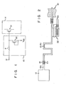
- a basic construction of the MOS type semiconductor device with the gate film protecting circuit will be described referring to Fig. 1.
- a MOS FET Ql constitutes a part of an internal circuit 11.
- a protecting resistor R made of an impurity diffusion layer is inserted between the gate of the MOS FET Q1 and the input terminal (bonding pad) 12.
- a protecting MOS FET Q2 is connected between the gate of the MOS FET Ql and a low potential power source V SS .
- the gate of the MOS FET Q2 is connected to the power source V ss .
- the resistor R and the MOS FET Q2 constitute a protecting circuit 13.
- the over-voltage passes through the resistor R made of an impurity diffusion layer.
- the over-voltage is then clamped by the break down or forward characteristics of the PN junction made between the resistor R and the semiconductor substrate and loses a sharpness in the waveform by the resistivity of the resistor R.
- the high voltage then enters the diffusion layer of the MOS FET Q2 where its amplitude is reduced.
- the reason for this is that as the low potential power source V ss is applied to the gate electrode of the MOS FET Q2, an electric field strength of the surface of the substrate increases to reduce a breakdown voltage. In this way, the amplitude-reduced voltage is applied to the input section of the internal circuit 11, more exactly the gate of the MOS FET Ql, thereby to protect the internal circuit from the extremely high voltage.
- Fig. 2 shows a pattern diagram of the circuit shown in Fig. 1.
- a wiring layer 12a made of aluminum, for example is for connecting the bonding pad 12 as the input terminal and an impurity diffusion layer 15 constituting a protecting resistive layer R.
- An input diffusion layer 14 with a contact hole CH provides a contact of the wiring layer 12a with the resistive layer 15.
- the resistive layer 15 with resistance of approximately 500 ohms to several kilo ohms, has a time constant from 1 ns to 5 ns for the over-voltage. With this time constant, the over-voltage is made gentle in the waveform.
- the thickness of the gate insulation film is thinner and the depth of the diffusion layer is shallower. Because of this reduction of the geometries, the gate protecting circuit is easily broken by a relatively small surge voltage. In this respect, the internal circuit is insatisfactorily protected from the over-voltage.
- an object of the present invention is to provide a further microfabricated MOS type semiconductor device with a gate protecting circuit which can protect the internal circuit from a large surge voltage with a microfabricated structure.
- a MOS type semiconductor device having a gate protecting circuit including an impurity diffusion layer which includes an input section diffusion layer, a circuit other than said gate protecting circuit including, at least, a plurality of impurity diffusion layers having therebetween a first distance equal to or larger than a predetermined minimum distance, and a second distance between said input section layer of said gate protecting circuit and said diffusion layers of said other circuit being determined such that minority carriers emitted from said diffusion layer of one of said circuits do not reach a depletion layer of said diffusion layer of the other of said circuits, the depletion layer being occurred when a surge voltage is applied, and the second distance being also determined to have a value ten times or more said predetermined minimum distance.
- a MOS type semiconductor device comprising a plurality of gate protecting circuits having impurity diffusion layers which include input section diffusion layers, an internal circuit whose input portions being protected by said gate protecting circuits, the internal circuit including a plurality of impurity diffusion layers having therebetween a first distance equal to or larger than a predetermined minimum distance, and second distances between said input section layers of said gate protecting circuits and said diffusion layers of said internal circuit being determined such that minority carriers emitted from said diffusion layers of one of said internal circuit and gate protecting circuits do not reach a depletion layer of said diffusion layers of the other of said internal circuit and gate protecting circuits, the depletion layer being occurred when a surge voltage is applied, the second distances being also limited to have a value ten times or more said predetermined minimum distance, said second distances between said input section layers of said gate protecting circuits and said diffusion layers of said internal circuit being substantially equal to each other.
- Fig. 3 schematically illustrates a pattern of an embodiment of a MOS type semiconductor device according to the present invention.
- Fig. 4 illustrates the details of an internal circuit 22 and a gate protecting circuit 23, in the pattern shown in Fig. 3.
- a semiconductor chip 21 bears an internal circuit 22 containing MOS FETs and a plurality of gate protecting circuits 23 1 , 23 2 , ... formed on the periphery of the internal circuit 22.
- the gate protecting circuits illustrated are only two, for simplicity of illustration.
- the diffusion layers 24, 25, 27 in the internal circuit 22 are arranged separated from each other by minimum distances Dl as determined from a viewpoint of the microfabrication technique and the circuit design.
- the gate protecting circuits 23 1 , 23 2 , ... contain respectively impurity diffusion layers 29 1 , 29 2 , ... forming protecting resistor etc.
- the input terminals (bonding pads) 30 1 , 30 2F ... are provided on the periphery of the chip 21.
- the input terminals 30 1 , 30 2 , ... are connected to gate protecting circuits 23 1 , 23 2 , ... by means of wiring layers 31 1 , 31 2 , ..., respectively.
- Distances from the diffusion layer 29 1 of the gate protecting circuit 23 1 to the diffusion layers 24 to 28 of the internal circuit 22 are selected to such values that minority carriers emitted from the diffusion layers 24 to 28 to the semiconductor substrate do not reach a depletion layer of the diffusion layer 29 1 in the protecting circuit 23 1 , which is caused by a surge voltage applied thereto, and are also selected, though not exactly shown in Figs. 3 and 4, to ten times or more the minimum distances each between the adjacent diffusion layers of those 24 to 28. Though not exactly shown in Figs. 3 and 4, this is correspondingly applied for the distances between the diffusion layer 24 to 28 of the internal circuit 22 and the diffusion layer 29 2 , ... of other respective gate protecting circuits 23 2 , ... and applied for the distance between the diffusion layers 29 1 , 29 2 , ... of adjacent two of the gate protecting circuits 23 1 , 23 2 , ...
- FIG. 5 Further details of the patterns of the diffusion layers 24, 25, 27, 28 of the internal circuit 22 and the gate protecting circuit 23 1 associated therewith are illustrated in Fig. 5.
- the diffusion layer 29 1 of the gate protecting circuit 23 1 contains a contact diffusion layer 29 1 C for making the contact with the input section and a diffusion layer 29 1 R as a resistive layer.
- the contact diffusion layer or input section diffusion layer 29 1 C is connected to the bonding pad 30 1 , through a contact hole CH by way of a wiring layer 31 1 .
- the gate protecting circuit 23 1 further contains an impurity diffusion layer 41.
- a gate electrode 42 made of polysilicon, for example, is formed on the semiconductor chip 21 between the resistive layer 29 1 R and the diffusion layer 41, through a gate insulation film (not shown), for example, an Si0 2 film, and a MOS FET Q12 is formed.
- An electrode layer 43 made of aluminum, for example, is connected to the diffusion layer 41 through a contact hole.
- the electrodes 42 and 43 are both connected to the power source V SS .
- the diffusion layers 24, 25 and gate electrode 44 constitute an input MOS FET Qll.
- the resistive diffusion layer 29 1 R of the gate protecting circuit 23 1 and the gate electrode 44 of the input MOS FET Qll of the internal circuit 22 are interconnected to each other by a wiring layer 45 made of aluminum, for example, through contact holes.
- a P type silicon subtrate 51 is grounded.
- Two N + diffusion regions 52 and 53 with high impurity are formed in the major surface regions of the substrate 51.
- the region 52 is the diffusion layer (typically, an input section i.e., a connecting diffusion layer to a wiring layer extending from a bonding pad) of the gate protecting circuit.
- the region 53 is the diffusion layer of the internal circuit or adjacent gate protecting circuit.
- the region 52 is connected to an input terminal 54.
- the diffusion layer 52 In operation, when a positive surge voltage is applied to the input terminal 54, the diffusion layer 52 is inversely biased or reverse-biased and destroyed, so that a large current flows into a ground point of the substrate 51. In this case, a substrate potential near the diffusion layer 52 rises via a resistance of the substrate 51.
- the diffusion layer 52 in the protecting circuit is located close to the diffusion layer 53 in the internal circuit, the diffusion layer 53 is biased forwardly or forward-biased. Therefore, if the diffusion layer 53 is biased to a fixed potential or its capacitance is large, minority carriers are injected from the diffusion layer 53 into the substrate 51. The minority carriers partially reach the depletion layer 55 where those are accelerated. Since in the depletion layer 55 an intensity of the electric field is high, the minority carriers reaching there receive great energy.
- the minority carriers with the great energy gained hit the silicon crystal in the substrate 51 to generate electron-hole pairs and hence to multiply the carriers.
- the result is to increase a breakdown current largely.
- the break down current causes a great amount of thermal energy to generate at the junction face of the diffusion layer 52, and to destroy the junction face. Therefore, the withstanding voltage is considerably reduced.
- the diffusion layer 53 of the internal circuit is connected to an diffusion layer 61 in another internal circuit separately located, by means of a conductive layer 62 made of aluminum, for example, which is indicated by a single line in Fig. 7.
- a positive surge voltage is applied to the input terminal 54
- the diffusion layer 52 is inversely biased and detroyed.
- the potential of that part of the substrate 51 which is near the diffusion layer 52 rises to forwardly bias the diffusion layer 53 in the near internal circuits.
- the capacitance of the diffusion layer 53 is small, the diffusion layer 53 is supplied with the minority carriers from the diffusion layer 61 because the diffusion layer 53 is connected to the diffusion layer 61, unlike the Fig. 6 case.
- the diffusion layer inversely biased is destroyed, leading to a great reduction of the withstanding voltage.
- the withstanding voltage depends largely on a distance between the diffusion layers of the gate protecting circuit and the diffusion layers the internal circuit or adjacent gate protecting circuit.
- the distances D2 and D3 between the diffusion layers 24 to 28 in the internal circuit 22 and the diffusion layer 29 1 of the gate protecting circuit 23 1 are each set at values at least ten times the minimum distance between the adjacent diffusion layers of those 24 to 28 which are arranged constituting the internal circuit 22.
- This distance must also be such that it perfectly prevents the minority carriers emitted from the diffusion layers 24 to 28 from reaching the depletion layer of the diffusion layer 29 1 in the gate protecting circuit 23 1 which is caused by the impression of the surge voltage.
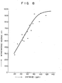
- Fig. 8 shows the result of a destruction test carried out using electric charges storaged in a capacitor of 200 pF.
- a withstanding voltage or tolerance against electro-static discharge On an abscissa is plotted a withstanding voltage or tolerance against electro-static discharge and on an ordinate is plotted a distance (corresponding to D2 shown in Fig. 5) between the input diffusion layer of the gate protecting circuit and the diffusion layer of the internal circuit.
- the graph of Fig. 8 teaches many facts.
- the withstanding voltage depends largely on the distance, and its increase is substantially proportional up to about 100 ⁇ m of the distance.
- the value 400 V at the distance 30 nm is satisfactory in practical use.
- the withstanding voltage is approximately 1000 V.
- the input section diffusion layer 29 1 C is the region to which a surge voltage is first applied, and therefore, the input section diffusion layer 29 1 C is applied with the voltage higher than that applied to the resistor diffusion layer 29 1 R and has a high current density.
- the resistor diffusion layer 29 1 C is less influenced by the surge voltage than the input section diffusion layer 29 1 C is influenced, the resistor diffusion layer 29 1 R is still influenced by the surge voltage. To avoid this influence, it is necessary to set a distance D3 between the resistor diffusion layer and the diffusion layer of the internal circuit by 20 ⁇ m or more.
- the distances between the diffusion layers of the gate protecting circuits 23 1 , 23 2 , ... and the diffusion layers in the internal circuit 22 or adjacent gate protecting circuit are substantially equal to each other.
- the reason for this is that the withstanding voltages in those circuit pairs are set within a narrow range of the variation of the voltages, for the purpose of improving the withstanding voltage of the MOS type semiconductor device as a whole.
- the present invention is not limited to the above-mentioned embodiment.
- any type of the gate protecting circuits can be empolyed in implementing the present invention, if it has a structure containing the diffusion layer.
- the present invention has successfully provided a further microfabricated MOS type semiconductor device with a gate protecting circuit having a high withstanding voltage.
Landscapes
- Metal-Oxide And Bipolar Metal-Oxide Semiconductor Integrated Circuits (AREA)
- Non-Volatile Memory (AREA)
- Protection Of Static Devices (AREA)
- Amplifiers (AREA)
- Semiconductor Integrated Circuits (AREA)
- Insulated Gate Type Field-Effect Transistor (AREA)
Applications Claiming Priority (2)
| Application Number | Priority Date | Filing Date | Title |
|---|---|---|---|
| JP57198191A JPH061833B2 (ja) | 1982-11-11 | 1982-11-11 | Mos形半導体装置 |
| JP198191/82 | 1982-11-11 |
Publications (2)
| Publication Number | Publication Date |
|---|---|
| EP0109070A1 true EP0109070A1 (de) | 1984-05-23 |
| EP0109070B1 EP0109070B1 (de) | 1987-01-28 |
Family
ID=16386982
Family Applications (1)
| Application Number | Title | Priority Date | Filing Date |
|---|---|---|---|
| EP83111291A Expired EP0109070B1 (de) | 1982-11-11 | 1983-11-11 | MOS-Halbleiterbauelement |
Country Status (4)
| Country | Link |
|---|---|
| US (1) | US4688065A (de) |
| EP (1) | EP0109070B1 (de) |
| JP (1) | JPH061833B2 (de) |
| DE (1) | DE3369602D1 (de) |
Cited By (3)
| Publication number | Priority date | Publication date | Assignee | Title |
|---|---|---|---|---|
| EP0670601A3 (de) * | 1994-03-04 | 1995-10-11 | Fuji Electric Co Ltd | |
| EP0722187A3 (de) * | 1995-01-11 | 1996-11-06 | Nec Corp | Integriertes Halbleiterbauelement mit Schutzvorrichtung gegen elektrostatische Entladungen |
| EP0774784A3 (de) * | 1995-11-15 | 2000-07-19 | Nec Corporation | Integrierte Halbleiterschaltungsanordnung mit einem Schutzmittel |
Families Citing this family (8)
| Publication number | Priority date | Publication date | Assignee | Title |
|---|---|---|---|---|
| JPS6271275A (ja) * | 1985-09-25 | 1987-04-01 | Toshiba Corp | 半導体集積回路 |
| JPH0673377B2 (ja) * | 1985-11-27 | 1994-09-14 | 日本電気株式会社 | 入力保護回路 |
| JPH03259561A (ja) * | 1990-03-09 | 1991-11-19 | Fujitsu Ltd | 半導体装置 |
| KR960002094B1 (ko) * | 1990-11-30 | 1996-02-10 | 가부시키가이샤 도시바 | 입력보호회로를 갖춘 반도체장치 |
| JPH07283405A (ja) * | 1994-04-13 | 1995-10-27 | Toshiba Corp | 半導体装置の保護回路 |
| JP3332123B2 (ja) * | 1994-11-10 | 2002-10-07 | 株式会社東芝 | 入力保護回路及びこれを用いた半導体装置 |
| JP2780661B2 (ja) * | 1995-03-04 | 1998-07-30 | 日本電気株式会社 | 半導体装置 |
| KR0145476B1 (ko) * | 1995-04-06 | 1998-08-17 | 김광호 | 칩면적을 줄일 수 있는 패드구조를 가지는 반도체 메모리 장치 |
Citations (2)
| Publication number | Priority date | Publication date | Assignee | Title |
|---|---|---|---|---|
| DE2559360A1 (de) * | 1975-04-03 | 1976-10-14 | Rca Corp | Halbleiterbauteil mit integrierten schaltkreisen |
| JPS5772376A (en) * | 1980-10-24 | 1982-05-06 | Hitachi Ltd | Protective circuit device for semiconductor |
Family Cites Families (16)
| Publication number | Priority date | Publication date | Assignee | Title |
|---|---|---|---|---|
| JPS43455Y1 (de) * | 1964-07-22 | 1968-01-11 | ||
| US3403270A (en) * | 1965-05-10 | 1968-09-24 | Gen Micro Electronics Inc | Overvoltage protective circuit for insulated gate field effect transistor |
| US3407339A (en) * | 1966-05-02 | 1968-10-22 | North American Rockwell | Voltage protection device utilizing a field effect transistor |
| US3413497A (en) * | 1966-07-13 | 1968-11-26 | Hewlett Packard Co | Insulated-gate field effect transistor with electrostatic protection means |
| US3555374A (en) * | 1967-03-03 | 1971-01-12 | Hitachi Ltd | Field effect semiconductor device having a protective diode |
| US4044373A (en) * | 1967-11-13 | 1977-08-23 | Hitachi, Ltd. | IGFET with gate protection diode and antiparasitic isolation means |
| US3601625A (en) * | 1969-06-25 | 1971-08-24 | Texas Instruments Inc | Mosic with protection against voltage surges |
| US4143391A (en) * | 1975-09-12 | 1979-03-06 | Tokyo Shibaura Electric Co., Ltd. | Integrated circuit device |
| JPS5233472B1 (de) * | 1976-07-19 | 1977-08-29 | ||
| JPS5339085A (en) * | 1976-09-22 | 1978-04-10 | Fujitsu Ltd | Protection circuit of semiconductor device |
| JPS54101283A (en) * | 1978-01-27 | 1979-08-09 | Hitachi Ltd | Gate protective device |
| JPS54149479A (en) * | 1978-05-16 | 1979-11-22 | Nec Corp | Semiconductor device |
| JPS55102268A (en) * | 1979-01-31 | 1980-08-05 | Toshiba Corp | Protecting circuit for semiconductor device |
| US4264941A (en) * | 1979-02-14 | 1981-04-28 | National Semiconductor Corporation | Protective circuit for insulated gate field effect transistor integrated circuits |
| JPS56150865A (en) * | 1980-04-25 | 1981-11-21 | Hitachi Ltd | Insulated gate type field effect semiconductor device |
| JPS577969A (en) * | 1980-06-18 | 1982-01-16 | Toshiba Corp | Semiconductor integrated circuit |
-
1982
- 1982-11-11 JP JP57198191A patent/JPH061833B2/ja not_active Expired - Lifetime
-
1983
- 1983-11-11 DE DE8383111291T patent/DE3369602D1/de not_active Expired
- 1983-11-11 EP EP83111291A patent/EP0109070B1/de not_active Expired
-
1986
- 1986-09-04 US US06/903,844 patent/US4688065A/en not_active Expired - Lifetime
Patent Citations (2)
| Publication number | Priority date | Publication date | Assignee | Title |
|---|---|---|---|---|
| DE2559360A1 (de) * | 1975-04-03 | 1976-10-14 | Rca Corp | Halbleiterbauteil mit integrierten schaltkreisen |
| JPS5772376A (en) * | 1980-10-24 | 1982-05-06 | Hitachi Ltd | Protective circuit device for semiconductor |
Non-Patent Citations (1)
| Title |
|---|
| PATENT ABSTRACTS OF JAPAN vol. 006, no. 151 11 August 1982 (1982-08-11) * |
Cited By (6)
| Publication number | Priority date | Publication date | Assignee | Title |
|---|---|---|---|---|
| EP0670601A3 (de) * | 1994-03-04 | 1995-10-11 | Fuji Electric Co Ltd | |
| US5557128A (en) * | 1994-03-04 | 1996-09-17 | Fuji Electric Co., Ltd. | Insulated-gate type bipolar transistor |
| EP0722187A3 (de) * | 1995-01-11 | 1996-11-06 | Nec Corp | Integriertes Halbleiterbauelement mit Schutzvorrichtung gegen elektrostatische Entladungen |
| US5844281A (en) * | 1995-01-11 | 1998-12-01 | Nec Corporation | Semiconductor integrated circuit device with electrostatic protective function |
| CN1055566C (zh) * | 1995-01-11 | 2000-08-16 | 日本电气株式会社 | 半导体器件 |
| EP0774784A3 (de) * | 1995-11-15 | 2000-07-19 | Nec Corporation | Integrierte Halbleiterschaltungsanordnung mit einem Schutzmittel |
Also Published As
| Publication number | Publication date |
|---|---|
| JPS5987873A (ja) | 1984-05-21 |
| DE3369602D1 (en) | 1987-03-05 |
| US4688065A (en) | 1987-08-18 |
| EP0109070B1 (de) | 1987-01-28 |
| JPH061833B2 (ja) | 1994-01-05 |
Similar Documents
| Publication | Publication Date | Title |
|---|---|---|
| US5682047A (en) | Input-output (I/O) structure with capacitively triggered thyristor for electrostatic discharge (ESD) protection | |
| JP2850801B2 (ja) | 半導体素子 | |
| US5270565A (en) | Electro-static discharge protection circuit with bimodal resistance characteristics | |
| US5072273A (en) | Low trigger voltage SCR protection device and structure | |
| US5051860A (en) | Electro-static discharge protection circuit with bimodal resistance characteristics | |
| US5371395A (en) | High voltage input pad protection circuitry | |
| US5291051A (en) | ESD protection for inputs requiring operation beyond supply voltages | |
| EP0109070B1 (de) | MOS-Halbleiterbauelement | |
| EP0215493A1 (de) | Geschützte MOS-Transistorschaltung | |
| US4839768A (en) | Protection of integrated circuits from electrostatic discharges | |
| EP0253105A1 (de) | Integrierte Schaltung mit verbesserter Schutzvorrichtung | |
| US5019883A (en) | Input protective apparatus of semiconductor device | |
| KR100194496B1 (ko) | 반도체 장치 | |
| US6531744B2 (en) | Integrated circuit provided with overvoltage protection and method for manufacture thereof | |
| JP2505652B2 (ja) | 低トリガ電圧scr保護装置及び構造 | |
| US5637887A (en) | Silicon controller rectifier (SCR) with capacitive trigger | |
| EP0202646B1 (de) | Eingangsschutzanordnung | |
| JPS62183184A (ja) | Mos型集積回路 | |
| EP0087155B1 (de) | Mittel zum Verhindern des Durchbruchs einer Isolierschicht in Halbleiteranordnungen | |
| JPS6127916B2 (de) | ||
| JP2537161B2 (ja) | Mos型半導体装置 | |
| EP0198468A2 (de) | Schutzanordnung für eine integrierte Schaltung | |
| US4727405A (en) | Protective network | |
| JPS6221018Y2 (de) | ||
| JPH05505061A (ja) | 電圧ストレス変更可能なesd保護構造 |
Legal Events
| Date | Code | Title | Description |
|---|---|---|---|
| PUAI | Public reference made under article 153(3) epc to a published international application that has entered the european phase |
Free format text: ORIGINAL CODE: 0009012 |
|
| 17P | Request for examination filed |
Effective date: 19831111 |
|
| AK | Designated contracting states |
Designated state(s): DE FR GB IT |
|
| RAP1 | Party data changed (applicant data changed or rights of an application transferred) |
Owner name: KABUSHIKI KAISHA TOSHIBA |
|
| GRAA | (expected) grant |
Free format text: ORIGINAL CODE: 0009210 |
|
| AK | Designated contracting states |
Kind code of ref document: B1 Designated state(s): DE FR GB IT |
|
| ITF | It: translation for a ep patent filed | ||
| ET | Fr: translation filed | ||
| REF | Corresponds to: |
Ref document number: 3369602 Country of ref document: DE Date of ref document: 19870305 |
|
| PLBI | Opposition filed |
Free format text: ORIGINAL CODE: 0009260 |
|
| 26 | Opposition filed |
Opponent name: TELEFUNKEN ELECTRONIC GMBH Effective date: 19871027 |
|
| PLBN | Opposition rejected |
Free format text: ORIGINAL CODE: 0009273 |
|
| STAA | Information on the status of an ep patent application or granted ep patent |
Free format text: STATUS: OPPOSITION REJECTED |
|
| 27O | Opposition rejected |
Effective date: 19890518 |
|
| ITTA | It: last paid annual fee | ||
| PGFP | Annual fee paid to national office [announced via postgrant information from national office to epo] |
Ref country code: GB Payment date: 19971103 Year of fee payment: 15 |
|
| PGFP | Annual fee paid to national office [announced via postgrant information from national office to epo] |
Ref country code: FR Payment date: 19971112 Year of fee payment: 15 |
|
| PGFP | Annual fee paid to national office [announced via postgrant information from national office to epo] |
Ref country code: DE Payment date: 19971114 Year of fee payment: 15 |
|
| PG25 | Lapsed in a contracting state [announced via postgrant information from national office to epo] |
Ref country code: GB Free format text: LAPSE BECAUSE OF NON-PAYMENT OF DUE FEES Effective date: 19981111 |
|
| GBPC | Gb: european patent ceased through non-payment of renewal fee |
Effective date: 19981111 |
|
| PG25 | Lapsed in a contracting state [announced via postgrant information from national office to epo] |
Ref country code: FR Free format text: LAPSE BECAUSE OF NON-PAYMENT OF DUE FEES Effective date: 19990730 |
|
| REG | Reference to a national code |
Ref country code: FR Ref legal event code: ST |
|
| PG25 | Lapsed in a contracting state [announced via postgrant information from national office to epo] |
Ref country code: DE Free format text: LAPSE BECAUSE OF NON-PAYMENT OF DUE FEES Effective date: 19990901 |