EP0113187A2 - Dynamische Halbleiterspeicheranordnung - Google Patents
Dynamische Halbleiterspeicheranordnung Download PDFInfo
- Publication number
- EP0113187A2 EP0113187A2 EP83307270A EP83307270A EP0113187A2 EP 0113187 A2 EP0113187 A2 EP 0113187A2 EP 83307270 A EP83307270 A EP 83307270A EP 83307270 A EP83307270 A EP 83307270A EP 0113187 A2 EP0113187 A2 EP 0113187A2
- Authority
- EP
- European Patent Office
- Prior art keywords
- potential
- resistor
- memory device
- electrodes
- semiconductor memory
- Prior art date
- Legal status (The legal status is an assumption and is not a legal conclusion. Google has not performed a legal analysis and makes no representation as to the accuracy of the status listed.)
- Granted
Links
Images



Classifications
-
- G—PHYSICS
- G11—INFORMATION STORAGE
- G11C—STATIC STORES
- G11C11/00—Digital stores characterised by the use of particular electric or magnetic storage elements; Storage elements therefor
- G11C11/21—Digital stores characterised by the use of particular electric or magnetic storage elements; Storage elements therefor using electric elements
- G11C11/34—Digital stores characterised by the use of particular electric or magnetic storage elements; Storage elements therefor using electric elements using semiconductor devices
- G11C11/40—Digital stores characterised by the use of particular electric or magnetic storage elements; Storage elements therefor using electric elements using semiconductor devices using transistors
- G11C11/401—Digital stores characterised by the use of particular electric or magnetic storage elements; Storage elements therefor using electric elements using semiconductor devices using transistors forming cells needing refreshing or charge regeneration, i.e. dynamic cells
- G11C11/4063—Auxiliary circuits, e.g. for addressing, decoding, driving, writing, sensing or timing
- G11C11/407—Auxiliary circuits, e.g. for addressing, decoding, driving, writing, sensing or timing for memory cells of the field-effect type
- G11C11/4074—Power supply or voltage generation circuits, e.g. bias voltage generators, substrate voltage generators, back-up power, power control circuits
Definitions
- the present invention relates to a dynamic semiconductor memory device, and more particularly to a voltage dividing circuit in a one-transistor one-capacitor dynamic semiconductor memory device.
- a one-transistor one-capacitor dynamic random access memory includes-one metal insulator semiconductor (MIS) transistor and one capacitor for each memory cell.
- the capacitor has one electrode connected to one electrode of the transistor.
- the other electrode of the capacitor (hereinafter referred to as an opposite electrode) was, at the initial stage of the memory of this type, connected to a power supply line or a ground line.
- the opposite electrode tends to be connected to a point having one half of the potential of a power supply potential V CC at the power supply line.
- the reason for connecting the opposite electrode to the point having the potential V cc/ 2 is as follows.
- the area of the electrodes of the capacitor in the memory cell has been more and more decreased.
- the thickness of an insulating film between the electrodes of the capacitor is made thin. Because of the thin insulating film, the tolerance voltage of the insulating film is lowered. Therefore, the voltage applied between the electrodes of the capacitor is preferably small and is set to V CC /2 rather than V CC .
- the present invention starts from such a conventional dynamic RAM as above in which the opposite electrode of the capacitor in each memory cell is connected to the point having the potential V CC /2.
- Two resistors are conventionally used for providing the potential V CC /2. That is, two resistors having the same resistance are connected in series between the power supply line and the ground line so as to provide the potential V CC /2 at the connecting point between the--two resistors, and the opposite electrode of the capacitor in each memory cell is connected to the connecting point between the resistors.
- the potential at the opposite electrode fluctuates in response to internal clock signals or operation of the memory device due to parasitic capacitance in the memory device as described later in detail with reference to the drawings. Consequently read errors often occur, as described later in detail.
- the object of the present invention is to provide such a dynamic semiconductor memory device in which a read error due to the potential fluctuation at the opposite electrode is prevented.
- a dynamic semiconductor memory device comprising a one-transistor one-capacitor dynamic memory cell, a word line, a bit line, and a voltage dividing circuit having a potential-providing terminal for providing an intermediate potential between a power supply potential and a ground potential; the single transistor of the cell having a gate electrode connected to the word line and having two other electrodes; the single capacitor of the cell having a first electrode, which is connected to one of the said other electrodes of the transistor, and an opposite electrode which is operatively connected to the potential-providing terminal of the voltage-dividing circuit; characterized in that the voltage-dividing circuit comprises a potential switching circuit for changing the intermediate potential synchronously with the operation of the memory device.
- the voltage dividing circuit comprises a first resistor and a second resistor connected in series between a power supply line and a ground line and the potential switching circuit in the voltage-dividing circuit comprises a third resistor and a switching transistor having a control electrode for turning on or off the switching transistor and having two other electrodes.
- One end of the third resistor is connected to a connecting point between the first resistor and the second resistor, and the other end of the third resistor is connected to one of the two other electrodes of the switching transistor.
- the other of the two other electrodes of the switching transistor is connected to the ground line or the power supply line, the connecting point being the potential providing terminal.
- the voltage dividing circuit comprises a first resistor and a second resistor connected in series between a power supply line and a ground line, a third resistor and a fourth resistor connected in series between the power supply line and the ground line, a first switching transistor having a first control electrode for turning on or off the first switching transistor and having two other electrodes, and a second switching transistor having a second control electrode for turning on or off the second switching transistor and having two other electrodes.
- One of the two other electrodes of the-first switching transistor is connected to a first connecting point between the first resistor and the second resistor and one of the two other electrodes of the second switching transistor is connected to a second connecting point between the third resistor and the fourth resistor.
- the other of the two other electrodes of the first switching transistor and the other of the two other electrodes of the second switching transistor are commonly connected to the potential-providing terminal.
- the first control electrode operatively receives a first internal clock signal and the second control electrode operatively receives a second-internal clock signal having a phase different by 180° with respect to the phase of the first internal clock signal.
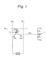
- a conventional dynamic RAM comprises a voltage dividing circuit 1 for providing the potential V CC /2, and a memory cell 2 consisting of a metal-oxide semiconductor (MOS) transistor Q 1 and a capacitor C 1 .
- the gate of the MOS transistor Q 1 is connected to a word line WL 1 .
- One of the other two electrodes (source and drain) of the MOS transistor Q 1 is connected via a node N 1 to one electrode of the capacitor C l .
- the other electrode of the MOS transistor Q 1 is connected to a bit line BL 1 .
- the bit line BL 1 and a bit line BL 1 constitute a bit line pair.
- a sense amplifier SA is connected between the bit lines BL 1 and BL 1 .
- a dummy memory cell (not shown) for storing reference information when the memory cell 2 is to be read is connected to the bit line BL l .
- the voltage dividing circuit 1 consists of two resistors R 1 and R 2 connected in series between a power supply line V CC and a ground line V SS .
- the resistors R 1 and R 2 have the same resistances from each other so that a connecting point N 2 between them provides the potential V CC /2, where V CC is the voltage between the power supply line V CC and the ground line V SS .
- the other electrode (opposite electrode) of the capacitor C 1 and the opposite electrodes of the other capacitors (not shown) in other memory cells are commonly connected to an opposite electrode line OP 1 which is connected to the connecting point N 2 between the resistors R 1 and R 2 . Since the opposite electrode line OP 1 is common to a number of capacitors in the memory cells, it has a considerably large area. Therefore, there are considerably large parasitic capacitances between the opposite electrode line OP 1 and the bit line BL 1 , bit line BL 1 , or the other nodes (not shown). In the figure, only the parasitic capacitances CP 1 and CP 2 are shown for the sake of simplicity, but in practice, there are more parasitic capacitances between the opposite electrode line OP 1 and the other nodes.
- the time constant derived from the resistances (also referred to as R 1 and R 2 ) in the voltage dividing circuit 1 and the parasitic capacitors, for example, CP 1 and CP 2 is preferably as small as possible.
- the resistances R 1 and R 2 are made small for obtaining a small time constant, a considerably large power is consumed in the resistors R 1 and R 2 .
- the resistors R 1 and R 2 are usually made to have high resistances. Because of the high resistances, the time constant is inevitably large.
- FIG. 2A shows waveforms at some points in the dynamic RAM in Fig. 1.
- a row address strobe RAS
- RAS row address strobe
- the dynamic RAM is enabled to effect a read or write operation. More particularly, the dynamic RAM fetches address signals so that the potential of the selected word line WL 1 is raised, in response to the transition from H to L level of the RAS.
- the transistor Q 1 is turned on.
- both of the bit lines BL 1 and BL 1 are precharged to have the potential V CC .
- the capacitor C 1 has been charged up, that is, when the capacitor C 1 is storing a data "1"
- the charges on the bit line BL 1 do not flow through the transistor Q 1 into the capacitor C 1 even after the transistor Q 1 is turned on, so that the potential of the bit line BL 1 is not changed by the rise of the potential of the word line WL 1 , and the charges on the bit line BL 1 flow into the dummy memory cell (not shown) so that the potential of the bit line BL 1 is lowered.
- the sense amplifier SA detects and amplifies the potential difference between the bit lines BL 1 and BL 1 , so that the potential of the bit line BL 1 remains at the V CC and the potential of the bit line BL 1 is lowered to a ground potential V SS .
- the capacitor C 1 is storing a data "0"
- a converse result is obtained.
- the capacitor C 1 is assumed to be storing the data "1".
- the potential of the opposite electrode line OP 1 is boosted to be higher than V CC /2 by a voltage ⁇ V OPH .
- the potential of the opposite electrode line varies in response to the RAS.
- the opposite electrode line OP l Since the opposite electrode line OP l is connected to the node N 2 which provides the constant potential V CC /2, the potential of the opposite electrode line OP 1 will become V CC /2 after a sufficiently long time in the reset interval or in the active interval. This causes a problem, as later described in detail.
- Figure 3A shows the waveforms of the RAS and the potential of the opposite electrode line OP 1 when one of the reset intervals is considerably long.
- the potential of the opposite electrode line OP 1 decreases from V CC /2 + ⁇ V OPH to V CC / 2 during such a long reset interval, as illustrated. Therefore, at the beginning of the active interval followed by the long reset interval, the potential at the opposite electrode line OP 1 is V CC /2 instead of V CC + ⁇ V OPH .
- Figure 3B shows waveforms similar to those in Fig. 2A.
- the difference between Fig. 2A and Fig. 3B is that, in Fig. 3B, the potential of the opposite electrode line OP 1 at the beginning of an active interval is V CC /2 instead of V CC + ⁇ V OPH .
- the potential of the opposite electrode line OP 1 at the beginning of the active interval is V CC /2 + ⁇ V OPH , as is the case of Fig. 2A
- the potential at the node N 1 is V CC .
- the potential of the opposite electrode line OP 1 at the beginning of the active interval is lowered to V CC /2, as shown in Fig.
- the sense amplifier SA erroneously detects that the potential of the bit line BL 1 is lower than the potential of the bit line BL 1 although the capacitor C 1 is storing a data "I".
- the sense amplifier S A amplifies the potential difference between the bit lines BL 1 and BL 1 so that the potential of the bit line BL 1 becomes the ground potential V SS and the potential of the bit line BL 1 becomes the power supply potential V CC . This results in a read error.
- the potential difference between the bit lines BL 1 and BL 1 becomes very small, smaller than, for example, 50 milivolts, so that the sense amplifier, which can detect the potential difference greater than, for example, 50 millivolts may also give a read error operation.
- the waveforms of the bit line BL 1 ' and the opposite electrode line OP 1 ' represent the normal operation shown in Fig. 2A.
- the above described read error in the conventional dynamic RAM is prevented by providing an improved voltage dividing circuit, which outputs V CC / + ⁇ OPH during a reset interval and outputs V CC /2 - ⁇ OPL during an active interval.
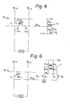
- FIG. 4 is a circuit diagram of a part of a dynamic RAM, according to an embodiment of the present invention.
- the difference between the conventional circuit in Fig. 1 and the circuit in Fig. 4 resides in the voltage dividing circuit. That is, in Fig. 4, a voltage dividing circuit 10 consists of resistors R 10 and R 20 connected in series between the power supply line V CC and the ground line V SS , a resistor R 30 , and a MOS transistor Q 2 .
- the resistor R 30 and the MOS transistor Q 2 ⁇ constitute a potential switching circuit.
- One end of the resistor R 30 is connected to a connecting point N 20 between the resistors R 10 and R 20 .
- the connecting point N 20 is a potential providing terminal of the voltage dividing circuit 10.
- the other end of the resistor R 30 is connected to the drain of the MOS transistor Q 2 .
- the source of the MOS transistor Q 2 is connected to the ground line V SS .
- the gate of the MOS transistor Q 2 operatively receives a clock signal ⁇ A synchronous with the RAS, so that the MOS transistor Q 2 is operatively in an on state during an active interval and is operatively off during a reset interval. That is, the clock signal ⁇ A is a signal in which it is at the H level during an active interval and at the L level during a reset interval.
- This clock signal ⁇ A may be delayed with respect to the RAS by a relatively short period of time if it is negligible as compared to the time constant of the voltage dividing circuit 10. Such a delay is even preferable if it makes the clock isgnal ⁇ A completely synchronous with the change of the potential at the opposite electrode line OP 10 .
- the potential V N20 of the potential providing terminal N 20 is determined only by the resistors R 10 and R 20 i.e.,
- the resistances of the resistors R 10 and R 20 are so determined as to satisfy the following expression (1): where R 10 and R 20 represent the resistances of the resistors R 10 and R 20 , respectively.
- the potential of the opposite electrode line OP 10 is V CC + ⁇ V OPH , as described before in the explanation of the conventional dynamic RAM. Therefore, the potential of the opposite electrode line OP 10 is fixed to V CC /2 + ⁇ V OPH during the reset interval.
- the potential V N20 of the potential providing terminal N 20 is determined by the resistors R 10 , R 20 , and R 30 , i.e., when the resistance of the resistor R 30 is also expressed by R 20 , then, The resistance of the resistor R 30 is so determined as to satisfy the following expression (2):
- the potential of the opposite electrode line OP 10 is V CC - ⁇ V OPL , as described before. Therefore, the potential of the opposite electrode line OP 10 is fixed to V CC /2 - ⁇ V OPL during the active interval.
- the voltages ⁇ V OPH and ⁇ V OPL are experimentally determined.
- Figure 5A shows the waveforms of the RAS, the clock signal ⁇ A and the potential of the opposite electrode line OP 10 when a reset interval is longer than an active interval.
- the potential of the opposite electrode line OP 10 is not decreased from V CC /2 + ⁇ V OPH to V CC /2 but is fixed to V CC /2 + ⁇ V OPH during the reset interval.
- OP 1 represents the potential of the opposite electrode line OP 1 in the conventional dynamic RAM shown in Fig. 1, for easy understanding.
- Figure 5B shows the waveforms of the RAS and the opposite electrode line OP 10 when an active interval is longer than a reset interval.
- the potential of the opposite electrode line OP 10 is not increased from V CC /2 - ⁇ V OPL to V CC /2 but is fixed to V CC /2 - ⁇ V OPL during the reset interval.
- the potential at the node N, , and therefore, at the bit line BL 10 does not change during a sense operation so that a read error is prevented.
- Figure 6 is a circuit diagram of a part of a dynamic RAM, according to another embodiment of the present invention.
- the difference between Fig. 4 and Fig. 6 resides in a voltage dividing circuit 11. That is, in Fig. 6, the voltage dividing circuit 11 comprises resistors R 10 and R 20 connected in series between the power supply line V CC and the ground line V SS , resistors R 31 and R 41 connected in series between the power supply line V CC and the ground line V SS , and two MOS transistors Q 3 and Q 4 .
- the drain of the MOS transistor Q 3 is connected to a connecting point N 30 between the resistors R 10 and R 20
- the drain of the MOS transistor Q 4 is connected to a connecting point N 31 between the resistors R 31 and R 41 .
- the sources of the transistors Q 3 and Q 4 are commonly connected to a potential providing terminal N 32 which is connected to the opposite electrode line OP 20 .
- the gate of the transistor Q 3 operatively receives a clock signal ⁇ B synchronous with the RAS so that the MOS transistor Q 3 is operatively in an on state during a reset interval and is operatively off during an active interval. That is, the clock signal ⁇ B is a signal in which it is at the H level during a reset interval and at the L level during an active interval.
- the gate of the transistor Q 4 operatively receives a clock signal ⁇ C which has a phase different by 180° with respect to the phase of the clock signal ⁇ B . Therefore, the MOS transistor Q 4 is operatively in an on state during an active interval and is operatively in an off state during a reset interval.
- the resistances of the resistors R 10 and R 20 are determined to satisfy the expression (1) described before.
- the resistances.of the resistors R31 and R 41 are determined to satisfy the following expression:
- the potential change at the potential providing terminal N 32 in response to the clock signals ⁇ B and ⁇ C is effected rapidly in comparison with the voltage dividing circuit 10 in Fig. 4.
- the potential providing terminal N 20 is connected through the resistor R 30 to the drain of the transistor Q 2 , and there exists a time constant derived from the resistance R 30 and parasitic capacitances of the MOS transistor Q 2 . Due to the time constant, the rise or fall of the potential of the opposite electrode line OP 10 is slightly delayed, although this delay is negligible.
- Fig. 4 the potential providing terminal N 20 is connected through the resistor R 30 to the drain of the transistor Q 2 , and there exists a time constant derived from the resistance R 30 and parasitic capacitances of the MOS transistor Q 2 . Due to the time constant, the rise or fall of the potential of the opposite electrode line OP 10 is slightly delayed, although this delay is negligible.
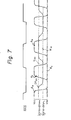
- Fig. 7 illustrates a detailed timing diagram for the clock signals ⁇ B and ⁇ C used in the circuit shown in Fig. 6.
- the potential of the opposite electrode line OP 20 changes between V CC /2 + ⁇ V OPM and V CC /2 - V OPL in the accordance with the operation of the memory device.
- the nodes N 30 and N 31 in the voltage dividing circuit 11 respectively generate the potential V CC /2 + ⁇ V OPH and V CC /2 - ⁇ V OPL , by means of the resistors R 10 and R 20 and, R31 and R 41 .
- the potential of the clock signal ⁇ C is raised to turn on the transistor Q 4 after the potential of the opposite electrode line OP 20 is sufficiently lowered to V CC /2 - ⁇ V OPL . Then the potential of the clock signal ⁇ C is lowered to turn off the transistor Q 4 before the potential of the opposite electrode line OP 20 changes from V CC /2 - ⁇ V OPL .
- the potential of the clock signal ⁇ 3 is raised to turn on the transistor Q 3 after the potential of the opposite electrode line OP 20 sufficiently reach V CC /2 + ⁇ V OPH . Then the potential of the clock signal ⁇ B is lowered to turn off the transistor Q 3 before the potential of the opposite electrode line OP 20 changes.
- the transistors Q 3 and Q 4 are turned on only during intervals in which the potentials of the opposite electrode line OP 2 0 are V CC /2 + ⁇ V OPH and V CC /2 - ⁇ V OPL , respectively.
- the clock signals ⁇ A in Fig. 4, and ⁇ B and ⁇ C in Fig. 6 can be obtained by utilizing internal clock signals in the dynamic RAM which are synchronous with the RAS.
- the resistors R 10 , R 20 ' R 30 ' R 31 , and R 41 themselves in Figs. 4 and 6 are obtained by conventional techniques, that is, by polycrystalline silicon film, by depletion MOS transistors, or by diffusion layers.
- the resistance of each resistor is in an order of, for example, 50 kn.
- the potential of the opposite electrode line OP 10 or OP 20 is substantially kept to V CC /2 + ⁇ V OPH or V CC /2 - ⁇ V OPL during each reset interval or each active interval, respectively.
- the average potential of the opposite electrode line OP 10 or OP 20 for a long period is equal to V CC /2, which is sufficiently low with respect to the tolerance voltage of the capacitor in each memory cell.
- the potential of the opposite electrode line is raised to be higher than V CC /2 at the beginning of each reset interval, and is lowered to be lower than V CC /2 at the beginning of each active interval.
- the present invention is not restricted to the above mentioned case. That is, the opposite electrode line forms parasitic capacitance with various nodes, for example bit lines. Therefore, in response to changes in the potential at those nodes, the potential of the opposite electrode line also fluctuates.
- the present invention is applicable to eliminate malfunctions caused by such fluctuations. Accordingly,the essence of the present invention lies in the design of the voltage dividing circuit shown in Fig. 4 or Fig. 6, in which its output potential is changed in conformity with changes of the potential at the opposite electrode line which is caused by and synchronous with the read or write operation of the device.
Landscapes
- Engineering & Computer Science (AREA)
- Microelectronics & Electronic Packaging (AREA)
- Computer Hardware Design (AREA)
- Dram (AREA)
Applications Claiming Priority (2)
| Application Number | Priority Date | Filing Date | Title |
|---|---|---|---|
| JP211146/82 | 1982-12-01 | ||
| JP57211146A JPS59121691A (ja) | 1982-12-01 | 1982-12-01 | ダイナミツク型半導体記憶装置 |
Publications (3)
| Publication Number | Publication Date |
|---|---|
| EP0113187A2 true EP0113187A2 (de) | 1984-07-11 |
| EP0113187A3 EP0113187A3 (en) | 1986-08-20 |
| EP0113187B1 EP0113187B1 (de) | 1989-03-29 |
Family
ID=16601138
Family Applications (1)
| Application Number | Title | Priority Date | Filing Date |
|---|---|---|---|
| EP83307270A Expired EP0113187B1 (de) | 1982-12-01 | 1983-11-29 | Dynamische Halbleiterspeicheranordnung |
Country Status (4)
| Country | Link |
|---|---|
| US (1) | US4578776A (de) |
| EP (1) | EP0113187B1 (de) |
| JP (1) | JPS59121691A (de) |
| DE (1) | DE3379520D1 (de) |
Cited By (4)
| Publication number | Priority date | Publication date | Assignee | Title |
|---|---|---|---|---|
| US4725985A (en) * | 1983-11-09 | 1988-02-16 | Kabushiki Kaisha Toshiba | Circuit for applying a voltage to a memory cell MOS capacitor of a semiconductor memory device |
| EP0386282A1 (de) * | 1989-03-06 | 1990-09-12 | Siemens Aktiengesellschaft | Integrierte Referenzspannungsquelle |
| US5187685A (en) * | 1985-11-22 | 1993-02-16 | Hitachi, Ltd. | Complementary MISFET voltage generating circuit for a semiconductor memory |
| GB2326763A (en) * | 1997-06-25 | 1998-12-30 | Hyundai Electronics Ind | Semiconductor memory devices |
Families Citing this family (10)
| Publication number | Priority date | Publication date | Assignee | Title |
|---|---|---|---|---|
| JPS61178795A (ja) * | 1985-02-01 | 1986-08-11 | Toshiba Corp | ダイナミツク型半導体記憶装置 |
| JPH0731908B2 (ja) * | 1985-10-09 | 1995-04-10 | 株式会社東芝 | 半導体記憶装置 |
| US4698812A (en) * | 1986-03-03 | 1987-10-06 | Unisys Corporation | Memory system employing a zero DC power gate array for error correction |
| JPS6376192A (ja) * | 1986-09-19 | 1988-04-06 | Fujitsu Ltd | 半導体記憶装置 |
| JPS6376193A (ja) * | 1986-09-19 | 1988-04-06 | Fujitsu Ltd | 半導体記憶装置 |
| JPS6450296A (en) * | 1987-08-21 | 1989-02-27 | Toshiba Corp | Semiconductor integrated circuit device |
| JP2680007B2 (ja) * | 1987-12-04 | 1997-11-19 | 株式会社日立製作所 | 半導体メモリ |
| JPH05342873A (ja) * | 1992-06-10 | 1993-12-24 | Nec Corp | 半導体記憶装置 |
| JP5539916B2 (ja) | 2011-03-04 | 2014-07-02 | ルネサスエレクトロニクス株式会社 | 半導体装置 |
| US10318904B2 (en) | 2016-05-06 | 2019-06-11 | General Electric Company | Computing system to control the use of physical state attainment of assets to meet temporal performance criteria |
Family Cites Families (5)
| Publication number | Priority date | Publication date | Assignee | Title |
|---|---|---|---|---|
| US4240092A (en) * | 1976-09-13 | 1980-12-16 | Texas Instruments Incorporated | Random access memory cell with different capacitor and transistor oxide thickness |
| JPS6044752B2 (ja) * | 1978-04-24 | 1985-10-05 | 日本電気株式会社 | ダイナミツクメモリ |
| US4458336A (en) * | 1980-10-22 | 1984-07-03 | Fujitsu Limited | Semiconductor memory circuit |
| US4482985A (en) * | 1981-04-17 | 1984-11-13 | Hitachi, Ltd. | Semiconductor integrated circuit |
| US4477886A (en) * | 1982-02-26 | 1984-10-16 | Fairchild Camera & Instrument Corporation | Sense/restore circuit for dynamic random access memory |
-
1982
- 1982-12-01 JP JP57211146A patent/JPS59121691A/ja active Granted
-
1983
- 1983-11-28 US US06/555,891 patent/US4578776A/en not_active Expired - Lifetime
- 1983-11-29 EP EP83307270A patent/EP0113187B1/de not_active Expired
- 1983-11-29 DE DE8383307270T patent/DE3379520D1/de not_active Expired
Cited By (7)
| Publication number | Priority date | Publication date | Assignee | Title |
|---|---|---|---|---|
| US4725985A (en) * | 1983-11-09 | 1988-02-16 | Kabushiki Kaisha Toshiba | Circuit for applying a voltage to a memory cell MOS capacitor of a semiconductor memory device |
| US5187685A (en) * | 1985-11-22 | 1993-02-16 | Hitachi, Ltd. | Complementary MISFET voltage generating circuit for a semiconductor memory |
| EP0386282A1 (de) * | 1989-03-06 | 1990-09-12 | Siemens Aktiengesellschaft | Integrierte Referenzspannungsquelle |
| GB2326763A (en) * | 1997-06-25 | 1998-12-30 | Hyundai Electronics Ind | Semiconductor memory devices |
| US6121079A (en) * | 1997-06-25 | 2000-09-19 | Hyundai Electronics Industries, Co., Ltd. | Method for manufacturing a semiconductor memory device |
| US6339240B1 (en) | 1997-06-25 | 2002-01-15 | Hyundai Electronics Industries Co., Ltd. | Semiconductor memory device |
| GB2326763B (en) * | 1997-06-25 | 2002-06-26 | Hyundai Electronics Ind | Semiconductor memory device and method for manufacturing the same |
Also Published As
| Publication number | Publication date |
|---|---|
| JPH0219558B2 (de) | 1990-05-02 |
| DE3379520D1 (en) | 1989-05-03 |
| EP0113187A3 (en) | 1986-08-20 |
| JPS59121691A (ja) | 1984-07-13 |
| US4578776A (en) | 1986-03-25 |
| EP0113187B1 (de) | 1989-03-29 |
Similar Documents
| Publication | Publication Date | Title |
|---|---|---|
| KR0129197B1 (ko) | 메모리셀어레이의 리플레쉬 제어회로 | |
| US5065091A (en) | Semiconductor integrated circuit device testing | |
| KR100377421B1 (ko) | 반도체 기억 장치 | |
| US4475178A (en) | Semiconductor regeneration/precharge device | |
| KR100203344B1 (ko) | 내부 전압의 공급능력이 제어 가능한 반도체 기억장치 | |
| US5523977A (en) | Testing semiconductor memory device having test circuit | |
| JPH04172711A (ja) | 半導体遅延回路 | |
| US6201378B1 (en) | Semiconductor integrated circuit | |
| EP0113187B1 (de) | Dynamische Halbleiterspeicheranordnung | |
| EP0030244A1 (de) | Mos-vorrichtung mit substrat-vormagnetisierungs-erzeugerschaltung | |
| KR930010937B1 (ko) | 셀플레이트 전압발생수단을 갖춘 반도체 기억장치 | |
| US4520466A (en) | Dynamic random access memory | |
| EP0073677B1 (de) | MIS Transistorschaltung mit einer Spannungshalteschaltung | |
| US6628162B2 (en) | Semiconductor integrated circuit | |
| KR930000759B1 (ko) | 다이나믹 메모리 | |
| US4760559A (en) | Semiconductor memory device | |
| US6330173B1 (en) | Semiconductor integrated circuit comprising step-up voltage generation circuit | |
| US4409672A (en) | Dynamic semiconductor memory device | |
| KR0154755B1 (ko) | 가변플레이트전압 발생회로를 구비하는 반도체 메모리장치 | |
| US4875195A (en) | Semiconductor device with a reference voltage generator | |
| US4807193A (en) | Semiconductor memory device with a detection circuit to detect word line potential | |
| JP2685469B2 (ja) | 半導体装置 | |
| EP0790618B1 (de) | Halbleiter-Speicheranordnung, die imstande ist, die Grösse der Substratspannung abhängig vom Zustand zu setzen | |
| US7663952B2 (en) | Capacitor supported precharging of memory digit lines | |
| US6166945A (en) | Method for controlling memory cell having long refresh interval |
Legal Events
| Date | Code | Title | Description |
|---|---|---|---|
| PUAI | Public reference made under article 153(3) epc to a published international application that has entered the european phase |
Free format text: ORIGINAL CODE: 0009012 |
|
| AK | Designated contracting states |
Designated state(s): DE FR GB |
|
| PUAL | Search report despatched |
Free format text: ORIGINAL CODE: 0009013 |
|
| AK | Designated contracting states |
Kind code of ref document: A3 Designated state(s): DE FR GB |
|
| 17P | Request for examination filed |
Effective date: 19861029 |
|
| 17Q | First examination report despatched |
Effective date: 19871125 |
|
| GRAA | (expected) grant |
Free format text: ORIGINAL CODE: 0009210 |
|
| AK | Designated contracting states |
Kind code of ref document: B1 Designated state(s): DE FR GB |
|
| REF | Corresponds to: |
Ref document number: 3379520 Country of ref document: DE Date of ref document: 19890503 |
|
| ET | Fr: translation filed | ||
| PLBE | No opposition filed within time limit |
Free format text: ORIGINAL CODE: 0009261 |
|
| STAA | Information on the status of an ep patent application or granted ep patent |
Free format text: STATUS: NO OPPOSITION FILED WITHIN TIME LIMIT |
|
| 26N | No opposition filed | ||
| PGFP | Annual fee paid to national office [announced via postgrant information from national office to epo] |
Ref country code: FR Payment date: 20001110 Year of fee payment: 18 |
|
| PGFP | Annual fee paid to national office [announced via postgrant information from national office to epo] |
Ref country code: DE Payment date: 20001120 Year of fee payment: 18 |
|
| PGFP | Annual fee paid to national office [announced via postgrant information from national office to epo] |
Ref country code: GB Payment date: 20001129 Year of fee payment: 18 |
|
| PG25 | Lapsed in a contracting state [announced via postgrant information from national office to epo] |
Ref country code: GB Free format text: LAPSE BECAUSE OF NON-PAYMENT OF DUE FEES Effective date: 20011129 |
|
| REG | Reference to a national code |
Ref country code: GB Ref legal event code: IF02 |
|
| PG25 | Lapsed in a contracting state [announced via postgrant information from national office to epo] |
Ref country code: DE Free format text: LAPSE BECAUSE OF NON-PAYMENT OF DUE FEES Effective date: 20020702 |
|
| GBPC | Gb: european patent ceased through non-payment of renewal fee |
Effective date: 20011129 |
|
| PG25 | Lapsed in a contracting state [announced via postgrant information from national office to epo] |
Ref country code: FR Free format text: LAPSE BECAUSE OF NON-PAYMENT OF DUE FEES Effective date: 20020730 |
|
| REG | Reference to a national code |
Ref country code: FR Ref legal event code: ST |
|
| REG | Reference to a national code |
Ref country code: FR Ref legal event code: ST |