EP0113820A2 - Verfahren und Vorrichtung zum Einbetten eines Drahtes in einem lichthärtbaren Klebstoff - Google Patents
Verfahren und Vorrichtung zum Einbetten eines Drahtes in einem lichthärtbaren Klebstoff Download PDFInfo
- Publication number
- EP0113820A2 EP0113820A2 EP83110963A EP83110963A EP0113820A2 EP 0113820 A2 EP0113820 A2 EP 0113820A2 EP 83110963 A EP83110963 A EP 83110963A EP 83110963 A EP83110963 A EP 83110963A EP 0113820 A2 EP0113820 A2 EP 0113820A2
- Authority
- EP
- European Patent Office
- Prior art keywords
- wire
- photocurable adhesive
- layer
- softened
- laminate sheet
- Prior art date
- Legal status (The legal status is an assumption and is not a legal conclusion. Google has not performed a legal analysis and makes no representation as to the accuracy of the status listed.)
- Granted
Links
Images
Classifications
-
- H—ELECTRICITY
- H05—ELECTRIC TECHNIQUES NOT OTHERWISE PROVIDED FOR
- H05K—PRINTED CIRCUITS; CASINGS OR CONSTRUCTIONAL DETAILS OF ELECTRIC APPARATUS; MANUFACTURE OF ASSEMBLAGES OF ELECTRICAL COMPONENTS
- H05K3/00—Apparatus or processes for manufacturing printed circuits
- H05K3/10—Apparatus or processes for manufacturing printed circuits in which conductive material is applied to the insulating support in such a manner as to form the desired conductive pattern
- H05K3/103—Apparatus or processes for manufacturing printed circuits in which conductive material is applied to the insulating support in such a manner as to form the desired conductive pattern by bonding or embedding conductive wires or strips
-
- H—ELECTRICITY
- H05—ELECTRIC TECHNIQUES NOT OTHERWISE PROVIDED FOR
- H05K—PRINTED CIRCUITS; CASINGS OR CONSTRUCTIONAL DETAILS OF ELECTRIC APPARATUS; MANUFACTURE OF ASSEMBLAGES OF ELECTRICAL COMPONENTS
- H05K7/00—Constructional details common to different types of electric apparatus
- H05K7/02—Arrangements of circuit components or wiring on supporting structure
- H05K7/06—Arrangements of circuit components or wiring on supporting structure on insulating boards, e.g. wiring harnesses
-
- H—ELECTRICITY
- H05—ELECTRIC TECHNIQUES NOT OTHERWISE PROVIDED FOR
- H05K—PRINTED CIRCUITS; CASINGS OR CONSTRUCTIONAL DETAILS OF ELECTRIC APPARATUS; MANUFACTURE OF ASSEMBLAGES OF ELECTRICAL COMPONENTS
- H05K2201/00—Indexing scheme relating to printed circuits covered by H05K1/00
- H05K2201/10—Details of components or other objects attached to or integrated in a printed circuit board
- H05K2201/10227—Other objects, e.g. metallic pieces
- H05K2201/10287—Metal wires as connectors or conductors
-
- H—ELECTRICITY
- H05—ELECTRIC TECHNIQUES NOT OTHERWISE PROVIDED FOR
- H05K—PRINTED CIRCUITS; CASINGS OR CONSTRUCTIONAL DETAILS OF ELECTRIC APPARATUS; MANUFACTURE OF ASSEMBLAGES OF ELECTRICAL COMPONENTS
- H05K2203/00—Indexing scheme relating to apparatus or processes for manufacturing printed circuits covered by H05K3/00
- H05K2203/11—Treatments characterised by their effect, e.g. heating, cooling, roughening
- H05K2203/1105—Heating or thermal processing not related to soldering, firing, curing or laminating, e.g. for shaping the substrate or during finish plating
-
- H—ELECTRICITY
- H05—ELECTRIC TECHNIQUES NOT OTHERWISE PROVIDED FOR
- H05K—PRINTED CIRCUITS; CASINGS OR CONSTRUCTIONAL DETAILS OF ELECTRIC APPARATUS; MANUFACTURE OF ASSEMBLAGES OF ELECTRICAL COMPONENTS
- H05K3/00—Apparatus or processes for manufacturing printed circuits
- H05K3/38—Improvement of the adhesion between the insulating substrate and the metal
- H05K3/386—Improvement of the adhesion between the insulating substrate and the metal by the use of an organic polymeric bonding layer, e.g. adhesive
Definitions
- This invention relates to a method and apparatus for embedding wire in an adhesive layer on a laminate sheet used in the manufacture of circuit boards.
- Encapsulated wire circuit boards are typically fabricated by embedding wires in a layer of adhesive on a sheet of laminate material. Depending on the particular circuit board desired, the wires may be embedded on one or both sides of the laminate sheet. If a multilayer circuit board is desired, then several sheets of laminate material containing wires embedded thereon may be bonded together.
- wires tend to move in the adhesive from the time they are laid on the sheet until the time that the adhesive is cured.
- wire connections between layers on a multilayer circuit board or even those on a single layered board may not be made. This necessitates repairing the board and in some cases scrapping the board altogether.
- the wire connection problem has been observed in low density wired boards as well as high density wired boards.
- This invention achieves the above objects by providing a method and apparatus for embedding wires in a photocurable adhesive on a laminate sheet wherein the position integrity of the wires is maintained.
- wire is laid in a predetermined pattern in a layer of uncured malleable photocurable adhesive.
- the photocurable adhesive surrounding the just laid wire is either partially cured or totally cured. In this manner, the wire is fixed in place and unable to move out of its predetermined position.
- the uncured layer of photocurable adhesive may be heated and thus softened, prior to wire laying, by using either ultrasonic energy, optical energy, or some combination of the two. Additionally, the entire layer of the photo curable adhesive may be heated at the same time or selected areas on the layer may be heated as the wire is being laid.
- a beam of ultraviolet radiation from a laser is used to cure the photocurable adhesive.
- a fiber optic cable may be connected to the laser in order to provide greater control over the directionality of the laser beam.
- the photocurable adhesive is only partially cured as the wires are laid on the laminate sheet. This partial curing keeps the wires in the position that they were laid in. After all of the wires have been laid on a sheet, the sheet is then placed in an apparatus which scans an ultraviolet beam across the entire sheet. In this manner, the photocurable adhesive is totally cured and the wires are permanently fixed on the laminate sheet.
- This two step curing process would typically be used to prevent cracking of the adhesive when a multitude of wires are to be laid and/or when wire cross-overs are required.
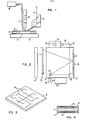
- Laminate sheet 11 is clamped onto movable base 13.
- Laminate sheet 11 is typically constructed of a fiber glass type material.
- a layer of photocurable adhesive 12 is placed on the surface of laminate sheet 11.
- Figs. 1 and 4 show a layer of adhesive 12 on both sides of laminate sheet 11, the layer of photocurable adhesive 12 may be placed on just one side of laminate sheet 11.
- the layer of photocurable adhesive 12 is typically in sheet form having a thickness of 0,127 - 0,254 mm (5-10 mils) with plastic wrapping on both sides.
- the wrapping from one side of photocurable adhesive 12 is first removed.
- Adhesive 12 is then placed wrapper-less side down onto laminate sheet 11 and hot-pressed thereto. The wrapping on the other side is not removed until it is desired to lay wire 14 on laminate sheet 11.
- wire may be laid according to the desired pattern.
- Wire 14 is fed from a wheel (not shown) and set into photocurable adhesive 12 using machine head 15 and stylus 16.
- Machine head 15 guides wire 14 over the desired pattern.
- Machine head 15 may be automatically controlled, such as, for example, by a microprocessor controller.
- An example of a wiring pattern is shown in Fig. 3.
- Stylus 16 vibrates up and down very quickly as it pushes down on wire 14 as it is being laid out over the desired pattern. Stylus 16 serves two functions. First, the very quick up and down vibratory motion produces ultrasonic heating. This ultrasonic heating softens the adhesive layer 12 in the vicinity of the wire 14 being laid. The second function of stylus 16 is to push wire 14 down into the heated, softened layer of photocurable adhesive 12. Fig. 4 shows the position of wire 14 in adhesive layer 12.
- stylus 16 with its ultrasonic heating may be used for pushing wire 14 down into adhesive 12.
- an optical heating means for softening adhesive 12 in conjunction with a roller for pushing wire 14 down into photocurable adhesive 12 may be employed.
- an optical heating means used in conjunction with stylus 16 can also be used.
- an optical source of energy for heating the entire sheet at once may be used either with a roller or with a vibrating stylus.
- Fiber optic cable 17 guides a beam of ultraviolet radiation from laser 18 onto the photocurable adhesive 12 around wire 14 as the wire is being laid.
- a xenon chloride laser (XeCl) operating at a wavelength of 360-370 nm may be used.
- Fiber optic cable 17, stylus 16, and machine head 15 are stationary with respect to one another. Their movement across laminate sheet 11, which is clamped to base 13, is at an approximate speed of 5,08 m/min (200 inches per minute). Head 15, stylus 16, and cable 17 are mounted on a bridge (not shown) which moves in one direction across the base 13 and which also rotates angularly with respect to the base 13. Base 13 moves in a direction orthogonal to the direction of motion of the bridge. Using the nomenclature associated with a Cartesian coordinate system, it can be said that the bridge moves in the X and & directions, while the base moves in the Y direction. It will be recognized by those skilled in the art that the directions of movement of base and bridge may be reversed or that either one may be held fixed while the other moves in the X, Y and 9 directions.
- the preferred embodiment entails a two step curing process.
- the first, or partial curing step has already been described.
- the second and final step will now be described in relation to Fig. 2.
- the entire laminate sheet 11 is placed into laser curing apparatus 35.
- the laminate sheet 11 containing the wired pattern in the partially cured adhesive is secured to clamp member 21.
- a beam 34 of ultraviolet radiation from laser 29 is then scanned across the secured laminate sheet 11 so as to totally cure photocurable adhesive 12, thus permanently embedding the wired pattern into the adhesive layer on the laminate sheet 11.
- Optical apparatus 32 contains precision optically flat mirrors 22, 24, 25, and 23. These mirrors are situated in optical apparatus 32 so as to reflect beam 34 from laser 29 onto laminate sheet 11.
- Disc-shaped mirror 25 is connected via shaft 27 to motor 26.
- Motor 26 controls the position of mirror 25 so that beam 34 may be scanned from the top of the laminate sheet to the bottom of the laminate sheet in predetermined increments.
- the width of beam 34 from laser 29 is on the order of 1,6 mm (1/16 inch).
- mirror 25 is moved so that beam 34 is scanned over the entire length of sheet 11.
- Motor control means 28 is used to control the operation of motor 26.
- a microprocessor may be used, for example, as motor control means 28.
- Beam 34 is moved from left to right across the width of sheet 11 with the aid of stepper motor 31 which is connected to laser 29. Beam 34 begins at the top left corner of laminate sheet 11. Stepper motor 31 steps laser 29 from left to right thus causing beam 34 to step across laminate sheet 11 from left to right. When beam 34 gets to the right hand edge of sheet 11, the stepper motor is reset to the far left position and mirror 25 rotates so as to move beam 34 a beam width - in this example, it is 1,6 mm (1/16 inch) - down the sheet 11. This step and rotate cycle continues until beam 34 has scanned across the entire laminate sheet 11. It must be emphasized that beam 34 does not scan individual wires on sheet 11 but rather scans across the entire sheet. If a pattern has been wired on both sides of laminate sheet 11, then the sheet must be turned over and the process completed for the opposite side. Beam absorber 33 functions as a safety device, shielding an operator of the apparatus from stray ultraviolet radiation.
Landscapes
- Engineering & Computer Science (AREA)
- Microelectronics & Electronic Packaging (AREA)
- Manufacturing & Machinery (AREA)
- Manufacturing Of Printed Wiring (AREA)
- Adhesives Or Adhesive Processes (AREA)
- Production Of Multi-Layered Print Wiring Board (AREA)
Applications Claiming Priority (2)
| Application Number | Priority Date | Filing Date | Title |
|---|---|---|---|
| US45216182A | 1982-12-22 | 1982-12-22 | |
| US452161 | 1982-12-22 |
Publications (3)
| Publication Number | Publication Date |
|---|---|
| EP0113820A2 true EP0113820A2 (de) | 1984-07-25 |
| EP0113820A3 EP0113820A3 (en) | 1984-09-12 |
| EP0113820B1 EP0113820B1 (de) | 1987-09-09 |
Family
ID=23795307
Family Applications (1)
| Application Number | Title | Priority Date | Filing Date |
|---|---|---|---|
| EP19830110963 Expired EP0113820B1 (de) | 1982-12-22 | 1983-11-03 | Verfahren und Vorrichtung zum Einbetten eines Drahtes in einem lichthärtbaren Klebstoff |
Country Status (3)
| Country | Link |
|---|---|
| EP (1) | EP0113820B1 (de) |
| JP (1) | JPS59121992A (de) |
| DE (1) | DE3373610D1 (de) |
Cited By (9)
| Publication number | Priority date | Publication date | Assignee | Title |
|---|---|---|---|---|
| FR2585210A1 (fr) * | 1985-07-19 | 1987-01-23 | Kollmorgen Tech Corp | Procede de fabrication de plaquettes a circuits d'interconnexion |
| FR2585209A1 (fr) * | 1985-07-19 | 1987-01-23 | Kollmorgen Tech Corp | Plaquettes a circuits traces par fil et leur procede de fabrication |
| US4693778A (en) * | 1985-07-19 | 1987-09-15 | Kollmorgen Technologies Corporation | Apparatus for making scribed circuit boards and circuit board modifications |
| AT385624B (de) * | 1981-04-14 | 1988-04-25 | Kollmorgen Tech Corp | Verfahren zum herstellen eines mit einem verbindungsnetzwerk versehenen bauteils |
| US4859807A (en) * | 1985-07-19 | 1989-08-22 | Kollmorgen Technologies Corporation | Wire scribed circuit boards and method of manufacture |
| WO1999067693A1 (en) * | 1998-06-22 | 1999-12-29 | Niilo Kaartinen | Freeze valve |
| GB2391115A (en) * | 2002-07-19 | 2004-01-28 | Agilent Technologies Inc | Printed circuit board with track formed by conductive tape |
| US20150145815A1 (en) * | 2012-05-31 | 2015-05-28 | Zytronic Displays Limited | Multi-touch sensing arrangement |
| US10078402B2 (en) | 2012-05-31 | 2018-09-18 | Zytronic Displays Limited | Touch sensitive displays |
Families Citing this family (2)
| Publication number | Priority date | Publication date | Assignee | Title |
|---|---|---|---|---|
| JPH0436955U (de) * | 1990-07-26 | 1992-03-27 | ||
| JP5907369B2 (ja) * | 2011-09-29 | 2016-04-26 | 日立化成株式会社 | 布線装置及びこれを用いたマルチワイヤ配線板の製造方法 |
Family Cites Families (3)
| Publication number | Priority date | Publication date | Assignee | Title |
|---|---|---|---|---|
| US3674914A (en) * | 1968-02-09 | 1972-07-04 | Photocircuits Corp | Wire scribed circuit boards and method of manufacture |
| US4500389A (en) * | 1981-04-14 | 1985-02-19 | Kollmorgen Technologies Corporation | Process for the manufacture of substrates to interconnect electronic components |
| IT1171559B (it) * | 1981-09-29 | 1987-06-10 | Gd Spa | Dispositivo ribaltatore per articoli a forma di barretta in particolare sigarette |
-
1983
- 1983-11-03 DE DE8383110963T patent/DE3373610D1/de not_active Expired
- 1983-11-03 EP EP19830110963 patent/EP0113820B1/de not_active Expired
- 1983-11-18 JP JP21637483A patent/JPS59121992A/ja active Granted
Cited By (17)
| Publication number | Priority date | Publication date | Assignee | Title |
|---|---|---|---|---|
| AT385624B (de) * | 1981-04-14 | 1988-04-25 | Kollmorgen Tech Corp | Verfahren zum herstellen eines mit einem verbindungsnetzwerk versehenen bauteils |
| US4859807A (en) * | 1985-07-19 | 1989-08-22 | Kollmorgen Technologies Corporation | Wire scribed circuit boards and method of manufacture |
| FR2585210A1 (fr) * | 1985-07-19 | 1987-01-23 | Kollmorgen Tech Corp | Procede de fabrication de plaquettes a circuits d'interconnexion |
| US4693778A (en) * | 1985-07-19 | 1987-09-15 | Kollmorgen Technologies Corporation | Apparatus for making scribed circuit boards and circuit board modifications |
| US4711026A (en) * | 1985-07-19 | 1987-12-08 | Kollmorgen Technologies Corporation | Method of making wires scribed circuit boards |
| FR2585209A1 (fr) * | 1985-07-19 | 1987-01-23 | Kollmorgen Tech Corp | Plaquettes a circuits traces par fil et leur procede de fabrication |
| EP0217019A3 (en) * | 1985-07-19 | 1988-08-10 | Kollmorgen Technologies Corporation | Method of manufacturing interconnection circuit boards |
| EP0212227A3 (en) * | 1985-07-19 | 1987-05-13 | Kollmorgen Technologies Corporation | Process for the manufacture of wire scribed circuit boards and articles produced thereby |
| GB2180696B (en) * | 1985-07-19 | 1989-07-19 | Kollmorgen Tech Corp | Process for the manufacture of wire scribed circuit boards and articles produced thereby |
| AU594352B2 (en) * | 1985-07-19 | 1990-03-08 | Advanced Interconnection Technology, Inc. | Wire scribed circuit boards and method of manufacture |
| WO1999067693A1 (en) * | 1998-06-22 | 1999-12-29 | Niilo Kaartinen | Freeze valve |
| US6311713B1 (en) | 1998-06-22 | 2001-11-06 | Niilo Kaartinen | Freeze valve |
| GB2391115A (en) * | 2002-07-19 | 2004-01-28 | Agilent Technologies Inc | Printed circuit board with track formed by conductive tape |
| US6825679B2 (en) | 2002-07-19 | 2004-11-30 | Agilent Technologies, Inc. | Electrically conductive structure and method for implementing circuit changes on printed circuit boards |
| GB2391115B (en) * | 2002-07-19 | 2005-08-31 | Agilent Technologies Inc | Electrically conductive structure and method for implementing circuit changes on printed circuit boards |
| US20150145815A1 (en) * | 2012-05-31 | 2015-05-28 | Zytronic Displays Limited | Multi-touch sensing arrangement |
| US10078402B2 (en) | 2012-05-31 | 2018-09-18 | Zytronic Displays Limited | Touch sensitive displays |
Also Published As
| Publication number | Publication date |
|---|---|
| EP0113820B1 (de) | 1987-09-09 |
| DE3373610D1 (en) | 1987-10-15 |
| EP0113820A3 (en) | 1984-09-12 |
| JPH0133958B2 (de) | 1989-07-17 |
| JPS59121992A (ja) | 1984-07-14 |
Similar Documents
| Publication | Publication Date | Title |
|---|---|---|
| JP7154809B2 (ja) | ウエーハの加工方法 | |
| EP0113820B1 (de) | Verfahren und Vorrichtung zum Einbetten eines Drahtes in einem lichthärtbaren Klebstoff | |
| CN110391182B (zh) | 晶片的加工方法 | |
| KR100332939B1 (ko) | 광조형장치 및 방법 | |
| CN107108317A (zh) | 用于对玻璃制品的边缘进行密封的方法和设备 | |
| KR20030055083A (ko) | 프리프레그의 제조방법 | |
| TWI881961B (zh) | 雷射加工裝置 | |
| JP3233060B2 (ja) | 樹脂製品のレーザ加工方法 | |
| JP3660741B2 (ja) | 電子回路装置の製造方法 | |
| KR102660540B1 (ko) | 절삭 블레이드의 정형 방법 | |
| JP7088768B2 (ja) | ウェーハの分割方法 | |
| KR20210028650A (ko) | 레이저 가공 장치, 레이저 가공 방법 및 성막 마스크 제조 방법 | |
| JP2003311831A (ja) | 凹凸パターンの形成方法 | |
| JPS61116322A (ja) | 立体形状形成装置 | |
| JPS63141725A (ja) | 立体形状形成装置 | |
| US5873511A (en) | Apparatus and method for forming solder bonding pads | |
| CN106414016A (zh) | 用于粘接剂活化的使用光的加热装置及其在预成型装置中的集成 | |
| JP2861321B2 (ja) | 立体形状物の形成方法 | |
| CN115255655A (zh) | 晶片的加工方法和激光加工装置 | |
| JP7851739B2 (ja) | ウエーハの加工方法 | |
| JP2527021B2 (ja) | 光学的造形法 | |
| JPH05269864A (ja) | 三次元光造形装置 | |
| JPH058306A (ja) | 光学的造形法 | |
| JP3314608B2 (ja) | 光造型方法 | |
| JPH0518751U (ja) | レーザ加熱装置 |
Legal Events
| Date | Code | Title | Description |
|---|---|---|---|
| PUAI | Public reference made under article 153(3) epc to a published international application that has entered the european phase |
Free format text: ORIGINAL CODE: 0009012 |
|
| PUAL | Search report despatched |
Free format text: ORIGINAL CODE: 0009013 |
|
| AK | Designated contracting states |
Designated state(s): DE FR GB |
|
| AK | Designated contracting states |
Designated state(s): DE FR GB |
|
| 17P | Request for examination filed |
Effective date: 19841029 |
|
| 17Q | First examination report despatched |
Effective date: 19860424 |
|
| D17Q | First examination report despatched (deleted) | ||
| GRAA | (expected) grant |
Free format text: ORIGINAL CODE: 0009210 |
|
| AK | Designated contracting states |
Kind code of ref document: B1 Designated state(s): DE FR GB |
|
| REF | Corresponds to: |
Ref document number: 3373610 Country of ref document: DE Date of ref document: 19871015 |
|
| ET | Fr: translation filed | ||
| PLBE | No opposition filed within time limit |
Free format text: ORIGINAL CODE: 0009261 |
|
| STAA | Information on the status of an ep patent application or granted ep patent |
Free format text: STATUS: NO OPPOSITION FILED WITHIN TIME LIMIT |
|
| 26N | No opposition filed | ||
| PGFP | Annual fee paid to national office [announced via postgrant information from national office to epo] |
Ref country code: GB Payment date: 19921027 Year of fee payment: 10 |
|
| PGFP | Annual fee paid to national office [announced via postgrant information from national office to epo] |
Ref country code: FR Payment date: 19921029 Year of fee payment: 10 |
|
| PGFP | Annual fee paid to national office [announced via postgrant information from national office to epo] |
Ref country code: DE Payment date: 19921121 Year of fee payment: 10 |
|
| PG25 | Lapsed in a contracting state [announced via postgrant information from national office to epo] |
Ref country code: GB Effective date: 19931103 |
|
| GBPC | Gb: european patent ceased through non-payment of renewal fee |
Effective date: 19931103 |
|
| PG25 | Lapsed in a contracting state [announced via postgrant information from national office to epo] |
Ref country code: FR Effective date: 19940729 |
|
| PG25 | Lapsed in a contracting state [announced via postgrant information from national office to epo] |
Ref country code: DE Effective date: 19940802 |
|
| REG | Reference to a national code |
Ref country code: FR Ref legal event code: ST |