EP0114076A2 - Magnetkopf - Google Patents
Magnetkopf Download PDFInfo
- Publication number
- EP0114076A2 EP0114076A2 EP84100437A EP84100437A EP0114076A2 EP 0114076 A2 EP0114076 A2 EP 0114076A2 EP 84100437 A EP84100437 A EP 84100437A EP 84100437 A EP84100437 A EP 84100437A EP 0114076 A2 EP0114076 A2 EP 0114076A2
- Authority
- EP
- European Patent Office
- Prior art keywords
- magnetic
- magnetic film
- film
- films
- laminated
- Prior art date
- Legal status (The legal status is an assumption and is not a legal conclusion. Google has not performed a legal analysis and makes no representation as to the accuracy of the status listed.)
- Granted
Links
- XEEYBQQBJWHFJM-UHFFFAOYSA-N Iron Chemical compound [Fe] XEEYBQQBJWHFJM-UHFFFAOYSA-N 0.000 claims abstract description 36
- PXHVJJICTQNCMI-UHFFFAOYSA-N Nickel Chemical compound [Ni] PXHVJJICTQNCMI-UHFFFAOYSA-N 0.000 claims abstract description 28
- 230000006698 induction Effects 0.000 claims abstract description 20
- 229910001004 magnetic alloy Inorganic materials 0.000 claims abstract description 20
- 229910052742 iron Inorganic materials 0.000 claims abstract description 18
- 239000010941 cobalt Substances 0.000 claims abstract description 15
- GUTLYIVDDKVIGB-UHFFFAOYSA-N cobalt atom Chemical compound [Co] GUTLYIVDDKVIGB-UHFFFAOYSA-N 0.000 claims abstract description 15
- 229910017052 cobalt Inorganic materials 0.000 claims abstract description 14
- 229910000640 Fe alloy Inorganic materials 0.000 claims abstract description 12
- 239000000470 constituent Substances 0.000 claims abstract description 10
- 239000000696 magnetic material Substances 0.000 claims abstract description 9
- 229910000990 Ni alloy Inorganic materials 0.000 claims abstract description 8
- 229910045601 alloy Inorganic materials 0.000 claims description 13
- 239000000956 alloy Substances 0.000 claims description 13
- VYPSYNLAJGMNEJ-UHFFFAOYSA-N Silicium dioxide Chemical compound O=[Si]=O VYPSYNLAJGMNEJ-UHFFFAOYSA-N 0.000 claims description 7
- 239000000203 mixture Substances 0.000 claims description 6
- 229910052751 metal Inorganic materials 0.000 claims description 2
- 239000002184 metal Substances 0.000 claims description 2
- TWNQGVIAIRXVLR-UHFFFAOYSA-N oxo(oxoalumanyloxy)alumane Chemical compound O=[Al]O[Al]=O TWNQGVIAIRXVLR-UHFFFAOYSA-N 0.000 claims 1
- 239000004065 semiconductor Substances 0.000 claims 1
- 229910052814 silicon oxide Inorganic materials 0.000 claims 1
- 239000010408 film Substances 0.000 description 223
- 239000000758 substrate Substances 0.000 description 15
- 238000004544 sputter deposition Methods 0.000 description 14
- 230000035699 permeability Effects 0.000 description 12
- 230000005415 magnetization Effects 0.000 description 10
- 230000015572 biosynthetic process Effects 0.000 description 8
- 229910000889 permalloy Inorganic materials 0.000 description 7
- 239000002356 single layer Substances 0.000 description 7
- XUIMIQQOPSSXEZ-UHFFFAOYSA-N Silicon Chemical compound [Si] XUIMIQQOPSSXEZ-UHFFFAOYSA-N 0.000 description 6
- 230000000694 effects Effects 0.000 description 6
- 239000000463 material Substances 0.000 description 6
- 229910052759 nickel Inorganic materials 0.000 description 6
- 229910052710 silicon Inorganic materials 0.000 description 6
- 239000010703 silicon Substances 0.000 description 6
- XKRFYHLGVUSROY-UHFFFAOYSA-N Argon Chemical compound [Ar] XKRFYHLGVUSROY-UHFFFAOYSA-N 0.000 description 4
- 229910000676 Si alloy Inorganic materials 0.000 description 4
- 229910052681 coesite Inorganic materials 0.000 description 4
- 229910052906 cristobalite Inorganic materials 0.000 description 4
- 229910052682 stishovite Inorganic materials 0.000 description 4
- 239000010409 thin film Substances 0.000 description 4
- 229910052905 tridymite Inorganic materials 0.000 description 4
- 230000002411 adverse Effects 0.000 description 3
- 238000002425 crystallisation Methods 0.000 description 3
- 230000008025 crystallization Effects 0.000 description 3
- 230000007423 decrease Effects 0.000 description 3
- 239000007789 gas Substances 0.000 description 3
- ZOXJGFHDIHLPTG-UHFFFAOYSA-N Boron Chemical compound [B] ZOXJGFHDIHLPTG-UHFFFAOYSA-N 0.000 description 2
- UQSXHKLRYXJYBZ-UHFFFAOYSA-N Iron oxide Chemical compound [Fe]=O UQSXHKLRYXJYBZ-UHFFFAOYSA-N 0.000 description 2
- ZOKXTWBITQBERF-UHFFFAOYSA-N Molybdenum Chemical compound [Mo] ZOKXTWBITQBERF-UHFFFAOYSA-N 0.000 description 2
- RTAQQCXQSZGOHL-UHFFFAOYSA-N Titanium Chemical compound [Ti] RTAQQCXQSZGOHL-UHFFFAOYSA-N 0.000 description 2
- 239000000654 additive Substances 0.000 description 2
- 229910052782 aluminium Inorganic materials 0.000 description 2
- XAGFODPZIPBFFR-UHFFFAOYSA-N aluminium Chemical compound [Al] XAGFODPZIPBFFR-UHFFFAOYSA-N 0.000 description 2
- 229910052786 argon Inorganic materials 0.000 description 2
- 229910052796 boron Inorganic materials 0.000 description 2
- 238000010586 diagram Methods 0.000 description 2
- 238000010292 electrical insulation Methods 0.000 description 2
- 239000011521 glass Substances 0.000 description 2
- 239000011810 insulating material Substances 0.000 description 2
- 238000000034 method Methods 0.000 description 2
- 229910052750 molybdenum Inorganic materials 0.000 description 2
- 239000011733 molybdenum Substances 0.000 description 2
- 238000002360 preparation method Methods 0.000 description 2
- 238000001552 radio frequency sputter deposition Methods 0.000 description 2
- 239000000377 silicon dioxide Substances 0.000 description 2
- 125000006850 spacer group Chemical group 0.000 description 2
- 229910052719 titanium Inorganic materials 0.000 description 2
- 239000010936 titanium Substances 0.000 description 2
- VYZAMTAEIAYCRO-UHFFFAOYSA-N Chromium Chemical compound [Cr] VYZAMTAEIAYCRO-UHFFFAOYSA-N 0.000 description 1
- 229910000531 Co alloy Inorganic materials 0.000 description 1
- OAICVXFJPJFONN-UHFFFAOYSA-N Phosphorus Chemical compound [P] OAICVXFJPJFONN-UHFFFAOYSA-N 0.000 description 1
- ATJFFYVFTNAWJD-UHFFFAOYSA-N Tin Chemical compound [Sn] ATJFFYVFTNAWJD-UHFFFAOYSA-N 0.000 description 1
- QCWXUUIWCKQGHC-UHFFFAOYSA-N Zirconium Chemical compound [Zr] QCWXUUIWCKQGHC-UHFFFAOYSA-N 0.000 description 1
- 230000000996 additive effect Effects 0.000 description 1
- QVGXLLKOCUKJST-UHFFFAOYSA-N atomic oxygen Chemical compound [O] QVGXLLKOCUKJST-UHFFFAOYSA-N 0.000 description 1
- 230000015556 catabolic process Effects 0.000 description 1
- 229910052804 chromium Inorganic materials 0.000 description 1
- 239000011651 chromium Substances 0.000 description 1
- 239000004020 conductor Substances 0.000 description 1
- 238000005260 corrosion Methods 0.000 description 1
- 230000007797 corrosion Effects 0.000 description 1
- 230000008878 coupling Effects 0.000 description 1
- 238000010168 coupling process Methods 0.000 description 1
- 238000005859 coupling reaction Methods 0.000 description 1
- 238000006731 degradation reaction Methods 0.000 description 1
- 239000012535 impurity Substances 0.000 description 1
- 238000009413 insulation Methods 0.000 description 1
- 239000011229 interlayer Substances 0.000 description 1
- 238000007733 ion plating Methods 0.000 description 1
- 230000001788 irregular Effects 0.000 description 1
- 238000010030 laminating Methods 0.000 description 1
- 238000003475 lamination Methods 0.000 description 1
- 230000005389 magnetism Effects 0.000 description 1
- 238000012986 modification Methods 0.000 description 1
- 230000004048 modification Effects 0.000 description 1
- 229910052758 niobium Inorganic materials 0.000 description 1
- 239000010955 niobium Substances 0.000 description 1
- GUCVJGMIXFAOAE-UHFFFAOYSA-N niobium atom Chemical compound [Nb] GUCVJGMIXFAOAE-UHFFFAOYSA-N 0.000 description 1
- 230000001151 other effect Effects 0.000 description 1
- 239000001301 oxygen Substances 0.000 description 1
- 229910052760 oxygen Inorganic materials 0.000 description 1
- 229910052698 phosphorus Inorganic materials 0.000 description 1
- 239000011574 phosphorus Substances 0.000 description 1
- 238000007747 plating Methods 0.000 description 1
- 239000000843 powder Substances 0.000 description 1
- 238000000926 separation method Methods 0.000 description 1
- 229910052718 tin Inorganic materials 0.000 description 1
- -1 titanum Chemical compound 0.000 description 1
- WFKWXMTUELFFGS-UHFFFAOYSA-N tungsten Chemical compound [W] WFKWXMTUELFFGS-UHFFFAOYSA-N 0.000 description 1
- 229910052721 tungsten Inorganic materials 0.000 description 1
- 239000010937 tungsten Substances 0.000 description 1
- 238000007738 vacuum evaporation Methods 0.000 description 1
- 229910052720 vanadium Inorganic materials 0.000 description 1
- LEONUFNNVUYDNQ-UHFFFAOYSA-N vanadium atom Chemical compound [V] LEONUFNNVUYDNQ-UHFFFAOYSA-N 0.000 description 1
- 238000004804 winding Methods 0.000 description 1
- 229910052726 zirconium Inorganic materials 0.000 description 1
Images


Classifications
-
- G—PHYSICS
- G11—INFORMATION STORAGE
- G11B—INFORMATION STORAGE BASED ON RELATIVE MOVEMENT BETWEEN RECORD CARRIER AND TRANSDUCER
- G11B5/00—Recording by magnetisation or demagnetisation of a record carrier; Reproducing by magnetic means; Record carriers therefor
- G11B5/127—Structure or manufacture of heads, e.g. inductive
- G11B5/31—Structure or manufacture of heads, e.g. inductive using thin films
- G11B5/3109—Details
- G11B5/3113—Details for improving the magnetic domain structure or avoiding the formation or displacement of undesirable magnetic domains
-
- G—PHYSICS
- G11—INFORMATION STORAGE
- G11B—INFORMATION STORAGE BASED ON RELATIVE MOVEMENT BETWEEN RECORD CARRIER AND TRANSDUCER
- G11B5/00—Recording by magnetisation or demagnetisation of a record carrier; Reproducing by magnetic means; Record carriers therefor
- G11B5/127—Structure or manufacture of heads, e.g. inductive
- G11B5/147—Structure or manufacture of heads, e.g. inductive with cores being composed of metal sheets, i.e. laminated cores with cores composed of isolated magnetic layers, e.g. sheets
-
- H—ELECTRICITY
- H01—ELECTRIC ELEMENTS
- H01F—MAGNETS; INDUCTANCES; TRANSFORMERS; SELECTION OF MATERIALS FOR THEIR MAGNETIC PROPERTIES
- H01F10/00—Thin magnetic films, e.g. of one-domain structure
-
- Y—GENERAL TAGGING OF NEW TECHNOLOGICAL DEVELOPMENTS; GENERAL TAGGING OF CROSS-SECTIONAL TECHNOLOGIES SPANNING OVER SEVERAL SECTIONS OF THE IPC; TECHNICAL SUBJECTS COVERED BY FORMER USPC CROSS-REFERENCE ART COLLECTIONS [XRACs] AND DIGESTS
- Y10—TECHNICAL SUBJECTS COVERED BY FORMER USPC
- Y10S—TECHNICAL SUBJECTS COVERED BY FORMER USPC CROSS-REFERENCE ART COLLECTIONS [XRACs] AND DIGESTS
- Y10S428/00—Stock material or miscellaneous articles
- Y10S428/922—Static electricity metal bleed-off metallic stock
- Y10S428/923—Physical dimension
- Y10S428/924—Composite
- Y10S428/926—Thickness of individual layer specified
-
- Y—GENERAL TAGGING OF NEW TECHNOLOGICAL DEVELOPMENTS; GENERAL TAGGING OF CROSS-SECTIONAL TECHNOLOGIES SPANNING OVER SEVERAL SECTIONS OF THE IPC; TECHNICAL SUBJECTS COVERED BY FORMER USPC CROSS-REFERENCE ART COLLECTIONS [XRACs] AND DIGESTS
- Y10—TECHNICAL SUBJECTS COVERED BY FORMER USPC
- Y10S—TECHNICAL SUBJECTS COVERED BY FORMER USPC CROSS-REFERENCE ART COLLECTIONS [XRACs] AND DIGESTS
- Y10S428/00—Stock material or miscellaneous articles
- Y10S428/922—Static electricity metal bleed-off metallic stock
- Y10S428/9265—Special properties
- Y10S428/928—Magnetic property
-
- Y—GENERAL TAGGING OF NEW TECHNOLOGICAL DEVELOPMENTS; GENERAL TAGGING OF CROSS-SECTIONAL TECHNOLOGIES SPANNING OVER SEVERAL SECTIONS OF THE IPC; TECHNICAL SUBJECTS COVERED BY FORMER USPC CROSS-REFERENCE ART COLLECTIONS [XRACs] AND DIGESTS
- Y10—TECHNICAL SUBJECTS COVERED BY FORMER USPC
- Y10T—TECHNICAL SUBJECTS COVERED BY FORMER US CLASSIFICATION
- Y10T428/00—Stock material or miscellaneous articles
- Y10T428/11—Magnetic recording head
- Y10T428/1107—Magnetoresistive
- Y10T428/1121—Multilayer
- Y10T428/1129—Super lattice [e.g., giant magneto resistance [GMR] or colossal magneto resistance [CMR], etc.]
-
- Y—GENERAL TAGGING OF NEW TECHNOLOGICAL DEVELOPMENTS; GENERAL TAGGING OF CROSS-SECTIONAL TECHNOLOGIES SPANNING OVER SEVERAL SECTIONS OF THE IPC; TECHNICAL SUBJECTS COVERED BY FORMER USPC CROSS-REFERENCE ART COLLECTIONS [XRACs] AND DIGESTS
- Y10—TECHNICAL SUBJECTS COVERED BY FORMER USPC
- Y10T—TECHNICAL SUBJECTS COVERED BY FORMER US CLASSIFICATION
- Y10T428/00—Stock material or miscellaneous articles
- Y10T428/12—All metal or with adjacent metals
- Y10T428/12493—Composite; i.e., plural, adjacent, spatially distinct metal components [e.g., layers, joint, etc.]
- Y10T428/12535—Composite; i.e., plural, adjacent, spatially distinct metal components [e.g., layers, joint, etc.] with additional, spatially distinct nonmetal component
- Y10T428/12611—Oxide-containing component
-
- Y—GENERAL TAGGING OF NEW TECHNOLOGICAL DEVELOPMENTS; GENERAL TAGGING OF CROSS-SECTIONAL TECHNOLOGIES SPANNING OVER SEVERAL SECTIONS OF THE IPC; TECHNICAL SUBJECTS COVERED BY FORMER USPC CROSS-REFERENCE ART COLLECTIONS [XRACs] AND DIGESTS
- Y10—TECHNICAL SUBJECTS COVERED BY FORMER USPC
- Y10T—TECHNICAL SUBJECTS COVERED BY FORMER US CLASSIFICATION
- Y10T428/00—Stock material or miscellaneous articles
- Y10T428/12—All metal or with adjacent metals
- Y10T428/12493—Composite; i.e., plural, adjacent, spatially distinct metal components [e.g., layers, joint, etc.]
- Y10T428/12632—Four or more distinct components with alternate recurrence of each type component
-
- Y—GENERAL TAGGING OF NEW TECHNOLOGICAL DEVELOPMENTS; GENERAL TAGGING OF CROSS-SECTIONAL TECHNOLOGIES SPANNING OVER SEVERAL SECTIONS OF THE IPC; TECHNICAL SUBJECTS COVERED BY FORMER USPC CROSS-REFERENCE ART COLLECTIONS [XRACs] AND DIGESTS
- Y10—TECHNICAL SUBJECTS COVERED BY FORMER USPC
- Y10T—TECHNICAL SUBJECTS COVERED BY FORMER US CLASSIFICATION
- Y10T428/00—Stock material or miscellaneous articles
- Y10T428/12—All metal or with adjacent metals
- Y10T428/12493—Composite; i.e., plural, adjacent, spatially distinct metal components [e.g., layers, joint, etc.]
- Y10T428/12771—Transition metal-base component
- Y10T428/12861—Group VIII or IB metal-base component
- Y10T428/12931—Co-, Fe-, or Ni-base components, alternative to each other
-
- Y—GENERAL TAGGING OF NEW TECHNOLOGICAL DEVELOPMENTS; GENERAL TAGGING OF CROSS-SECTIONAL TECHNOLOGIES SPANNING OVER SEVERAL SECTIONS OF THE IPC; TECHNICAL SUBJECTS COVERED BY FORMER USPC CROSS-REFERENCE ART COLLECTIONS [XRACs] AND DIGESTS
- Y10—TECHNICAL SUBJECTS COVERED BY FORMER USPC
- Y10T—TECHNICAL SUBJECTS COVERED BY FORMER US CLASSIFICATION
- Y10T428/00—Stock material or miscellaneous articles
- Y10T428/12—All metal or with adjacent metals
- Y10T428/12493—Composite; i.e., plural, adjacent, spatially distinct metal components [e.g., layers, joint, etc.]
- Y10T428/12771—Transition metal-base component
- Y10T428/12861—Group VIII or IB metal-base component
- Y10T428/12937—Co- or Ni-base component next to Fe-base component
Definitions
- This invention relates to a magnetic film structure having high saturation magnetic induction and low coercive force so as to provide good results when used for a magnetic head core especially of the type which has performance suitable for high density magnetic recording.
- a metal powder tape has been developed which can facilitate attainment of a higher coercive force Hc of 1,200 to 1,600 Oe than a coercive force of 600 to 700 Oe of a conventional iron oxide power tape.
- a magnetic head is required which is made of a magnetic material having a high saturation magnetic induction.
- a magnetic material of an alloy containing iron, cobalt or nickel as principal constituent can easily be prepared, having a high saturation magnetic induction of 10,000 gauss or more.
- the laminated magnetic film structure is prepared by so-called thin film formation technique such as sputtering, vacuum evaporation, ion plating or plating.
- Fig. 1 shows a prior art laminated magnetic film structure.
- This known laminated structure is prepared by alternate and successive formation of magnetic films 10 and non-magnetic insulating films 11 on a non-magnetic insulating substrate 13.
- Each of the magnetic films 10 has a thickness of several microns and each of the non-magnetic insulating films 11 has a thickness which is about 1/10 of the thickness of the magnetic film 10.
- the crystalline metallic magnetic film behaves itself like a columnar structure as shown at 12 in Fig. 1, it is difficult for magnetization to move through the boundary of the columnar structure and hence the laminated structure exhibits a large coercive force.
- a magnetic head prepared with the magnetic films of such a.large coercive force there arises a problem that a magnetic head core is magnetized when a large external magnetic field is applied thereto.
- An approach to this problem is such that magnetic film of a thickness of submicrons and non-magnetic films of about 1,000 A thickness are alternately laminated to thereby reduce the coercive force.
- an about 1 U m thickness single layer film of an alloy of iron and 6.5 weight % silicon (hereinafter, weight % will be simply referred to as %) prepared by sputtering has a coercive force of several oersteds
- the laminated structure according to the above proposal can reduce the coercive force to about 1 Oe.
- a minimum coercive force obtained with this proposed structure will however be 0.8 Oe and for this reason, the proposed structure is sometimes unsatisfactory for the magnetic head material.
- An object of this invention is to provide a magnetic film structure having a high saturation magnetic induction and a lower coercive force than that of the prior art structure.
- Another object of this invention is to provide a magnetic film structure for use in a magnetic head which can exhibit an excellent recording and reproducing characteristic in relation to a high coercive force recording medium.
- Still another object of this invention is to provide a laminated magnetic film structure comprised of laminated magnetic films of high saturation magnetic induction which can exhibit low coercive force and high permeability.
- crystalline metallic magnetic films having a high saturation magnetic induction of 10,000 gauss or more are used for easy formation of a magnetic film structure having a low coercive force which can not be obtained from the prior art laminated magnetic film structure in which magnetic films and non-magnetic insulating films are laminated alternately.
- the inventors of the present application have found that such a magnetic film structure can be materialized by replacing the non-magnetic insulating intermediate film interposed between adjacent main magnetic films in the prior art laminated magnetic film structure with magnetic intermediate film different from the main magnetic film.
- the magnetic intermediate film is preferably made of a magnetic material having a relatively low coercive force (less than 10 Oe) and a low magnetostriction (less than 1 0 6) .
- a plurality of main magnetic films of a predetermined thickness made of a metallic magnetic alloy having high saturation magnetic induction and low magnetostriction are laminated through intermediate magnetic films of a predetermined thickness made of a magnetic material different from that of the main magnetic films.
- Fig. 2 shows, in sectional form, a magnetic film structure according to this invention.
- the magnetic film structure comprises main magnetic films 20 made of a magnetic alloy containing, for example, iron or cobalt as principal constituent and having a high saturation magnetic induction, intermediate magnetic films 21 made of an alloy having relatively low coercive force and magnetostriction, for example, a nickel and iron alloy (permalloy) or amorphous magnetic alloy, and a non-magnetic substrate 23.
- the magnetization which is otherwise oriented in a direction vertical to the film surface along the columnar structure and the magnetization which is also otherwise difficult to move through the boundary of the columnar structure are both oriented to the interior of the film so as to have ability to move within the film under the application of a small magnetic field, thereby reducing the coercive force.
- the intermediate magnetic films 21 presumably assist in aiding the magnetic coupling between the respective main magnetic films 20 to enhance the movement of the magnetization.
- the main magnetic film of this invention be made of either a magnetic alloy containing iron as principal constituent and one or more elements selected from a group of silicon, aluminum and titanium by 1 to 30% in total or a magnetic alloy containing cobalt as principal constituent and one or more elements selected from a group of iron, vanadium, titanium and tin.
- Either alloy has a low magnetostriction (less than 10-6) and a high saturation magnetic induction (more than 10,000 gauss). If the magnetostriction exceeds 10 -6 , the magnetic characteristic disadvantageously will become increasingly irregular under the application of stress and if the saturation magnetic induction is not greater than 10,000 gauss, satisfactory recording on a medium of large coercive force will disadvantageously be prevented.
- the alloy composition of the main magnetic film may be added with an additive by less than 10%.
- the main magnetic film preferably has a saturation magnetic induction of more than 10,000 gauss and a coercive force of less than 10 Oe.
- the intermediate magnetic film made of a nickel and iron alloy (permalloy) or amorphous magnetic alloy preferably has an alloy composition which exhibits a low coercive force (less than 10 Oe) and a low magnetostriction (less than 10- 6 ).
- the magnetic material of the intermediate magnetic film is different from that of the main magnetic film, namely, the former material contains an element as principal constituent different from that of the latter material or has an atomic configuration different from that of the latter material, attainment of effects of the present invention can be expected. If the same alloy is used for both the intermediate and main magnetic films, the columnar structure of the intermediate magnetic film and that of the main magnetic film are linked together and good results can not be obtained.
- the amorphous magnetic alloy is free from this problem and preferably employed in the present invention.
- the thickness of the intermediate magnetic film is selected to a value which can substantially eliminate the influence of its coercive force upon the laminated magnetic film structure.
- the intermediate magnetic film having a low coercive force (less than 10 Oe) and a thickness of 30 0 to 500 A as described above a fine structure of multilayer magnetic films can be realized relatively easily.
- the thickness of the intermediate magnetic film be 10 to 80 A.
- the magnetic film structure of the present invention preferably has a laminated structure comprising a plurality of main magnetic films containing iron or cobalt as principal constituent and having a high saturation magnetic induction, and intermediate magnetic films made of a nickel and iron alloy or amorphous magnetic alloy and each interposed between adjacent main magnetic films.
- the present invention can effectively improve a crystalline magnetic film structure in which the magnetic film exhibits the columnar (or needle-like) structure when it takes the form of a single-layer film.
- the coercive force can be reduced by about one order by applying teachings of the present invention to a magnetic film structure in which the magnetic film in the form of a single layer has a coercive force of the order of several oersteds.
- the thickness of each main magnetic film ranges from 0.05 ⁇ m to 0.5 ⁇ m, most preferably, 0.05 ⁇ m to 0.3 ⁇ m.
- the thickness being less than 0.05 ⁇ m, the magnetic characteristic of the intermediate magnetic film comes out and if the intermediate magnetic film is reduced in thickness, film homogeneity will be impared to prevent realization of a stable fine structure.
- the thickness being more than 0.5 ⁇ m, the influence of the columnar structure becomes predominant to increase the coercive force.
- the thickness of each intermediate magnetic film ranges from 30 A to 500 A, most preferably, 50 A to 300 A when the intermediate magnetic film is made of the nickel and iron alloy or amorphous magnetic alloy, having a coercive force of 10 Oe or less.
- the intermediate magnetic film preferably o 0 has a thickness which ranges from 10 A to 80 A, most 0 0 preferably, 15 A to 70 A when it is made of a material having a relatively high coercive force such as cobalt.
- the laminated magnetic film structure of the present invention wherein the main magnetic films and the intermediate magnetic films are laminated as described previously can provide a lower coercive force than that of the prior art laminated magnetic film structure wherein the main magnetic films and the non-magnetic insulating intermediate films are laminated.
- the intermediate magnetic film is made of a nickel and iron alloy having a magnetostriction of 1 x 10 -6 or less which contains, for example, about 81% nickel and about 91% iron.
- the intermediate magnetic film is made of an amorphous magnetic alloy, it is preferable that, for example, cobalt be added with one or more elements selected from a group of zirconium, titanum, molybdenum, niobium, tungsten, aluminum, nickel, chromium, silicon and boron or cobalt, iron and nickel be added with silicon, boron and phosphorus, respectively, to provide a coercive force of several oersteds or less.
- cobalt be added with one or more elements selected from a group of zirconium, titanum, molybdenum, niobium, tungsten, aluminum, nickel, chromium, silicon and boron or cobalt, iron and nickel be added with silicon, boron and phosphorus, respectively, to provide a coerc
- the crystallization temperature is desired to be high.
- the prepared laminated magnetic film structure is affected by the excessive coercive force, making it difficult to obtain a low coercive force.
- the number of laminated main magnetic films and intermediate magnetic films is determined in accordance with the thickness of the laminated magnetic film structure adapted for utilization and purpose of the structure and the thus determined number cooperates with the thickness of each film to provide an intended characteristic.
- a thick laminated magnetic film structure having excellent high frequency magnetic properties can also be materialized by laminating a predetermined number of laminated magnetic film units of a suitable thickness each comprised of the main magnetic films and intermediate magnetic films through non-magnetic insulating films such as SiO 2 films or Al 2 0 3 films having electrical insulation.
- the number of the laminated films in the laminated magnetic film unit and the number of the laminated magnetic film units in the thick laminated magnetic film structure are determined in accordance with the thickness of the thick laminated magnetic film structure adapted for utilization and purpose of the structure and the thus determined number cooperates with the thickness of the main magnetic film, intermediate magnetic film and non-magnetic insulating film to provide an intended characteristic.
- the non-magnetic insulating film normally has a thickness which ranges from 0.05 ⁇ m to 1 um. For the thickness being more than 1 ⁇ m, the magnetic properties such as permeability are degraded whereas for the thickness being less than 0.05 ⁇ m, the formation.of a complete film becomes difficult, resulting in insufficient interlayer insulation.
- Each of the laminated magnetic film units to be laminated through the non-magnetic insulating films normally has 10 to 50 main magnetic films which are laminated through the intermediate magnetic films. Preferably, about 30 main magnetic films are used to obtain a thick laminated magnetic film structure having excellent high frequency magnetic properties.
- Electrodes 31, 32 and 33 are target electrodes (cathodes).
- An alloy target containing iron or cobalt as principal constituent for formation of the main magnetic film is disposed on the electrode 31
- an alloy target made of an nickel and iron alloy (permalloy) or amorphous magnetic alloy for formation of the intermediate magnetic film is disposed on the electrode 32
- a target made of an insulating material such as Si0 2 or A1 2 0 3 for formation of the non-magnetic insulating film is disposed on the electrode 33.
- Electrodes 34, 35 and 36 respectively provided directly beneath the electrodes 31, 32 and 33 are substrate electrodes (anodes).
- a specimen 37 may be carried on any one of the substrate electrodes as necessary.
- a magnetic field may be applied in parallel to the surface of the specimen 37 by means of electromagnets 38 and 38' during sputtering so that the direction of easy magnetization of the magnetic film structure to be formed may be oriented in parallel to the surface of the film.
- Electric discharge is effected within an atmosphere of argon gas which is introduced into the vacuum container 30 via a gas inlet pipe 39.
- An evacuation pipe 40 is provided for the vacuum container 30, and a switch 41 is adapted to switch the electrodes.
- a single layer film of 1.5 ⁇ m thickness thus formed on the non-magnetic substrate has magnetic properties including a coercive force Hc of 2.5 Oe, a permeability p of 400 at 5 MHz, and a saturation magnetic induction of 18,500 gauss.
- Sputtering is effected under the application of a magnetic field (about 10 Oe) oriented in one direction parallel to the surface of the magnetic film. These magnetic properties are measured in the direction of hard magnetization which is vertical to the surface of the magnetic film.
- a glass substrate is used as the non-magnetic substrate. Of various conditions for sputtering, the silicon content in the targe must be excessive since the composition in a resulting sputtered film tends to shift to the iron content in comparison with the composition in the target.
- the coercive force Hc tends to decrease.
- the substrate temperature is preferably above 250°C to mitigate stress in the film.
- the coercive force tends to become low but in consideration of stability of electric discharge during sputtering, the distance is preferably about 20 to 30 mm.
- the vacuum container is highly evacuated to a vacuum degree of the order of 10 Torr prior to the introduction of argon gas since the remaining oxygen and impurity will adversely affect the magnetic properties of the magnetic film structure.
- the intermediate magnetic film is prepared by RF sputtering under the following conditions.
- a thus prepared intermediate magnetic film approximately has a composition of 81% nickel and 19% iron.
- a laminated magnetic film structure having 15 laminated main magnetic films is thus prepared, having a total thickness of about 1.5 ⁇ m with each of the main magnetic films formed in 0.1 ⁇ m thickness and each of the inter-0 mediate magnetic films formed in 100 A thickness.
- Another intermediate magnetic film is prepared by using an amorphous magnetic alloy under the following conditions.
- an intermediate magnetic film of SiO 2 or molybdenum is also prepared.
- the substrate temperature is set to 250°C during sputtering of the main magnetic films.
- Table 1 shows magnetic properties of the laminated magnetic film structure having the thus prepared main magnetic films of iron and 6.5% silicon alloy and various kinds of intermediate magnetic films as listed in Table 1. Magnetic properties of a plurality of structures immediately after sputtering are averaged and indicated in Table 1. Item (a) represents properties of single layer films of iron and 6.5% silicon alloy, items (b) and (c) represent properties of laminated magnetic film structures having the prior art non-magnetic insulating intermediate films, and items (d) to (h) represent properties of laminated magnetic film structures having intermediate magnetic films of permalloy or amorphous magnetic alloy according to teachings of the present invention.
- the laminated magnetic film structures having the intermediate magnetic films according to the invention have an extremely lower coercive force than that of the prior art laminated magnetic film structures having the non-magnetic insulating intermediate films.
- the coercive force is reduced to below 0.5 Oe to provide a practically significant permeability.
- each of the main magnetic films can have a thickness which ranges from 0.05 ⁇ m to 0.5 ⁇ m to ensure that the columnar structure can be sectionalized to an extent that the magnetic properties of the laminated magnetic film structure are not affected adversely.
- Fig. 4 shows the relation between the thickness of the intermediate film or spacer, coercive force Hc and permeability ⁇ at 5 MHz when the main magnetic film of iron and 6.5% silicon alloy has a thickness of 0.1 ⁇ m and the intermediate magnetic film is made of permalloy.
- the laminated magnetic film structure has 15 main magnetic films and the intermediate magnetic films interposed between adjacent main magnetic films. It will be seen from Fig. 4 that the coercive force is about 0.8 Oe for the thickness of the intermediate magnetic film which ranges from 30 A to 500 A, is less than 0.5 Oe for the thickness range of 50 to 300 A and is minimum near 100 A.
- the permeability becomes maximum 0 near 100 A.
- the range for preferable coercive force substantially coincides with the range for preferable permeability.
- the thickness being less than 30 A, the magnetic properties of the intermediate magnetic film are diluted to increase the coercive force whereas for the thickness 0 being less than 10 A, it is difficult to block the columnar structure in the main magnetic film, allowing the columnar structure to grow, whereby the effects of the present invention are degraded.
- the magnetic properties of the intermediate magnetic film comes out to increase the coercive force and decrease the saturation magnetic induction of the main magnetic film even when the main magnetic film inherently has a high saturation magnetic induction. Since the thickness of the intermediate magnetic film is difficult to directly measure, it is calculated from theoretical sputtering rate when the alloy is deposited to a thickness of several microns and controlled in terms of time.
- the thickness can be set to a range which is relatively easy to control, bringing out significant, practical effects.
- a magnetic field is applied in one direction parallel to the surface of the main magnetic film during sputtering so that the direction of easy magnetization is established which coincides with the direction of the applied magnetic field.
- the permeability represented by curve 51
- the permeability represented by curve 52
- the latter permeability is higher than the former. Accordingly, in a magnetic head incorporating the laminated magnetic film structure of the present invention, its direction of hard magnetization can be arranged in an advantageous direction with respect to a magnetic circuit for the magnetic head.
- a resulting single layer structure exhibits a coercive force of several of tens of oersteds whereas a resulting structure according to the present invention exhibits a coercive force which is reduced to 1 Oe or less. Since the cobalt and iron alloy inherently has a high coercive force, the film thickness needs to be reduced slightly.
- the main magnetic film used in the present invention is made of the magnetic alloy which contains iron or cobalt as principal constituent and has a high saturation magnetic induction (more than 10,000 gauss) and a magnetostriction of nearly zero.
- the present invention can reduce the coercive force, thereby providing a laminated magnetic film structure suitable for use in a magnetic head.
- Fig. 6 shows still another example of the film structure according to the present invention which is a thick laminated magnetic film structure.
- a plurality of laminated magnetic film units prepared in accordance with Examples 1 and 2) each comprised of alternate lamination of main magnetic films 20 and intermediate magnetic films 21 and having a-thickness of about 5 microns are laminated on a non-magnetic substrate 23 through second intermediate films of 0.1 ⁇ m thickness made of a non-magnetic insulating material such as Si0 2 or A1 2 0 3 .
- the thus prepared thick laminated magnetic film structure is free from degradation of permeability in high frequency ranges, thus providing an excellent magnetic head core.
- this thick laminated magnetic film structure can be used in a video head having a track width of 10 ⁇ m or more.
- Fig. 7 shows a magnetic head in which two thick laminated magnetic film structures formed on respective non-magnetic substrates and machined into a predetermined configuration are mated together so that magnetic gap surfaces oppose to each other.
- a magnetic film structure 62 is formed on a first non-magnetic substrate 61, and a second non-magnetic substrate 63 adapted to protect the magnetic film structure is bonded by glass, for example, to the first substrate or the magnetic film structure.
- Denoted by 64 is a magnetic gap and 65 is a window for coil winding.
- the thickness of the laminated magnetic film structure 62 corresponds to the track width.
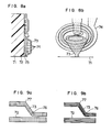
- Figs. 8a and 8b show a magnetic recording thin film head incorporating the laminated magnetic film structure according to the invention, where Fig. 8a illustrates a sectional view of a magnetic head core and Fig. 8b a top view thereof.
- Figs. 8a and 8b there are illustrated a non-magnetic substrate 71, a lower magnetic film structure, an upper magnetic film structure, a conductor coil 74 and a magnetic gap 75.
- the thickness of the magnetic film structure being less than several microns suffices and the non-magnetic insulating film 24 as required for the Fig. 6 example can be dispensed with.
- FIG. 9a and 9b illustrate, in fragmentary enlarged form, a portion of the magnetic film structure near the magnetic gap of the magnetic head shown in Figs. 8a and 8b. More particularly, illustrated in Fig. 9a are magnetic film structures 72 and 73 which are constituted by a single-layer film having a large columnar structure according to the prior art. In this case, the columnar structure is disturbed at bent portions 76 and 77, causing cracks or corrosion thereat. In addition, stress is concentrated at the bent portions to create cracks thereat.
- the crystalline structure is fine and uniformly continuous at the bent portions as shown in Fig. 9b, so that stress concentration at the bent portions can be reduced to suppress the creation of cracks, thereby ensuring provision of a highly corrosion-proof magnetic circuit.
Landscapes
- Engineering & Computer Science (AREA)
- Manufacturing & Machinery (AREA)
- Power Engineering (AREA)
- Thin Magnetic Films (AREA)
- Magnetic Heads (AREA)
Applications Claiming Priority (2)
| Application Number | Priority Date | Filing Date | Title |
|---|---|---|---|
| JP4270/83 | 1983-01-17 | ||
| JP58004270A JPH061729B2 (ja) | 1983-01-17 | 1983-01-17 | 磁性体膜およびそれを用いた磁気ヘッド |
Publications (3)
| Publication Number | Publication Date |
|---|---|
| EP0114076A2 true EP0114076A2 (de) | 1984-07-25 |
| EP0114076A3 EP0114076A3 (en) | 1986-07-23 |
| EP0114076B1 EP0114076B1 (de) | 1992-01-02 |
Family
ID=11579844
Family Applications (1)
| Application Number | Title | Priority Date | Filing Date |
|---|---|---|---|
| EP84100437A Expired - Lifetime EP0114076B1 (de) | 1983-01-17 | 1984-01-17 | Magnetkopf |
Country Status (4)
| Country | Link |
|---|---|
| US (1) | US4610935A (de) |
| EP (1) | EP0114076B1 (de) |
| JP (1) | JPH061729B2 (de) |
| DE (1) | DE3485393D1 (de) |
Cited By (19)
| Publication number | Priority date | Publication date | Assignee | Title |
|---|---|---|---|---|
| EP0185406A1 (de) * | 1984-11-27 | 1986-06-25 | Koninklijke Philips Electronics N.V. | Magnetkopf mit Kernteilen aus ferromagnetischem amorphem Metall |
| EP0147126A3 (en) * | 1983-12-16 | 1986-07-23 | Hitachi, Ltd. | Multilayered ferromagnetic amorphous alloy film and magnetic head employing the same |
| EP0206658A3 (de) * | 1985-06-14 | 1988-10-19 | Hitachi, Ltd. | Magnetkopf |
| US4920013A (en) * | 1986-09-24 | 1990-04-24 | Hitachi, Ltd. | Magnetic Multilayer structure |
| EP0370566A1 (de) * | 1988-11-22 | 1990-05-30 | Koninklijke Philips Electronics N.V. | Weichmagnetischer Mehrschichtfilm und mit einem derartigen weichmagnetischen Mehrschichtfilm versehener Magnetkopf |
| FR2640070A1 (fr) * | 1988-12-06 | 1990-06-08 | Thomson Csf | Tete magnetique planaire d'enregistrement ´ lecture et procede de realisation |
| EP0401983A1 (de) * | 1989-06-02 | 1990-12-12 | Quantum Corporation | Dünnfilm-Vorrichtung zur Rotationsleitung von magnetischem Fluss |
| EP0463753A1 (de) * | 1990-06-29 | 1992-01-02 | Quantum Corporation | Dünnfilmaufzeichnungskopf mit Magnetpolkonfiguration zur Aufzeichnung mit hoher Dichte |
| US5089334A (en) * | 1988-08-03 | 1992-02-18 | Digital Equipment Corporation | Flux spreading thin film magnetic devices |
| US5176965A (en) * | 1987-10-05 | 1993-01-05 | Digital Equipment Corporation | Magnetic medium for longitudinal recording |
| US5184267A (en) * | 1989-06-02 | 1993-02-02 | Digital Equipment Corporation | Transducer with improved inductive coupling |
| US5195005A (en) * | 1989-06-02 | 1993-03-16 | Digital Equipment Corporation | Tranducer with improved inductive coupling |
| EP0426326A3 (en) * | 1989-10-20 | 1993-09-29 | Seagate Technology International | Magnetic read/write head and method of making such a head |
| US5311386A (en) * | 1989-06-02 | 1994-05-10 | Digital Equipment Corporation | Transducer with improved inductive coupling |
| WO1995014991A1 (en) * | 1993-11-23 | 1995-06-01 | Seagate Technology, Inc. | Thin film magnetic heads with thin nickel underlayers |
| US5428893A (en) * | 1989-06-02 | 1995-07-04 | Quantum Corporation | Method of making a transducer with improved inductive coupling |
| US5666250A (en) * | 1993-11-23 | 1997-09-09 | Seagate Technology, Inc. | Thin film magnetic heads with thin nickel underlayers |
| US6125010A (en) * | 1993-11-23 | 2000-09-26 | Seagate Technology Llc | Mo-Au gold seedlayer in thin film heads |
| EP1585149A4 (de) * | 2002-12-26 | 2006-11-22 | Tdk Corp | Dünner magnetfilm oder zusammengesetzter dünner magnetfilm für hochfrequenz und magnetvorrichtung damit |
Families Citing this family (34)
| Publication number | Priority date | Publication date | Assignee | Title |
|---|---|---|---|---|
| JPS6055601A (ja) * | 1983-09-07 | 1985-03-30 | Seiko Epson Corp | 軟磁性薄膜 |
| JPS6159616A (ja) * | 1984-08-29 | 1986-03-27 | Sharp Corp | 磁気ヘツドコアの製造方法 |
| JPS6285413A (ja) * | 1985-10-11 | 1987-04-18 | Hitachi Ltd | 強磁性多層膜及びその製造法 |
| US4897318A (en) * | 1986-01-21 | 1990-01-30 | Matsushita Electric Industrial Co., Ltd. | Laminated magnetic materials |
| US4891278A (en) * | 1986-02-21 | 1990-01-02 | Hitachi, Ltd. | Ferrromagnetic thin film and magnetic head using it |
| US4749628A (en) * | 1986-04-29 | 1988-06-07 | International Business Machines Corporation | Multilayered vertical magnetic recording medium |
| JP2522246B2 (ja) * | 1986-05-06 | 1996-08-07 | ブラザー工業株式会社 | 薄膜磁気記録媒体の製造方法 |
| JPS6365604A (ja) * | 1986-09-05 | 1988-03-24 | Hitachi Ltd | 鉄系磁性体膜 |
| JPH07111925B2 (ja) * | 1986-07-07 | 1995-11-29 | 株式会社日立製作所 | 積層磁性体膜 |
| US4847161A (en) * | 1986-12-19 | 1989-07-11 | Siemens Aktiengesellschaft | Magnetically anisotropic recording medium |
| US4825325A (en) * | 1987-10-30 | 1989-04-25 | International Business Machines Corporation | Magnetoresistive read transducer assembly |
| US5068147A (en) * | 1988-04-28 | 1991-11-26 | Matsushita Electric Industrial Co., Ltd. | Soft magnetic thin film comprising alternate layers of iron carbide with either iron, iron nitride or iron carbon-nitride |
| US5051288A (en) * | 1989-03-16 | 1991-09-24 | International Business Machines Corporation | Thin film magnetic recording disk comprising alternating layers of a CoNi or CoPt alloy and a non-magnetic spacer layer |
| US5576099A (en) * | 1990-02-09 | 1996-11-19 | International Business Machines Corporation | Inductive head lamination with layer of magnetic quenching material |
| US5132859A (en) * | 1990-08-23 | 1992-07-21 | International Business Machines Corporation | Thin film structures for magnetic recording heads |
| US5264981A (en) * | 1991-08-14 | 1993-11-23 | International Business Machines Corporation | Multilayered ferromagnetic film and magnetic head employing the same |
| US5738945A (en) * | 1993-12-16 | 1998-04-14 | Hmt Technology Corporation | Multilayer magnetic medium with soft magnetic interlayer |
| US5660930A (en) * | 1994-04-04 | 1997-08-26 | The Board Of Trustees Of The Leland Stanford Junior University | Multilayered thin films for perpendicular magnetic recording |
| US6259583B1 (en) | 1998-09-16 | 2001-07-10 | International Business Machines, Corporation | Laminated yoke head with a domain control element |
| EP1051635A1 (de) * | 1998-10-30 | 2000-11-15 | Koninklijke Philips Electronics N.V. | Magnetoresistiver magnetfeldsensor |
| US6477765B1 (en) | 1999-11-04 | 2002-11-12 | Storage Technology Corporation | Method of fabricating a magnetic write transducer |
| JP2004235355A (ja) * | 2003-01-29 | 2004-08-19 | Tdk Corp | 軟磁性部材およびそれを用いた磁気素子 |
| US7289297B1 (en) * | 2004-06-07 | 2007-10-30 | Storage Technology Corporation | Multilayered ferromagnetic laminate having alternating cobalt alloy and iron-nitrogen alloy films for use with magnetic heads |
| US7369360B2 (en) * | 2004-11-05 | 2008-05-06 | Seagate Technology Llc | Perpendicular recording head having controlled permeability and saturation moment |
| US20070047140A1 (en) * | 2005-08-29 | 2007-03-01 | Tabakovic Ibro M | Electroplated multiple layer soft magnetic materials with high magnetic moment |
| US8329320B2 (en) * | 2008-11-13 | 2012-12-11 | Headway Technologies, Inc. | Laminated high moment film for head applications |
| US8958176B2 (en) | 2010-12-22 | 2015-02-17 | HGST Netherlands B.V | Write head pole laminate structure |
| US9406319B1 (en) | 2015-06-27 | 2016-08-02 | International Business Machines Corporation | Electrically non-conductive magnetic shield laminate structure for contact recording sensor |
| US9384764B1 (en) | 2015-06-27 | 2016-07-05 | International Business Machines Corporation | Electrically conductive magnetic shield laminate structure for contact recording sensor |
| US9997180B1 (en) | 2017-03-22 | 2018-06-12 | International Business Machines Corporation | Hybrid dielectric gap liner and magnetic shield liner |
| US10803889B2 (en) | 2019-02-21 | 2020-10-13 | International Business Machines Corporation | Apparatus with data reader sensors more recessed than servo reader sensor |
| US11074930B1 (en) | 2020-05-11 | 2021-07-27 | International Business Machines Corporation | Read transducer structure having an embedded wear layer between thin and thick shield portions |
| US11114117B1 (en) | 2020-05-20 | 2021-09-07 | International Business Machines Corporation | Process for manufacturing magnetic head having a servo read transducer structure with dielectric gap liner and a data read transducer structure with an embedded wear layer between thin and thick shield portions |
| CN120581362B (zh) * | 2025-08-01 | 2025-10-24 | 北京航空航天大学 | 一种高熵软磁氮化薄膜磁芯的薄膜电感器制备方法 |
Family Cites Families (15)
| Publication number | Priority date | Publication date | Assignee | Title |
|---|---|---|---|---|
| US3673353A (en) * | 1970-07-16 | 1972-06-27 | Gen Electric | Magnetic transducer having a composite magnetic core structure |
| US3829372A (en) * | 1972-05-25 | 1974-08-13 | Ibm | Multilayer magnetic structure and methods of making same |
| JPS5219680B2 (de) * | 1972-10-23 | 1977-05-30 | ||
| JPS5325410A (en) * | 1976-08-20 | 1978-03-09 | Sony Corp | Magnetic head |
| US4103315A (en) * | 1977-06-24 | 1978-07-25 | International Business Machines Corporation | Antiferromagnetic-ferromagnetic exchange bias films |
| US4156882A (en) * | 1977-12-15 | 1979-05-29 | Texas Instruments Incorporated | Magnetic transducer |
| JPS5530841A (en) * | 1978-08-28 | 1980-03-04 | Toshiba Corp | Clad magnetic material |
| JPS5658125A (en) * | 1979-10-16 | 1981-05-21 | Noboru Tsuya | Magnetic head core |
| JPS5764319A (en) * | 1980-10-02 | 1982-04-19 | Toshiba Corp | Magnetic head and its manufacture |
| JPS57100619A (en) * | 1980-12-12 | 1982-06-22 | Nec Corp | Magnetic head of magnetic tape device |
| JPS57117123A (en) * | 1981-01-13 | 1982-07-21 | Toshiba Corp | Magnetic recoding body |
| US4364020A (en) * | 1981-02-06 | 1982-12-14 | Westinghouse Electric Corp. | Amorphous metal core laminations |
| JPS58128018A (ja) * | 1982-01-22 | 1983-07-30 | Canon Electronics Inc | 磁気ヘツド |
| JPS5933629A (ja) * | 1982-08-17 | 1984-02-23 | Matsushita Electric Ind Co Ltd | 垂直磁気記録媒体の製造方法 |
| JPH0622170B2 (ja) * | 1983-12-16 | 1994-03-23 | 株式会社日立製作所 | 磁気ヘッド |
-
1983
- 1983-01-17 JP JP58004270A patent/JPH061729B2/ja not_active Expired - Lifetime
-
1984
- 1984-01-16 US US06/571,099 patent/US4610935A/en not_active Expired - Lifetime
- 1984-01-17 DE DE8484100437T patent/DE3485393D1/de not_active Expired - Lifetime
- 1984-01-17 EP EP84100437A patent/EP0114076B1/de not_active Expired - Lifetime
Cited By (24)
| Publication number | Priority date | Publication date | Assignee | Title |
|---|---|---|---|---|
| EP0147126A3 (en) * | 1983-12-16 | 1986-07-23 | Hitachi, Ltd. | Multilayered ferromagnetic amorphous alloy film and magnetic head employing the same |
| US4748089A (en) * | 1983-12-16 | 1988-05-31 | Hitachi, Ltd. | Multilayered ferromagnetic amorphous alloy film and magnetic head employing the same |
| EP0185406A1 (de) * | 1984-11-27 | 1986-06-25 | Koninklijke Philips Electronics N.V. | Magnetkopf mit Kernteilen aus ferromagnetischem amorphem Metall |
| EP0206658A3 (de) * | 1985-06-14 | 1988-10-19 | Hitachi, Ltd. | Magnetkopf |
| US4920013A (en) * | 1986-09-24 | 1990-04-24 | Hitachi, Ltd. | Magnetic Multilayer structure |
| US5431969A (en) * | 1987-10-05 | 1995-07-11 | Quantum Corporation | Method of making a magnetic medium for longitudinal recording |
| US5176965A (en) * | 1987-10-05 | 1993-01-05 | Digital Equipment Corporation | Magnetic medium for longitudinal recording |
| US5089334A (en) * | 1988-08-03 | 1992-02-18 | Digital Equipment Corporation | Flux spreading thin film magnetic devices |
| US5085935A (en) * | 1988-08-03 | 1992-02-04 | Digital Equipment Corporation | Flux spreading thin film magnetic devices |
| EP0370566A1 (de) * | 1988-11-22 | 1990-05-30 | Koninklijke Philips Electronics N.V. | Weichmagnetischer Mehrschichtfilm und mit einem derartigen weichmagnetischen Mehrschichtfilm versehener Magnetkopf |
| FR2640070A1 (fr) * | 1988-12-06 | 1990-06-08 | Thomson Csf | Tete magnetique planaire d'enregistrement ´ lecture et procede de realisation |
| EP0401983A1 (de) * | 1989-06-02 | 1990-12-12 | Quantum Corporation | Dünnfilm-Vorrichtung zur Rotationsleitung von magnetischem Fluss |
| US5184267A (en) * | 1989-06-02 | 1993-02-02 | Digital Equipment Corporation | Transducer with improved inductive coupling |
| US5195005A (en) * | 1989-06-02 | 1993-03-16 | Digital Equipment Corporation | Tranducer with improved inductive coupling |
| US5311386A (en) * | 1989-06-02 | 1994-05-10 | Digital Equipment Corporation | Transducer with improved inductive coupling |
| US5428887A (en) * | 1989-06-02 | 1995-07-04 | Quantum Corporation | Method of making a transducer with improved inductive coupling |
| US5428893A (en) * | 1989-06-02 | 1995-07-04 | Quantum Corporation | Method of making a transducer with improved inductive coupling |
| EP0426326A3 (en) * | 1989-10-20 | 1993-09-29 | Seagate Technology International | Magnetic read/write head and method of making such a head |
| EP0463753A1 (de) * | 1990-06-29 | 1992-01-02 | Quantum Corporation | Dünnfilmaufzeichnungskopf mit Magnetpolkonfiguration zur Aufzeichnung mit hoher Dichte |
| US5157570A (en) * | 1990-06-29 | 1992-10-20 | Digital Equipment Corporation | Magnetic pole configuration for high density thin film recording head |
| WO1995014991A1 (en) * | 1993-11-23 | 1995-06-01 | Seagate Technology, Inc. | Thin film magnetic heads with thin nickel underlayers |
| US5666250A (en) * | 1993-11-23 | 1997-09-09 | Seagate Technology, Inc. | Thin film magnetic heads with thin nickel underlayers |
| US6125010A (en) * | 1993-11-23 | 2000-09-26 | Seagate Technology Llc | Mo-Au gold seedlayer in thin film heads |
| EP1585149A4 (de) * | 2002-12-26 | 2006-11-22 | Tdk Corp | Dünner magnetfilm oder zusammengesetzter dünner magnetfilm für hochfrequenz und magnetvorrichtung damit |
Also Published As
| Publication number | Publication date |
|---|---|
| JPH061729B2 (ja) | 1994-01-05 |
| JPS59130408A (ja) | 1984-07-27 |
| EP0114076A3 (en) | 1986-07-23 |
| DE3485393D1 (de) | 1992-02-13 |
| EP0114076B1 (de) | 1992-01-02 |
| US4610935A (en) | 1986-09-09 |
Similar Documents
| Publication | Publication Date | Title |
|---|---|---|
| EP0114076B1 (de) | Magnetkopf | |
| EP0144150B2 (de) | Ferromagnetischer Werkstoff, ferromagnetisches Laminat und Magnetkopf | |
| US4049522A (en) | Low coercivity iron-silicon material, shields, and process | |
| US5302469A (en) | Soft magnetic thin film | |
| JPH0834154B2 (ja) | 軟磁性薄膜 | |
| EP0247868B1 (de) | Magnetischer Film und denselben verwendender Magnetkopf | |
| EP0159028B1 (de) | Magnetischer dünner Film | |
| EP0234879B1 (de) | Ferromagnetischer dünner Film und ihn verwendender Magnetkopf | |
| JPS599905A (ja) | 磁性体膜およびそれを用いた磁気ヘッド | |
| EP0122792B1 (de) | Amorphe magnetische Legierung des Co-Nb-Zr Systems und Magnetkopf aus dieser Legierung | |
| US4752344A (en) | Magnetic layer and method of manufacture | |
| EP0178634B1 (de) | Amorpher weichmagnetischer dünner Film | |
| EP0438687A1 (de) | Mehrlagiger Film aus Eisen und Eisennitrid | |
| US5411813A (en) | Ferhgasi soft magnetic materials for inductive magnetic heads | |
| JPH0462162B2 (de) | ||
| Snyder et al. | Influence of deposition conditions on magnetic properties of CoCr thin films | |
| JP3232592B2 (ja) | 磁気ヘッド | |
| JPH03265105A (ja) | 軟磁性積層膜 | |
| Hoshi et al. | Magnetic properties of zero magnetostriction Co-Ta-Zr amorphous alloy films deposited by RF sputtering | |
| JPS58100412A (ja) | 軟質磁性材料の製法 | |
| JP2638739B2 (ja) | 磁性薄膜及びその製造方法 | |
| JP3036891B2 (ja) | 薄膜磁気ヘッド | |
| JPS5877017A (ja) | 薄膜磁気ヘツド | |
| JP2546275B2 (ja) | 軟磁性薄膜 | |
| JPS61233409A (ja) | 高周波用積層型磁気ヘツドコアの製造方法及び磁気ヘツドコア |
Legal Events
| Date | Code | Title | Description |
|---|---|---|---|
| PUAI | Public reference made under article 153(3) epc to a published international application that has entered the european phase |
Free format text: ORIGINAL CODE: 0009012 |
|
| 17P | Request for examination filed |
Effective date: 19840117 |
|
| AK | Designated contracting states |
Designated state(s): DE FR GB NL |
|
| PUAL | Search report despatched |
Free format text: ORIGINAL CODE: 0009013 |
|
| AK | Designated contracting states |
Kind code of ref document: A3 Designated state(s): DE FR GB NL |
|
| 17Q | First examination report despatched |
Effective date: 19900214 |
|
| GRAA | (expected) grant |
Free format text: ORIGINAL CODE: 0009210 |
|
| AK | Designated contracting states |
Kind code of ref document: B1 Designated state(s): DE FR GB NL |
|
| PG25 | Lapsed in a contracting state [announced via postgrant information from national office to epo] |
Ref country code: NL Effective date: 19920102 |
|
| REF | Corresponds to: |
Ref document number: 3485393 Country of ref document: DE Date of ref document: 19920213 |
|
| PG25 | Lapsed in a contracting state [announced via postgrant information from national office to epo] |
Ref country code: GB Effective date: 19920402 |
|
| EN | Fr: translation not filed | ||
| PG25 | Lapsed in a contracting state [announced via postgrant information from national office to epo] |
Ref country code: FR Effective date: 19920522 |
|
| NLV1 | Nl: lapsed or annulled due to failure to fulfill the requirements of art. 29p and 29m of the patents act | ||
| PLBE | No opposition filed within time limit |
Free format text: ORIGINAL CODE: 0009261 |
|
| STAA | Information on the status of an ep patent application or granted ep patent |
Free format text: STATUS: NO OPPOSITION FILED WITHIN TIME LIMIT |
|
| GBPC | Gb: european patent ceased through non-payment of renewal fee | ||
| 26N | No opposition filed | ||
| PGFP | Annual fee paid to national office [announced via postgrant information from national office to epo] |
Ref country code: LU Payment date: 19930119 Year of fee payment: 10 |
|
| REG | Reference to a national code |
Ref country code: FR Ref legal event code: ST |
|
| EPTA | Lu: last paid annual fee | ||
| PGFP | Annual fee paid to national office [announced via postgrant information from national office to epo] |
Ref country code: DE Payment date: 19980225 Year of fee payment: 15 |
|
| PG25 | Lapsed in a contracting state [announced via postgrant information from national office to epo] |
Ref country code: DE Free format text: LAPSE BECAUSE OF NON-PAYMENT OF DUE FEES Effective date: 19991103 |