EP0114382A2 - Dispositif semi-conducteur du type MOS comportant un transistor à effet de champ et une couche métallique d'interconnexion - Google Patents
Dispositif semi-conducteur du type MOS comportant un transistor à effet de champ et une couche métallique d'interconnexion Download PDFInfo
- Publication number
- EP0114382A2 EP0114382A2 EP83112993A EP83112993A EP0114382A2 EP 0114382 A2 EP0114382 A2 EP 0114382A2 EP 83112993 A EP83112993 A EP 83112993A EP 83112993 A EP83112993 A EP 83112993A EP 0114382 A2 EP0114382 A2 EP 0114382A2
- Authority
- EP
- European Patent Office
- Prior art keywords
- wiring layer
- metal wiring
- layer
- semiconductor device
- end connected
- Prior art date
- Legal status (The legal status is an assumption and is not a legal conclusion. Google has not performed a legal analysis and makes no representation as to the accuracy of the status listed.)
- Granted
Links
Images


Classifications
-
- H—ELECTRICITY
- H10—SEMICONDUCTOR DEVICES; ELECTRIC SOLID-STATE DEVICES NOT OTHERWISE PROVIDED FOR
- H10W—GENERIC PACKAGES, INTERCONNECTIONS, CONNECTORS OR OTHER CONSTRUCTIONAL DETAILS OF DEVICES COVERED BY CLASS H10
- H10W20/00—Interconnections in chips, wafers or substrates
- H10W20/40—Interconnections external to wafers or substrates, e.g. back-end-of-line [BEOL] metallisations or vias connecting to gate electrodes
- H10W20/41—Interconnections external to wafers or substrates, e.g. back-end-of-line [BEOL] metallisations or vias connecting to gate electrodes characterised by their conductive parts
- H10W20/43—Layouts of interconnections
-
- H—ELECTRICITY
- H10—SEMICONDUCTOR DEVICES; ELECTRIC SOLID-STATE DEVICES NOT OTHERWISE PROVIDED FOR
- H10D—INORGANIC ELECTRIC SEMICONDUCTOR DEVICES
- H10D84/00—Integrated devices formed in or on semiconductor substrates that comprise only semiconducting layers, e.g. on Si wafers or on GaAs-on-Si wafers
- H10D84/01—Manufacture or treatment
-
- H—ELECTRICITY
- H10—SEMICONDUCTOR DEVICES; ELECTRIC SOLID-STATE DEVICES NOT OTHERWISE PROVIDED FOR
- H10D—INORGANIC ELECTRIC SEMICONDUCTOR DEVICES
- H10D84/00—Integrated devices formed in or on semiconductor substrates that comprise only semiconducting layers, e.g. on Si wafers or on GaAs-on-Si wafers
- H10D84/01—Manufacture or treatment
- H10D84/0123—Integrating together multiple components covered by H10D12/00 or H10D30/00, e.g. integrating multiple IGBTs
- H10D84/0126—Integrating together multiple components covered by H10D12/00 or H10D30/00, e.g. integrating multiple IGBTs the components including insulated gates, e.g. IGFETs
- H10D84/0165—Integrating together multiple components covered by H10D12/00 or H10D30/00, e.g. integrating multiple IGBTs the components including insulated gates, e.g. IGFETs the components including complementary IGFETs, e.g. CMOS devices
- H10D84/0193—Integrating together multiple components covered by H10D12/00 or H10D30/00, e.g. integrating multiple IGBTs the components including insulated gates, e.g. IGFETs the components including complementary IGFETs, e.g. CMOS devices the components including FinFETs
Definitions
- the present invention relates to a MOS semiconductor device in which a logic circuit is formed below a wide power supply wiring layer.
- an output circuit of an I/O (Input/Output) port of an LSI (Large Scale Integrated Circuit) in a microcomputer or the like a buffer circuit for producing data outside the LSI is arranged.
- a transistor having a relatively high conductance is used for such an output buffer circuit. This is because a large current of 1.6 mA flows to the buffer circuit at a low output voltage VOL of 0.4 V, for example.
- VOL output voltage
- LSI for a microcomputer a number of transistors having a relatively high conductance are used.
- An LSI of an 8-bit microcomputer having two I/O ports requires a total of 24 (8 x 3) output buffers (two I/O ports and one data bus port).
- the power supply line for all the I/O ports is a very wide metal wiring layer.
- a power supply line comprising such a wide metal wiring layer increases the pattern area and is not preferable for an LSI.
- the use of a wide metal wiring layer as a power supply line cannot be avoided in view of the electrical characteristics as described above. For this reason, there is a demand to effectively utilize a region below such a wide power supply line.
- CMOS Complementary Metal Oxide Semiconductor
- F ig. 1 shows a CMOS inverter which is formed below a wide power supply line.
- a first metal wiring layer 11 of aluminum or the like supplies a signal A
- a second metal wiring layer 12 of aluminum or the like supplies a power supply voltage VDD
- a third metal wiring layer 13 of aluminum or the like is at ground potential.
- the third metal wiring layer 13 is formed in a very wide pattern.
- a p-type well region 14 is formed in an n-type semiconductor substrate 10.
- a source region 151 and a drain region 152 in the p-type well region 14 comprise an n +- type diffusion layer.
- a source electrode Sl, a gate electrode Gl, and a drain electrode Dl are formed in the p-type well region 14.
- a source region 161 and a drain region 162 of a p +- type diffusion layer are formed outside the p-type well region 14 on the semiconductor substrate 10.
- a source electrode S2, a gate electrode G2, and a drain electrode D2 are formed outside the p-type well region 14.
- the gate electrodes Gl and G2 are connected to a first polycrystalline silicon layer 17 formed below the first through third metal wiring layers 11 to 13.
- the first polycrystalline silicon layer 17 is connected to the first metal wiring layer 11 through a contact hole Cl.
- the drain electrode Dl is connected to a fourth metal wiring layer 18 of aluminum or the like through contact holes C2 and C3.
- the fourth metal wiring layer 18 is connected to an underlying second polycrystalline silicon layer 19 through a contact hole C4.
- An inverted signal A of the signal A supplied through the first metal wiring layer 11 is obtained from the second polycrystalline silicon layer 19.
- the source electrode Sl is connected to the third metal wiring layer 13 through a contact hole C5.
- the source electrode S2 is connected to the second metal wiring layer 12 through a contact hole C6. In this manner, a CMOS inverter for inverting the input signal A and producing an inverted signal A is obtained.
- the signal A is supplied to the gate electrodes Gl and G2 through the long, first polycrystalline silicon layer 17 below the third metal wiring layer 13. This is for reducing the areas of the drain regions 152 and 162 to decrease the output capacitance for high speed operation of the CMOS inverter.
- the first polycrystalline silicon layer 17 is long, the input resistance of the CMOS inverter is increased. This results in a lower operation speed of the CMOS inverter.
- Fig. 2 shows a CMOS inverter wherein the length of the first polycrystalline silicon layer 17 shown in Fig. 1 is short to reduce the input resistance of the CMOS inverter.
- the same reference numerals as used in Fig. 1 denote the same parts.
- a MOS semiconductor device comprising: a semiconductor substrate; a power supply metal wiring layer formed on said semiconductor substrate; an opening formed at a position substantially midway along a widthwise direction of said metal wiring layer; a contact layer formed in said opening as isolated from said metal wiring layer; a MOS logic circuit including at least one FET having a drain and source formed below said metal wiring layer; means for connecting said drain to said contact layer; and an output wiring layer of said MOS logic circuit, which is connected to said contact layer.
- the input resistance and drain capacitance of the MOS logic circuit formed below a wide power supply line can be reduced, so that a MOS semiconductor device which can operate the MOS logic circuit at high speed can be obtained.
- An opening 21 is formed at substantially the center of a third metal wiring layer 13.
- drain electrodes Dl and D2 are connected to the fourth metal wiring layer 18 through contact holes C2 and C3.
- the fourth metal wiring layer 18 is also connected to a second polycrystalline silicon layer 19 through a contact hole C4.
- An inverted signal A of a signal A supplied through a first polycrystalline silicon layer 17 is obtained through a second polycrystalline silicon layer 19.
- the length of the first polycrystalline silicon layer 17 shown in F ig. 3 is about half of that of the first polycrystalline silicon layer 17 shown in Fig. 1.
- the input resistance of the CMOS inverter shown in Fig. 3 can be reduced.
- the areas of drain regions 152 and 162 of the CMOS inverter shown in Fig. 3 are significantly smaller than those of the CMOS inverter shown in Fig. 2. For this reason, the drain capacitance of the CMOS inverter can be significantly reduced. Since the input resistance and the drain capacitance of the CMOS inverter can be reduced, the CMOS inverter can operate at high speed.
- CMOS inverter in which an input signal is obtained from a metal wiring layer lying below the third metal wiring layer 13 and an output signal is obtained from a metal wiring layer lying above the layer 13 is formed below the metal wiring layer 13, and if the opening 21 is formed at a position substantially midway along the widthwise direction of the layer 13, the input resistance and the drain capacitance can be significantly reduced.
- the second polycrystalline silicon layer 19 of the CMOS inverter shown in Fig. 3 has a length substantially half the width of the third metal wiring layer 13. Then, the resistance of the second polycrystalline silicon layer 19 would apparently interfere with high-speed operation of the CMOS inverter. However, this can be prevented by forming a sufficiently wide second polycrystalline silicon layer.
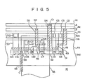
- F ig. 4 is a circuit diagram of the logic circuit realized by the structure shown in Fig. 5.
- signals A and B are supplied to a N AN D circuit 31, which produces an output signal C through an inverter 32.
- the NAND circuit 31 and the inverter 32 comprise CMOSFETs.
- a first metal wiring layer 41 of aluminum or the like supplies a signal A
- a second metal wiring layer 42 of aluminum or the like supplies a signal B
- a third metal wiring layer 43 of aluminum or the like supplies a power supply voltage VDD
- a fourth metal wiring layer 44 of aluminum or the like is at ground potential.
- the fourth metal wiring layer 44 comprises a very wide pattern.
- a p-type well region 45 is formed in an n-type semiconductor substrate 10.
- N-channel MOSFETs 46 and 47 are formed in the p-type well region 45.
- P-channel MOSFETs 48 to 50 are formed outside the p-type well region 45 of the semiconductor substrate 10.
- the n-channel MOSFET 46 and the p-channel MOSFETs 48 and 49 constitute a NAND circuit 31, and the n-channel MOSFET 47 and the p-channel MOSFET 50 constitute an inverter 32.
- An opening 51 is formed at a position substantially midway along a widthwise direction of the fourth metal wiring layer 44.
- Fifth and sixth metal wiring layers 52 and 53 of aluminum or the like are formed in the opening 51 as contact layers formed in the same step as that for forming the fourth metal wiring layer 44.
- the first metal wiring layer 41 is connected to one end of a first polycrystalline silicon layer 54 through a contact hole Cl.
- the other end of the first polycrystalline silicon layer 54 is connected to the gates of the n- and p-channel MOSFETs 46 and 49.
- the second metal wiring layer 42 is connected to one end of a second polycrystalline silicon layer 55 through a contact hole C2.
- the other end of the second polycrystalline silicon layer 55 is connected to the gate of the n-channel MOSFET 46.
- the second metal wiring layer 42 is also connected to one end of a third polycrystalline silicon layer 56 through a contact hole C3.
- the other end of the third polycrystalline silicon layer 56 is connected to the gate of the p-channel MOSFET 48.
- the source electrode of the n-channel MOSFET 46 is connected to the fourth metal wiring layer 44 through a contact hole C4, and the source electrodes of the p-channel MOSFETs 48 and 49 are connected to the third metal wiring layer 43 through contact holes C5 and C6, respectively.
- the drain electrodes of the n-channel MOSFET 46 and the p-channel MOSFETs 48 and 49 are connected to the fifth metal wiring layer 52 through contact holes C7 to C9, respectively.
- the fifth metal wiring layer 52 is connected to one end of a fourth polycrystalline silicon layer 57 through a contact hole C10.
- the other end of the polycrystalline silicon layer 57 is connected to the gate electrodes of the n- and p-channel MOSFETs 47 and 50.
- the source electrode of the n-channel MOSFET 47 is connected to the fourth metal wiring layer 44 through a contact hole Cll
- the source electrode of the p-channel MOSFET 50 is connected to the third metal wiring layer 43 through a contact hole C12.
- the drain electrodes of the n- and p-channel MOSFETs 47 and 50 are connected to the sixth metal wiring layer 53 through contact holes C13 and C14, respectively.
- the sixth metal wiring layer 53 is connected to a fifth polycrystalline silicon layer 58 through a contact hole C15.
- a signal C is obtained from the fifth polycrystalline silicon layer 58.
- the lengths of the first through third polycrystalline silicon layers 54 to 56 are substantially half the length of the polycrystalline silicon layer 17 shown in Fig. 1. Therefore, the input resistance of the logic circuit shown in Fig. 5 can be reduced. Moreover, the drain regions of the n-channel MOSFETs 46 and 47 and those of the p-channel MOSFETs 48 to 50 are significantly smaller than those of the CMOS inverter shown in Fig. 2. Thus, the drain capacitance of the logic circuit shown in Fig. 5 can be significantly reduced. Since the input resistance and drain capacitance of the logic circuit shown in Fig. 5 can be reduced, the logic circuit can operate at high speed. Since the width of the fifth polycrystalline silicon layer 58 is sufficiently great, high-speed operation of the CMOS inverter is not interfered with as in the case of the former embodiment of the present invention.
- the input resistance and the drain capacitance can be significantly reduced when a logic circuit consisting of a series circuit of a CMOS NAND gate and a CMOS inverter is formed below the fourth metal wiring layer 44 and if an opening 51 is formed at a position substantially midway along the widthwise direction of the fourth metal wiring layer 44, an input signal being obtained from the metal wiring layer lying below the fourth metal wiring layer 44 and an output signal being supplied to the metal wiring layer lying above the fourth metal wiring layer 44 in the CMOS NAND gate.
- the opening 21 or 51 is formed at a position substantially midway along the widthwise direction of the third or fourth metal wiring layer 13 or 44, respectively.
- the position of the opening is not limited to this.
Landscapes
- Metal-Oxide And Bipolar Metal-Oxide Semiconductor Integrated Circuits (AREA)
- Design And Manufacture Of Integrated Circuits (AREA)
- Internal Circuitry In Semiconductor Integrated Circuit Devices (AREA)
Applications Claiming Priority (2)
| Application Number | Priority Date | Filing Date | Title |
|---|---|---|---|
| JP234015/82 | 1982-12-27 | ||
| JP57234015A JPS59121853A (ja) | 1982-12-27 | 1982-12-27 | 半導体装置 |
Publications (3)
| Publication Number | Publication Date |
|---|---|
| EP0114382A2 true EP0114382A2 (fr) | 1984-08-01 |
| EP0114382A3 EP0114382A3 (en) | 1985-07-31 |
| EP0114382B1 EP0114382B1 (fr) | 1987-08-19 |
Family
ID=16964214
Family Applications (1)
| Application Number | Title | Priority Date | Filing Date |
|---|---|---|---|
| EP83112993A Expired EP0114382B1 (fr) | 1982-12-27 | 1983-12-22 | Dispositif semi-conducteur du type MOS comportant un transistor à effet de champ et une couche métallique d'interconnexion |
Country Status (4)
| Country | Link |
|---|---|
| US (1) | US4740825A (fr) |
| EP (1) | EP0114382B1 (fr) |
| JP (1) | JPS59121853A (fr) |
| DE (1) | DE3373164D1 (fr) |
Families Citing this family (5)
| Publication number | Priority date | Publication date | Assignee | Title |
|---|---|---|---|---|
| JPH06101532B2 (ja) * | 1986-10-29 | 1994-12-12 | 三菱電機株式会社 | 半導体集積回路装置 |
| EP0550177B1 (fr) * | 1991-12-30 | 2002-04-10 | AT&T Corp. | Circuit intégré de mémoire RAM statique avec résistance équilibrée |
| US5416431A (en) * | 1994-03-21 | 1995-05-16 | At&T Corp. | Integrated circuit clock driver having improved layout |
| US5804477A (en) * | 1997-02-24 | 1998-09-08 | Integrated Device Technology, Inc. | Method of making a 6-transistor compact static ram cell |
| KR100884450B1 (ko) * | 2007-11-08 | 2009-02-19 | 삼성모바일디스플레이주식회사 | 유기전계발광 표시장치 |
Family Cites Families (7)
| Publication number | Priority date | Publication date | Assignee | Title |
|---|---|---|---|---|
| JPS5620734B2 (fr) * | 1973-07-31 | 1981-05-15 | ||
| US4152717A (en) * | 1975-07-18 | 1979-05-01 | Tokyo Shibaura Electric Co., Ltd. | Complementary MOSFET device |
| JPS5598852A (en) * | 1979-01-23 | 1980-07-28 | Nec Corp | Memory device |
| US4453175A (en) * | 1979-09-19 | 1984-06-05 | Tokyo Shibaura Denki Kabushiki Kaisha | MOS Static RAM layout with polysilicon resistors over FET gates |
| JPS5644194A (en) * | 1979-09-19 | 1981-04-23 | Toshiba Corp | Memory device |
| JPS58216440A (ja) * | 1982-06-10 | 1983-12-16 | Nec Corp | 半導体装置 |
| JPS5914647A (ja) * | 1982-07-16 | 1984-01-25 | Nec Corp | マスタ−スライス半導体装置 |
-
1982
- 1982-12-27 JP JP57234015A patent/JPS59121853A/ja active Pending
-
1983
- 1983-12-22 EP EP83112993A patent/EP0114382B1/fr not_active Expired
- 1983-12-22 DE DE8383112993T patent/DE3373164D1/de not_active Expired
-
1987
- 1987-01-30 US US07/009,553 patent/US4740825A/en not_active Expired - Lifetime
Also Published As
| Publication number | Publication date |
|---|---|
| JPS59121853A (ja) | 1984-07-14 |
| DE3373164D1 (en) | 1987-09-24 |
| EP0114382B1 (fr) | 1987-08-19 |
| US4740825A (en) | 1988-04-26 |
| EP0114382A3 (en) | 1985-07-31 |
Similar Documents
| Publication | Publication Date | Title |
|---|---|---|
| US4733288A (en) | Gate-array chip | |
| EP0080361B1 (fr) | Dispositif de circuits intégrés du type à tranche maîtresse comprenant des semi-conducteurs métal-oxyde complémentaires | |
| US4635088A (en) | High speed-low power consuming IGFET integrated circuit | |
| US4771327A (en) | Master-slice integrated circuit having an improved arrangement of transistor elements for simplified wirings | |
| US5302871A (en) | Delay circuit | |
| US4356504A (en) | MOS Integrated circuit structure for discretionary interconnection | |
| KR100223352B1 (ko) | 반도체 집적 회로 장치 | |
| KR100302529B1 (ko) | 박막반도체집적회로 | |
| US5083178A (en) | Semiconductor cmos gate array | |
| US5404035A (en) | Multi-voltage-level master-slice integrated circuit | |
| US5539246A (en) | Microelectronic integrated circuit including hexagonal semiconductor "gate " device | |
| EP0114382B1 (fr) | Dispositif semi-conducteur du type MOS comportant un transistor à effet de champ et une couche métallique d'interconnexion | |
| US5416431A (en) | Integrated circuit clock driver having improved layout | |
| US4951111A (en) | Integrated circuit device | |
| US5355004A (en) | Semiconductor integrated circuit device having wiring for clock signal supply | |
| KR940004455B1 (ko) | Cmos 반도체 집적 회로 장치 | |
| EP0092176A2 (fr) | Cellule de base pour réseau de portes à circuit intégré | |
| JPS60154553A (ja) | 相補型mos集積回路の駆動方法 | |
| EP0344055B1 (fr) | Dispositif de circuit intégré semi-conducteur | |
| US5498897A (en) | Transistor layout for semiconductor integrated circuit | |
| JP3119177B2 (ja) | 半導体装置 | |
| US20020125912A1 (en) | Tri-state buffer circuit | |
| US5656850A (en) | Microelectronic integrated circuit including hexagonal semiconductor "and"g | |
| US4318117A (en) | MOS Integrated circuit | |
| EP0467361B1 (fr) | Dispositif à matrice de portes en technologie BICMOS |
Legal Events
| Date | Code | Title | Description |
|---|---|---|---|
| PUAI | Public reference made under article 153(3) epc to a published international application that has entered the european phase |
Free format text: ORIGINAL CODE: 0009012 |
|
| 17P | Request for examination filed |
Effective date: 19831222 |
|
| AK | Designated contracting states |
Designated state(s): DE GB IT |
|
| RAP1 | Party data changed (applicant data changed or rights of an application transferred) |
Owner name: KABUSHIKI KAISHA TOSHIBA |
|
| PUAL | Search report despatched |
Free format text: ORIGINAL CODE: 0009013 |
|
| AK | Designated contracting states |
Designated state(s): DE GB IT |
|
| 17Q | First examination report despatched |
Effective date: 19861024 |
|
| GRAA | (expected) grant |
Free format text: ORIGINAL CODE: 0009210 |
|
| AK | Designated contracting states |
Kind code of ref document: B1 Designated state(s): DE GB IT |
|
| ITF | It: translation for a ep patent filed | ||
| REF | Corresponds to: |
Ref document number: 3373164 Country of ref document: DE Date of ref document: 19870924 |
|
| PLBI | Opposition filed |
Free format text: ORIGINAL CODE: 0009260 |
|
| 26 | Opposition filed |
Opponent name: DEUTSCHE ITT INDUSTRIES GMBH, FREIBURG Effective date: 19880513 |
|
| PLAB | Opposition data, opponent's data or that of the opponent's representative modified |
Free format text: ORIGINAL CODE: 0009299OPPO |
|
| R26 | Opposition filed (corrected) |
Opponent name: DEUTSCHE ITT INDUSTRIES GMBH, FREIBURG Effective date: 19880818 |
|
| PLBN | Opposition rejected |
Free format text: ORIGINAL CODE: 0009273 |
|
| STAA | Information on the status of an ep patent application or granted ep patent |
Free format text: STATUS: OPPOSITION REJECTED |
|
| 27O | Opposition rejected |
Effective date: 19900327 |
|
| ITTA | It: last paid annual fee | ||
| REG | Reference to a national code |
Ref country code: GB Ref legal event code: 746 Effective date: 19981105 |
|
| PGFP | Annual fee paid to national office [announced via postgrant information from national office to epo] |
Ref country code: GB Payment date: 19991222 Year of fee payment: 17 |
|
| PGFP | Annual fee paid to national office [announced via postgrant information from national office to epo] |
Ref country code: DE Payment date: 19991230 Year of fee payment: 17 |
|
| PG25 | Lapsed in a contracting state [announced via postgrant information from national office to epo] |
Ref country code: GB Free format text: LAPSE BECAUSE OF NON-PAYMENT OF DUE FEES Effective date: 20001222 |
|
| GBPC | Gb: european patent ceased through non-payment of renewal fee |
Effective date: 20001222 |
|
| PG25 | Lapsed in a contracting state [announced via postgrant information from national office to epo] |
Ref country code: DE Free format text: LAPSE BECAUSE OF NON-PAYMENT OF DUE FEES Effective date: 20011002 |