EP0114652A2 - Target für Bildaufnahmeröhre - Google Patents
Target für Bildaufnahmeröhre Download PDFInfo
- Publication number
- EP0114652A2 EP0114652A2 EP84100470A EP84100470A EP0114652A2 EP 0114652 A2 EP0114652 A2 EP 0114652A2 EP 84100470 A EP84100470 A EP 84100470A EP 84100470 A EP84100470 A EP 84100470A EP 0114652 A2 EP0114652 A2 EP 0114652A2
- Authority
- EP
- European Patent Office
- Prior art keywords
- layer
- image pickup
- pickup tube
- tube target
- target according
- Prior art date
- Legal status (The legal status is an assumption and is not a legal conclusion. Google has not performed a legal analysis and makes no representation as to the accuracy of the status listed.)
- Granted
Links
Images

Classifications
-
- H—ELECTRICITY
- H01—ELECTRIC ELEMENTS
- H01J—ELECTRIC DISCHARGE TUBES OR DISCHARGE LAMPS
- H01J29/00—Details of cathode-ray tubes or of electron-beam tubes of the types covered by group H01J31/00
- H01J29/02—Electrodes; Screens; Mounting, supporting, spacing or insulating thereof
- H01J29/10—Screens on or from which an image or pattern is formed, picked up, converted or stored
- H01J29/36—Photoelectric screens; Charge-storage screens
- H01J29/39—Charge-storage screens
- H01J29/45—Charge-storage screens exhibiting internal electric effects caused by electromagnetic radiation, e.g. photoconductive screen, photodielectric screen, photovoltaic screen
- H01J29/451—Charge-storage screens exhibiting internal electric effects caused by electromagnetic radiation, e.g. photoconductive screen, photodielectric screen, photovoltaic screen with photosensitive junctions
- H01J29/456—Charge-storage screens exhibiting internal electric effects caused by electromagnetic radiation, e.g. photoconductive screen, photodielectric screen, photovoltaic screen with photosensitive junctions exhibiting no discontinuities, e.g. consisting of uniform layers
Definitions
- the present invention relates to an image pickup tube target and, more particularly, to a structure of a Se-As-Te type chalcogen photoconductive film (Saticon film) with improved sticking characteristics.
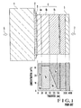
- Fig. 1 shows a section of a main part of a conventional image pickup tube target and a concentration distribution of selenium, arsenic and tellurium as major constituents of a photoconductive film.
- a transparent conductive film 2 containing Sn0 2 or In 2 0 3 as a major constitutent is formed on the rear major surface of a disc-like translucent glass substrate 1.
- a very thin N-type transparent Ce0 2 conductive film 3 serving as a blocking layer is formed on the rear major surface of the transparent conductive film 2.
- a P-type photoconductive film 4 comprising a P-type Se-As-Te amorphous semiconductor film is formed on the rear major surface of the N-type transparent conductive film 3.
- a P-type Sb 2 S 3 photoconductive film 5 serving as a beam landing layer is formed on the rear major surface of the P-type photoconductive film 4.
- the P-type photoconductive film 4 consists of first, second and third P-type photoconductive layers 4a, 4b and 4c.
- the first P-type photoconductive layer 4a comprises a P-type Se-As amorphous semiconductor film having an Se concentration of 97 to 88 wt% and an As concentration of 3 to 12 wt% and is formed on the rear major surface of the N-type transparent conductive film 3 to have a thickness of 30 to 60 nm.
- the second P-type photoconductive layer 4b comprises a P-type Se-As-Te amorphous semiconductor film having an Se concentration of about 67 wt%, an As concentration of 3 wt%, and a Te concentration of about 30 wt% and is formed on the rear major surface of the first P-type photoconductive layer 4a to have a thickness of about 60 nm.
- the third P-type photoconductive layer 4c is formed on the rear major surface of the second P-type photoconductive layer 4b such that a total thickness of the multilayer film 4 is set to be about 3900 nm, for example.
- the third P-type photoconductive layer 4c comprises a P-type Se-As amorphous semiconductor film wherein in the Se-As concentration distribution, the As concentration continuously changes from 20 to 30 wt% to 3 2 wt% over a thickness of 45 ⁇ 20 nm which starts from the interface between the second and third P-type photoconductive layers 4b and 4c.
- the 3 t 2 wt% As concentration remains unchanged as the thickness increases.
- the P-type photocoductive film 5 is formed on the rear major surface of the multilayer film 4.
- a light beam 6 is incident on the front major surface of the glass substrate 1, and a scanning electron beam 7 is supplied to the P-type photoconductive film 5.
- the gradient As concentration layer as part of the third P-type photoconductive layer 4c serves as a carrier extraction layer for effectively and stably extracting carriers generated in the Te layer of the second P-type photoconductive film 4b.
- the gradient As concentration layer also serves to prevent the Te layer from being diffused, thereby preventing degradation of the voltage-photocurrent characteristic (V-I characteristic) forming part of evaluation criterion.
- the uniform 3 I 2 wt% As concentration layer contiguous to the gradient As concentration layer serves as a capacitive layer for storage of the carriers.
- the P-type photoconductive layer 4c including the gradient As concentration layer and the uniform As concentration layer is the most important layer to determine quality of the electrical characteristics of the target in use.
- an object of the present invention to provide an image pickup tube target capable of suppressing the sticking phenomenon by providing an indium-doped layer containing indium oxide, substantially free from the sticking phenomenon, to a slight extent that a decrease in carrier extraction effect due to a decrease in arsenic content of the high arsenic concentration layer can be compensated for.
- an image pickup tube target comprising: a translucent glass substrate; a first transparent conductive film formed on a rear major surface of said translucent glass substrate; a second transparent conductive film serving as a blocking layer and formed on a rear major surface of said first transparent conductive film; a multilayer photocoductive film which has first to fourth amorphous semiconductor layers containing selenium, arsenic and tellurium as major constituents, which is formed on a rear major surface of said second transparent conductive film to have a predetermined thickness and which has an arsenic concentration distribution changing in a direction of thickness of said multilayer photoconductive film; a single photoconductive film formed on a rear major surface of said fourth amorphous semiconductor layer of said multilayer photoconductive film; and a layer doped with a dopant having negative space charges in selenium and formed across an interface between said thrid and fourth amorphous semiconductor layers of said multilayer photoconductive film.
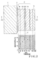
- Fig. 2 shows a section of a main part of an image pickup tube target according to an embodiment of the present invention, and a diagram of a Se-As-Te concentration distribution.
- Figs. 1 and 2 the same reference numerals are used to denote the same parts, a detailed description of which will be omitted.
- the layer 4d comprises a P-type Se-As amorphous semiconductor film having a concentration distribution such that the Se concentration is 75 ⁇ 5 wt% and the As concentration is 25 ⁇ 5 wt%.
- a fourth P-type photoconductive layer 4e serving as a capacitive layer is formed on the rear major surface of the third P-type photoconductive layer 4d to have a thickness such that a multilayer film 4' has a total thickness of, for example, about 3900 nm.
- the fourth P-type photoconductive layer 4e comprises a P-type Se-As amorphous semiconductor film having a concentration such that the Se concentration is 97 t 2 wt% and the As concentration is 3 ⁇ 2 wt%.
- In 2 0 3 having negative space charges in selenium is doped to a thickness of 3 to 30 nm at a concentration of 100 to 3,000 wtppm across an interface between the third and fourth P-type photoconductive layers 4d and 4e, so that an In 2 0 3 -doped layer 4f is formed not to contact the Te layer of the second P-type photoconductive layer 4b.
- the layer 4f is illustrated as doped with In 2 0 3 , other dopants such as MoO 2 or a mixture of In 2 0 3 and MoO 2 which have negative space charges in selenium may also be used.
- the arsenic content (concentration x thickness) in the third P-type photoconductive layer 4d as the carrier extraction layer is decreased to 1/3 to 1/6 of that of the conventional image pickup tube target.
- the doped layer 4f of In 2 0 3 , MoO 2 or mixture thereof which has negative space charges in selenium and which has carrier extraction capability is formed across the interface between the third and fourth P-type photoconductive layers 4d and 4e, so that the carrier extraction efficiency is greatly improved and the sticking phenomenon can be greatly decreased.
- the arsenic content of the carrier extracton layer is decreased to about 1/6 or lower, the effect for preventing tellurium from being diffused from the second P-type photoconductive layer 4b is impaired. Therefore, the arsenic content in a rectangular concentration distribution cannot be decreased to about 1/6 or lower.
- Fig. 3 shows the relation between the position of the indium-doped layer 4f and the sticking contrast for various In 2 0 3 doping contents (wtppm.nm) as defined by concentration y (wtppm) x thickness x (nm).
- Curves 1 to 4 correspond to doping contents of 90000 wtppm ⁇ nm (3000 wtppm x 30 nm), 15000 wtppm ⁇ nm (1000 wtppm x 15 nm), 8000 wtppm-nm (750 wtppm x 12 nm) and 300 wtppm ⁇ nm (100 wtppm x 3 nm), respectively.
- Points Pl, P2 and P3 correspond to positions of the indium-doped layer as shown in Figs. 4a, 4b and 4c, respectively. It will then be appreciated that when the indium-doped layer is formed across the interface X, preferably, substantially centered to the interface X, all the characteristic curves 1 to 4 representative of 100 to 3000 wtppm In 2 0 3 doping concentrations and 3 to 30 nm indium-doped layer thicknesses fall in an allowable sticking contrast range as hatched.
- the In 2 0 3 layer is formed in a thickness region having as a center the interface or boundary X where the arsenic content (25 t 5 wt%) of the third P-type photoconductive layer 4d is abruptly decreased to the arsenic content (3 ⁇ 2 wt%) of the fourth P-type photoconductive layer 4e.
- the arsenic content gradually decreases as shown at solid line or dotted line in Fig. 5.
- the In 2 0 3 layer may be formed in a thickness region having as a center a point where the arsenic concentration of the third P-type photoconductive layer 4d is decreased to 10% of an arsenic concentration difference between the third and fourth P-type photoconductive layers 4d and 4e.
- the total thickness of P-type photoconductive layer 4' is not limited to 3900 nm and the effects of the present invention can be attained irrespective of the total thickness.
- the total thickness may be 5900 nm with the photoconductive layer 5 ending at 6000 nm.
- MoO 2 or a mixture thereof is doped in a highlight sticking prevention Saticon film (Japanese Patent Application No. 55-157084) doped with Li-F across an interface between the first and second P-type photoconductive layers 4a and 4b as shown at dotted line in Fig. 2, to form a doped layer 4f.
- a highlight sticking prevention Saticon film Japanese Patent Application No. 55-157084
- Li-F across an interface between the first and second P-type photoconductive layers 4a and 4b as shown at dotted line in Fig. 2
- the sticking phenomenon can be prevented in the same manner as in the above embodiment.
- the sticking phenomenon which results from photographing of a highly luminous object can also be suppressed
- the sticking phenomenon due to highly luminous incident light can be greatly decreased to obtain a high-quality image.
Landscapes
- Physics & Mathematics (AREA)
- Electromagnetism (AREA)
- Image-Pickup Tubes, Image-Amplification Tubes, And Storage Tubes (AREA)
Applications Claiming Priority (2)
| Application Number | Priority Date | Filing Date | Title |
|---|---|---|---|
| JP5915/83 | 1983-01-19 | ||
| JP591583A JPS59132541A (ja) | 1983-01-19 | 1983-01-19 | 撮像管タ−ゲツト |
Publications (3)
| Publication Number | Publication Date |
|---|---|
| EP0114652A2 true EP0114652A2 (de) | 1984-08-01 |
| EP0114652A3 EP0114652A3 (en) | 1984-08-08 |
| EP0114652B1 EP0114652B1 (de) | 1987-09-09 |
Family
ID=11624188
Family Applications (1)
| Application Number | Title | Priority Date | Filing Date |
|---|---|---|---|
| EP19840100470 Expired EP0114652B1 (de) | 1983-01-19 | 1984-01-18 | Target für Bildaufnahmeröhre |
Country Status (3)
| Country | Link |
|---|---|
| EP (1) | EP0114652B1 (de) |
| JP (1) | JPS59132541A (de) |
| DE (1) | DE3466130D1 (de) |
Cited By (2)
| Publication number | Priority date | Publication date | Assignee | Title |
|---|---|---|---|---|
| EP0163468A3 (en) * | 1984-05-21 | 1986-07-09 | Hitachi, Ltd. | A photoconductive film |
| FR2577713A1 (fr) * | 1985-02-20 | 1986-08-22 | Hitachi Ltd | Cible de tube de prise de vues |
Families Citing this family (2)
| Publication number | Priority date | Publication date | Assignee | Title |
|---|---|---|---|---|
| JPS61193335A (ja) * | 1985-02-20 | 1986-08-27 | Hitachi Ltd | 撮像管タ−ゲツト |
| JPS63299035A (ja) * | 1987-05-29 | 1988-12-06 | Sony Corp | 非晶質セレンを主体とする光導電膜 |
Family Cites Families (2)
| Publication number | Priority date | Publication date | Assignee | Title |
|---|---|---|---|---|
| JPS5832454B2 (ja) * | 1979-06-07 | 1983-07-13 | 日本放送協会 | 光導電性タ−ゲツト |
| JPS57197876A (en) * | 1981-05-29 | 1982-12-04 | Nippon Hoso Kyokai <Nhk> | Photoconductive film |
-
1983
- 1983-01-19 JP JP591583A patent/JPS59132541A/ja active Granted
-
1984
- 1984-01-18 DE DE8484100470T patent/DE3466130D1/de not_active Expired
- 1984-01-18 EP EP19840100470 patent/EP0114652B1/de not_active Expired
Cited By (2)
| Publication number | Priority date | Publication date | Assignee | Title |
|---|---|---|---|---|
| EP0163468A3 (en) * | 1984-05-21 | 1986-07-09 | Hitachi, Ltd. | A photoconductive film |
| FR2577713A1 (fr) * | 1985-02-20 | 1986-08-22 | Hitachi Ltd | Cible de tube de prise de vues |
Also Published As
| Publication number | Publication date |
|---|---|
| EP0114652B1 (de) | 1987-09-09 |
| EP0114652A3 (en) | 1984-08-08 |
| DE3466130D1 (en) | 1987-10-15 |
| JPS59132541A (ja) | 1984-07-30 |
| JPH0522328B2 (de) | 1993-03-29 |
Similar Documents
| Publication | Publication Date | Title |
|---|---|---|
| EP0005543A1 (de) | Fotosensor | |
| EP0067015B1 (de) | Photoleitender Film | |
| EP0114652A2 (de) | Target für Bildaufnahmeröhre | |
| US4587456A (en) | Image pickup tube target | |
| EP0033230B1 (de) | Festkörper-Bildaufnahmevorrichtung | |
| US4330733A (en) | Photoconductive target | |
| US4563611A (en) | Image pick-up tube target | |
| US4617248A (en) | Doped photoconductive film including selenium and tellurium | |
| US4816715A (en) | Image pick-up tube target | |
| JPS6222546B2 (de) | ||
| EP0254136B1 (de) | Target für Bildaufnahmeröhre | |
| US4445131A (en) | Photoconductive image pick-up tube target | |
| US4219831A (en) | Targets for use in photoconductive image pickup tubes | |
| EP0238849B1 (de) | Target für Bildaufnahmeröhre | |
| US4717854A (en) | Image pick-up tube target | |
| JPS61183839A (ja) | 光導電膜 | |
| JPS6310533B2 (de) | ||
| JPS63211545A (ja) | 光導電膜 | |
| JPS62264677A (ja) | 光導電素子 | |
| JPS63299035A (ja) | 非晶質セレンを主体とする光導電膜 | |
| JPS59132538A (ja) | 撮像管タ−ゲツトの形成方法 | |
| JPH07101769B2 (ja) | 半導体レーザ | |
| JPH0152857B2 (de) | ||
| JPS61193336A (ja) | 撮像管タ−ゲツト | |
| GB1532267A (en) | Photoconductive films |
Legal Events
| Date | Code | Title | Description |
|---|---|---|---|
| PUAI | Public reference made under article 153(3) epc to a published international application that has entered the european phase |
Free format text: ORIGINAL CODE: 0009012 |
|
| PUAL | Search report despatched |
Free format text: ORIGINAL CODE: 0009013 |
|
| AK | Designated contracting states |
Designated state(s): DE FR NL |
|
| AK | Designated contracting states |
Designated state(s): DE FR NL |
|
| 17P | Request for examination filed |
Effective date: 19850206 |
|
| 17Q | First examination report despatched |
Effective date: 19860421 |
|
| GRAA | (expected) grant |
Free format text: ORIGINAL CODE: 0009210 |
|
| AK | Designated contracting states |
Kind code of ref document: B1 Designated state(s): DE FR NL |
|
| REF | Corresponds to: |
Ref document number: 3466130 Country of ref document: DE Date of ref document: 19871015 |
|
| ET | Fr: translation filed | ||
| PLBE | No opposition filed within time limit |
Free format text: ORIGINAL CODE: 0009261 |
|
| STAA | Information on the status of an ep patent application or granted ep patent |
Free format text: STATUS: NO OPPOSITION FILED WITHIN TIME LIMIT |
|
| 26N | No opposition filed | ||
| PG25 | Lapsed in a contracting state [announced via postgrant information from national office to epo] |
Ref country code: NL Effective date: 19890801 |
|
| NLV4 | Nl: lapsed or anulled due to non-payment of the annual fee | ||
| PGFP | Annual fee paid to national office [announced via postgrant information from national office to epo] |
Ref country code: FR Payment date: 19921223 Year of fee payment: 10 |
|
| PG25 | Lapsed in a contracting state [announced via postgrant information from national office to epo] |
Ref country code: FR Effective date: 19940930 |
|
| REG | Reference to a national code |
Ref country code: FR Ref legal event code: ST |
|
| PGFP | Annual fee paid to national office [announced via postgrant information from national office to epo] |
Ref country code: DE Payment date: 20030131 Year of fee payment: 20 |