EP0115131A2 - Transistor de type MIS comportant une isolation déposée et enterrée et procédé pour sa fabrication - Google Patents
Transistor de type MIS comportant une isolation déposée et enterrée et procédé pour sa fabrication Download PDFInfo
- Publication number
- EP0115131A2 EP0115131A2 EP83307327A EP83307327A EP0115131A2 EP 0115131 A2 EP0115131 A2 EP 0115131A2 EP 83307327 A EP83307327 A EP 83307327A EP 83307327 A EP83307327 A EP 83307327A EP 0115131 A2 EP0115131 A2 EP 0115131A2
- Authority
- EP
- European Patent Office
- Prior art keywords
- insulating film
- forming
- region
- element forming
- forming region
- Prior art date
- Legal status (The legal status is an assumption and is not a legal conclusion. Google has not performed a legal analysis and makes no representation as to the accuracy of the status listed.)
- Granted
Links
Images





Classifications
-
- H—ELECTRICITY
- H10—SEMICONDUCTOR DEVICES; ELECTRIC SOLID-STATE DEVICES NOT OTHERWISE PROVIDED FOR
- H10D—INORGANIC ELECTRIC SEMICONDUCTOR DEVICES
- H10D30/00—Field-effect transistors [FET]
- H10D30/60—Insulated-gate field-effect transistors [IGFET]
-
- H—ELECTRICITY
- H10—SEMICONDUCTOR DEVICES; ELECTRIC SOLID-STATE DEVICES NOT OTHERWISE PROVIDED FOR
- H10D—INORGANIC ELECTRIC SEMICONDUCTOR DEVICES
- H10D64/00—Electrodes of devices having potential barriers
- H10D64/01—Manufacture or treatment
- H10D64/013—Manufacture or treatment of electrodes having a conductor capacitively coupled to a semiconductor by an insulator
- H10D64/01302—Manufacture or treatment of electrodes having a conductor capacitively coupled to a semiconductor by an insulator the insulator being formed after the semiconductor body, the semiconductor being silicon
- H10D64/01304—Manufacture or treatment of electrodes having a conductor capacitively coupled to a semiconductor by an insulator the insulator being formed after the semiconductor body, the semiconductor being silicon characterised by the conductor
- H10D64/01326—Aspects related to lithography, isolation or planarisation of the conductor
-
- H—ELECTRICITY
- H10—SEMICONDUCTOR DEVICES; ELECTRIC SOLID-STATE DEVICES NOT OTHERWISE PROVIDED FOR
- H10W—GENERIC PACKAGES, INTERCONNECTIONS, CONNECTORS OR OTHER CONSTRUCTIONAL DETAILS OF DEVICES COVERED BY CLASS H10
- H10W10/00—Isolation regions in semiconductor bodies between components of integrated devices
- H10W10/01—Manufacture or treatment
- H10W10/011—Manufacture or treatment of isolation regions comprising dielectric materials
- H10W10/014—Manufacture or treatment of isolation regions comprising dielectric materials using trench refilling with dielectric materials, e.g. shallow trench isolations
-
- H—ELECTRICITY
- H10—SEMICONDUCTOR DEVICES; ELECTRIC SOLID-STATE DEVICES NOT OTHERWISE PROVIDED FOR
- H10W—GENERIC PACKAGES, INTERCONNECTIONS, CONNECTORS OR OTHER CONSTRUCTIONAL DETAILS OF DEVICES COVERED BY CLASS H10
- H10W10/00—Isolation regions in semiconductor bodies between components of integrated devices
- H10W10/10—Isolation regions comprising dielectric materials
- H10W10/17—Isolation regions comprising dielectric materials formed using trench refilling with dielectric materials, e.g. shallow trench isolations
Definitions
- This invention relates to a MIS transistor having a deposited and buried isolation, and a method for manufacturing the same.
- Japanese Patent Disclosure (KOKAI) No. 57-170547 discloses a MIS transistor having a deposited and buried isolation.
- a MIS transistor comprises: a semiconductor substrate 10 with an element forming region 12 formed therein; an insulating film 16 for isolating a device which is deposited and buried in a recessed portion 14 surrounding said device forming region 12; a gate insulating film 18; and a gate electrode 20.
- the gate electrode 20 is located on the insulating film 16 for isolating a device and has a gate fringe portion.
- the MIS transistor is miniaturized, for example; when the gate width becomes 1.0 pm or less, the inverse narrow channel effect indicated by curve a of Fig. 2 occurs. Due to this occurrence, a phenomenon wherein there is a reduced threshold voltage Vt may be observed, so that the threshold voltage Vt cannot be suitably ccontrolled.
- U.S. P. No. 4,160,987 and Japanese Patent Publication No. 57-1145 disclose FETs with nonoverlapping gates.
- the device isolation insulating film 14 of U.S.P. No. 4,160,987 is different from the present invention, since it is formed by thermal oxidization.
- a bird's beak 22 such as that shown in Fig. 3, is formed.
- the present invention is intended to eliminate the inverse narrow channel effect, as indicated by the curve a of Fig. 2.
- One object of the present invention is to provide a MIS transistor in which no fluctuation of the threshold voltage occurs as a result of a decrease in the gate width.
- Another object of this invention is to provide a method of manufacturing a MIS transistor in which no fluctuation of the threshold voltage occurs as a result of a decrease in the gate width.
- the MIS transistor having a deposited and buried isolation, which comprises a semiconductor substrate, an element forming region formed on the semiconductor substrate, said element forming region having a source region, drain region and channel region, an insulating film deposited on and buried within the semiconductor substrate, to surround the element forming region, a gate insulating film formed on the channel region, and a gate electrode formed on the gate insulating film, said gate electrode existing only on the element forming region, the edge portion in the direction of the channel width of the gate electrode being substantially aligned with the edge of the element forming region.
- the concentration of the electric fields at the corners of the element forming region is eliminated, so that the inverse narrow channel effect can be prevented. Therefore, the change in the threshold voltage Vt which results from a gate width can be eliminated.
- the area of the gate electrode is reduced, causing the stray capacitance to be reduced.
- the reduction of the stray capacitance allows the switching time to be shortened, thereby enabling a high-speed operation.
- the present invention since no gate electrode exists on the element isolating region, there is no need for a gap to prevent the contact between the gate electrodes of the adjacent transistors. As a result, the limitation given to the pattern design by the gate electrode is eliminated, which allows the device to be highly integrated.
- a method for manufacturing a MIS transistor having a deposited and buried isolation according to the present invention comprises the steps of:
- the gate electrode can be self-aligned with the element forming region. Therefore, even when no gate fringe is provided, the gate electrode can be completely bridged between the source and drain.
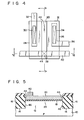
- a P-type semiconductor substrate 10 comprises an element forming region 12 and a recessed portion 14 surrounding the element forming region 12.
- the recessed portion 14 is formed by etching the semiconductor substrate 10.
- a CVD Si0 2 film 16 as an element isolation film is deposited in the recessed portion 14. Since the element isolation film is not formed by the thermally oxidization, no bird's beak will occur.
- N +- type source and drain regions 24 and 26 are formed in the element forming region 12.
- the P-type semiconductor substrate 10 sandwiched by the source and drain regions 24, 26 becomes a channel region 28.
- a gate insulating film 18 is formed on the channel region 28, with a gate electrode 20 being formed on the gate insulating film 18.
- the source region 24 is connected to a wiring configuration 32, via a contact hole 30, and the drain region 26 is connected to another wiring configuration 36, via another contact hole 34.
- the gate electrode 20 is connected to a wiring configuration 40 via a contact 38. This wiring configuration 40 and the source and drain regions 24, 26 are electrically insulated by an Si0 2 insulating film 42.
- the gate electrode 20 exists only on the element forming region 12.
- An edge portion 44 in the direction of a channel width of the gate electrode is substantially aligned with an edge portion 46 of the element forming region.
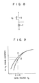
- a dynamic memory such as that shown in Fig. 8 is constituted by using a MIS transistor 0 and a capacitor C.
- V G denotes a voltage to be applied to the gate of the MIS transistor
- I D represents a drain current flowing through the MIS transistor.
- the curve 6 of Fig. 9 indicates the V G -I D characteristic when no inverse narrow channel effect occurs.
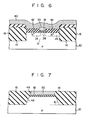
- the slope 6 of the wall surface 46 in the direction of the channel width of the element forming region 12 coincides with the slope 0 of the wall surface 44 in the direction of the channel width of the gate electrode 20, the inverse narrow channel effect can be effectively eliminated.
- the above-mentioned slope e should not be smaller than 45° and not larger than 90°, as shown in Fig. 7.
- a considerable inverse narrow channel effect occurs when the channel width is not larger than 1.0 p. Therefore, when the present invention is applied to a device whose channel width is not larger than 1 . 0 p, a considerable benefit to be derived will consist of the elimination of such an inverse narrow channel effect.
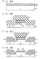
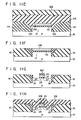
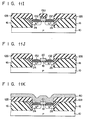
- FIG. 10A to 10K correspond to a cross-sectional view in the direction of line V-V of F ig. 4
- Figs. 11A to 11K correspond to a cross-sectional view in the direction of line VI-VI of Fig. 4.
- a P-type silicon substrate 10 is prepared whose crystal plane is (1, 0, 0) and which has a specific resistance of 5 to 50 ⁇ cm.
- an oxide film 102 is formed over the whole surface on the substrate 10, and a polysilicon film 104 is further deposited on the oxide film 102.
- a resist film is formed over the whole surface and this resist film is patterend to form a resist film pattern 106.
- the polysilicon film 104, oxide film 102 and silicon substrate 10 are etched, by using the resist film pattern 106 as a mask, thereby forming a polysilicon pattern 108, an oxide film pattern 110, the element forming region 12 and the recessed portion 14.
- an Si0 2 film 112 is deposited over the entire surface by the plasma CVD method.
- the Si0 2 film 112 is etched by, e.g., an ammonium fluoride solution. Since the etching rate on the stepped portion of the Si0 2 film 112 is one digit larger than the etching rate on the flat portion of the Si0 2 film 112, as shown in Figs. 10C and 11C, the Si0 2 film 112 is separated into an Si0 2 film 114 in the recessed portion and an Si0 2 film 116 on the element forming region 12. Thereafter the Si0 2 film l16 is removed by the lift-off method.
- an ammonium fluoride solution Since the etching rate on the stepped portion of the Si0 2 film 112 is one digit larger than the etching rate on the flat portion of the Si0 2 film 112, as shown in Figs. 10C and 11C, the Si0 2 film 112 is separated into an Si0 2 film 114 in the recessed portion and an Si0 2 film 116 on the element forming region 12. Thereafter the Si0 2 film l16 is removed by the
- the resist film pattern 106 is removed by a mixed solution of, e.g., sulfuric acid and hydrogen peroxide, and the Si0 2 film 116 is also removed in the same manner (Figs. 10D and 11D).
- a mixed solution of, e.g., sulfuric acid and hydrogen peroxide e.g., sulfuric acid and hydrogen peroxide
- the Si0 2 film 116 is also removed in the same manner (Figs. 10D and 11D).
- an Si0 2 film 118 is deposited over the entire surface by the CVD method, thereby completely burying a V-shaped groove 120 by the Si0 2 film 118.
- a resist film 122 having a fluidity is further formed on it, thereby making the surface flat.
- reactive ion etching for example, is carried out over the entire surface.
- This reactive ion etching is executed under condition wherein the etching rates of the resist film 122 and Si0 2 film 118 are equal, being determined by suitably selecting the thermal treatment time of the resist film 122. Reactive ion etching is performed until the polysilicon pattern 108 is exposed (Figs. 10F and 11F), so that the element isolation film 16 may be formed. Next, a silicon nitride film is formed over the entire surface and is patterned, thereby forming a silicon nitride film pattern 124. The polysilicon pattern 108 and oxide film pattern 110 are etched by using the silicon nitiride film pattern 124 as a mask, to form the gate electrode 20 and the gate insulating film 18.
- N-type impurities are introduced, to form the source and drain regions 24, 26 as well as the channel region 28 (Figs. 10G and 11G).
- an Si0 2 film 126 is deposited over the entire surface by the CVD method.
- the Si0 2 film 126 at the stepped portion is removed by slightly etching the whole surface using hydrogen fluoride HF, so that it is separated into an Si0 2 film 128 on the element isolation film 16, an Si 02 film 130 on the silicon nitiride film pattern 124, and an Si0 2 film 132 on the source and drain regions.
- the silicon nitride film pattern 124 is etched, thereby removing the S i0 2 film 130 (Figs.
- the entire surface is mildly etched by hydrogen fluoride and Al is deposited and patterned, to form the gate wiring 40. Additionally, the source and drain wirings 32, 36 to be connected to the source and drain regions 24 and 26 are also formed (not shown).
- An Ae film may be used in place of the resist film pattern 106, to form the element forming region 12. Furthermore, it is also possible to employ various other methods which is disclosed in Japanese Patent Disclosure (KOKAI) No. 57-170547.
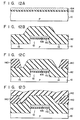
- FIG. 12A After impurities for adjustment of the threshold voltage Vt are introduced to the P-type silicon substrate 10, an oxide film 102 is formed over the entire surface of the substrate 10, and a polysilicon film 104 is further deposited on the oxide film 102.
- a resist film is formed on the polysilicon film 104, being patterned in such a way as to form a mask.
- the polysilicon film 104, oxide film 102 and silicon substrate 10 are etched by using the above-mentioned mask, thereby forming the polysilicon pattern 108, oxide film pattern 110, element forming region 12, and recessed portion 14.
- the Si0 2 film 112 is deposited over the entire surface by the plasma CVD method (Fig. 12B). Thereafter, a resist film is deposited over the entire surface, as shown in Fig. 12C, and is patterned in such a way as to remove only the resist film on the element forming region 12, thereby forming a resist film pattern 140. Furthermore, as shown in Fig. 12D, another resist film 142 is formed over the entire surface, thereby making the surface flat.
- the resist film pattern 140 and the resist film 142 consist of PMMA (polymethyl methacrylate) and OFPR (a trade name of the Tokyo Ooka Co., Ltd).
- a proper mixing ratio of the above two chemical components allows the etching rates of the resist films to coincide with the etching rate of the CVD-Si0 2 film 112.
- reactive dry etching may then be carried out under conditions wherein the etching rates of the Si0 2 film 112, resist film pattern 140 and resist film 142 are equal, thereby exposing the polysilicon pattern 108.
- the element isolation film 16 is formed. Since the subsequent steps are similar to those which have already been mentioned with reference to the first embodiment, a detailed description thereof is omitted.
- FIG. 13A After the impurities for adjustment of the threshold voltage Vt are introduced to the P-type silicon substrate 10, the oxide film 102 is formed over the entire surface of the substrate 10, and the polysilicon film 104 is further deposited on the oxide film 102.
- a resist film is formed on the polysilicon film 104 and is patterned in such a way as to form a mask.
- the polysilicon film 104, oxide film 102 and silicon substrate 10 are etched by using the above-mentioned mask, to form the polysilicon pattern 108, oxide film pattern 110, element forming region 12 and recessed portion 14 (Fig. 13B).
- the Si0 2 film l12 is deposited over the entire surface by the plasma CVD method (Fig. 13C). Thereafter, as shown in Fig. 13D, a resist film is deposited over the entire surface and only the resist film on the element forming region 12 is removed, to form a resist film pattern 150.
- the Si0 2 film 112 on the element forming region 12 is selectively removed (Fig. 13E).
- an Si0 2 film 152 is formed over the entire surface by the CVD method and a resist film 154 is further formed thereon, thereby making the surface flat.
- the present invention is not limited to the above- described embodiments.
- the above-mentioned gate electrode material is not limited to a polysilicon, but may be a metal such as At, or an alloy such as Mo-Si.
- the above-mentioned insulating film for isolating elements is not limited to a CVD-Si0 2 film; similarly, the gate insulating film is not limited to a thermally oxidized film.
- many other modifications and variations are possible, without departing from the spirit and intended scope of the invention.
Landscapes
- Insulated Gate Type Field-Effect Transistor (AREA)
- Local Oxidation Of Silicon (AREA)
Applications Claiming Priority (2)
| Application Number | Priority Date | Filing Date | Title |
|---|---|---|---|
| JP57233419A JPS59123266A (ja) | 1982-12-28 | 1982-12-28 | Misトランジスタ及びその製造方法 |
| JP233419/82 | 1982-12-28 |
Publications (3)
| Publication Number | Publication Date |
|---|---|
| EP0115131A2 true EP0115131A2 (fr) | 1984-08-08 |
| EP0115131A3 EP0115131A3 (en) | 1986-12-10 |
| EP0115131B1 EP0115131B1 (fr) | 1989-09-13 |
Family
ID=16954763
Family Applications (1)
| Application Number | Title | Priority Date | Filing Date |
|---|---|---|---|
| EP83307327A Expired EP0115131B1 (fr) | 1982-12-28 | 1983-12-01 | Transistor de type MIS comportant une isolation déposée et enterrée et procédé pour sa fabrication |
Country Status (3)
| Country | Link |
|---|---|
| EP (1) | EP0115131B1 (fr) |
| JP (1) | JPS59123266A (fr) |
| DE (1) | DE3380581D1 (fr) |
Cited By (4)
| Publication number | Priority date | Publication date | Assignee | Title |
|---|---|---|---|---|
| FR2568723A1 (fr) * | 1984-08-03 | 1986-02-07 | Commissariat Energie Atomique | Circuit integre notamment de type mos et son procede de fabrication |
| EP0388564A3 (fr) * | 1988-02-11 | 1993-10-06 | STMicroelectronics, Inc. | Procédé de la formation d'une structure non planaire sur un substrat semi-conducteur |
| WO1997020336A3 (fr) * | 1995-11-30 | 1997-08-28 | Siemens Ag | Procede de fabrication d'un dispositif a circuits integres equipe d'au moins un transistor mos |
| US6452287B1 (en) * | 1999-06-14 | 2002-09-17 | Ivan Looker | Windmill and method to use same to generate electricity, pumped air or rotational shaft energy |
Family Cites Families (9)
| Publication number | Priority date | Publication date | Assignee | Title |
|---|---|---|---|---|
| IN140846B (fr) * | 1973-08-06 | 1976-12-25 | Rca Corp | |
| JPS5379383A (en) * | 1976-12-24 | 1978-07-13 | Toshiba Corp | Production of semiconductor device |
| JPS5397380A (en) * | 1977-02-07 | 1978-08-25 | Toshiba Corp | Manufacture of semiconductor device |
| US4222792A (en) * | 1979-09-10 | 1980-09-16 | International Business Machines Corporation | Planar deep oxide isolation process utilizing resin glass and E-beam exposure |
| US4333794A (en) * | 1981-04-07 | 1982-06-08 | International Business Machines Corporation | Omission of thick Si3 N4 layers in ISA schemes |
| CA1165014A (fr) * | 1981-04-13 | 1984-04-03 | Kei Kurosawa | Methode de fabrication d'un semiconducteur |
| JPS57176742A (en) * | 1981-04-21 | 1982-10-30 | Nippon Telegr & Teleph Corp <Ntt> | Semiconductor device and manufacture thereof |
| JPS5848936A (ja) * | 1981-09-10 | 1983-03-23 | Fujitsu Ltd | 半導体装置の製造方法 |
| JPS58165341A (ja) * | 1982-03-26 | 1983-09-30 | Toshiba Corp | 半導体装置の製造方法 |
-
1982
- 1982-12-28 JP JP57233419A patent/JPS59123266A/ja active Pending
-
1983
- 1983-12-01 EP EP83307327A patent/EP0115131B1/fr not_active Expired
- 1983-12-01 DE DE8383307327T patent/DE3380581D1/de not_active Expired
Cited By (6)
| Publication number | Priority date | Publication date | Assignee | Title |
|---|---|---|---|---|
| FR2568723A1 (fr) * | 1984-08-03 | 1986-02-07 | Commissariat Energie Atomique | Circuit integre notamment de type mos et son procede de fabrication |
| WO1986001336A1 (fr) * | 1984-08-03 | 1986-02-27 | Commissariat A L'energie Atomique | Procede de fabrication d'un circuit integre de type mis |
| EP0388564A3 (fr) * | 1988-02-11 | 1993-10-06 | STMicroelectronics, Inc. | Procédé de la formation d'une structure non planaire sur un substrat semi-conducteur |
| WO1997020336A3 (fr) * | 1995-11-30 | 1997-08-28 | Siemens Ag | Procede de fabrication d'un dispositif a circuits integres equipe d'au moins un transistor mos |
| US6037196A (en) * | 1995-11-30 | 2000-03-14 | Siemens Aktiengesellschaft | Process for producing an integrated circuit device with at least one MOS transistor |
| US6452287B1 (en) * | 1999-06-14 | 2002-09-17 | Ivan Looker | Windmill and method to use same to generate electricity, pumped air or rotational shaft energy |
Also Published As
| Publication number | Publication date |
|---|---|
| EP0115131A3 (en) | 1986-12-10 |
| JPS59123266A (ja) | 1984-07-17 |
| EP0115131B1 (fr) | 1989-09-13 |
| DE3380581D1 (en) | 1989-10-19 |
Similar Documents
| Publication | Publication Date | Title |
|---|---|---|
| US5786263A (en) | Method for forming a trench isolation structure in an integrated circuit | |
| KR100306935B1 (ko) | 집적회로내에트렌치절연구조물을형성하는방법 | |
| US6524931B1 (en) | Method for forming a trench isolation structure in an integrated circuit | |
| US3475234A (en) | Method for making mis structures | |
| JP3468294B2 (ja) | シリコンオンインシュレータ・ボディコンタクトを形成する方法およびボディコンタクト構造 | |
| US3943542A (en) | High reliability, low leakage, self-aligned silicon gate FET and method of fabricating same | |
| US20020005581A1 (en) | Semiconductor device having an insulated gate and a fabrication process thereof | |
| US5067000A (en) | Semiconductor device having field shield isolation | |
| US4316203A (en) | Insulated gate field effect transistor | |
| US4523368A (en) | Semiconductor devices and manufacturing methods | |
| EP0115131B1 (fr) | Transistor de type MIS comportant une isolation déposée et enterrée et procédé pour sa fabrication | |
| US3829888A (en) | Semiconductor device and the method of making the same | |
| KR19990064136A (ko) | 기판에 트랜치 절연을 형성하는 방법 | |
| US4060827A (en) | Semiconductor device and a method of making the same | |
| EP0268472B1 (fr) | Transistors à induction statique à grille isolée formée sur la paroi d'un sillon et leur procédé de fabrication | |
| JP3127253B2 (ja) | Soi型半導体装置およびその製造方法 | |
| JPH04146665A (ja) | 抵抗素子 | |
| KR100197656B1 (ko) | 반도체 에스.오.아이.소자의 제조방법 | |
| KR100192973B1 (ko) | 경사진 게이트 산화막을 갖는 전력용 모스 소자및그제조방법 | |
| JPH0298939A (ja) | 半導体装置の製造方法 | |
| JPH05129335A (ja) | 縦型トランジスタの製造方法 | |
| JPH0621369A (ja) | Mos集積回路の製造方法 | |
| US6274517B1 (en) | Method of fabricating an improved spacer | |
| KR0161118B1 (ko) | 반도체 소자 제조방법 | |
| US4138781A (en) | Method for manufacturing semiconductor device |
Legal Events
| Date | Code | Title | Description |
|---|---|---|---|
| PUAI | Public reference made under article 153(3) epc to a published international application that has entered the european phase |
Free format text: ORIGINAL CODE: 0009012 |
|
| 17P | Request for examination filed |
Effective date: 19831212 |
|
| AK | Designated contracting states |
Designated state(s): DE FR GB |
|
| RAP1 | Party data changed (applicant data changed or rights of an application transferred) |
Owner name: KABUSHIKI KAISHA TOSHIBA |
|
| PUAL | Search report despatched |
Free format text: ORIGINAL CODE: 0009013 |
|
| AK | Designated contracting states |
Kind code of ref document: A3 Designated state(s): DE FR GB |
|
| 17Q | First examination report despatched |
Effective date: 19880603 |
|
| GRAA | (expected) grant |
Free format text: ORIGINAL CODE: 0009210 |
|
| AK | Designated contracting states |
Kind code of ref document: B1 Designated state(s): DE FR GB |
|
| REF | Corresponds to: |
Ref document number: 3380581 Country of ref document: DE Date of ref document: 19891019 |
|
| ET | Fr: translation filed | ||
| PLBE | No opposition filed within time limit |
Free format text: ORIGINAL CODE: 0009261 |
|
| STAA | Information on the status of an ep patent application or granted ep patent |
Free format text: STATUS: NO OPPOSITION FILED WITHIN TIME LIMIT |
|
| 26N | No opposition filed | ||
| PGFP | Annual fee paid to national office [announced via postgrant information from national office to epo] |
Ref country code: GB Payment date: 19971124 Year of fee payment: 15 |
|
| PGFP | Annual fee paid to national office [announced via postgrant information from national office to epo] |
Ref country code: DE Payment date: 19971205 Year of fee payment: 15 |
|
| PGFP | Annual fee paid to national office [announced via postgrant information from national office to epo] |
Ref country code: FR Payment date: 19971209 Year of fee payment: 15 |
|
| PG25 | Lapsed in a contracting state [announced via postgrant information from national office to epo] |
Ref country code: GB Free format text: LAPSE BECAUSE OF NON-PAYMENT OF DUE FEES Effective date: 19981201 |
|
| GBPC | Gb: european patent ceased through non-payment of renewal fee |
Effective date: 19981201 |
|
| PG25 | Lapsed in a contracting state [announced via postgrant information from national office to epo] |
Ref country code: FR Free format text: LAPSE BECAUSE OF NON-PAYMENT OF DUE FEES Effective date: 19990831 |
|
| REG | Reference to a national code |
Ref country code: FR Ref legal event code: ST |
|
| PG25 | Lapsed in a contracting state [announced via postgrant information from national office to epo] |
Ref country code: DE Free format text: LAPSE BECAUSE OF NON-PAYMENT OF DUE FEES Effective date: 19991001 |