EP0117604A2 - Elektrooptische Lichtschalter - Google Patents
Elektrooptische Lichtschalter Download PDFInfo
- Publication number
- EP0117604A2 EP0117604A2 EP84300191A EP84300191A EP0117604A2 EP 0117604 A2 EP0117604 A2 EP 0117604A2 EP 84300191 A EP84300191 A EP 84300191A EP 84300191 A EP84300191 A EP 84300191A EP 0117604 A2 EP0117604 A2 EP 0117604A2
- Authority
- EP
- European Patent Office
- Prior art keywords
- electro
- ceramic body
- plzt
- temperature
- optical
- Prior art date
- Legal status (The legal status is an assumption and is not a legal conclusion. Google has not performed a legal analysis and makes no representation as to the accuracy of the status listed.)
- Granted
Links
Images




Classifications
-
- G—PHYSICS
- G02—OPTICS
- G02F—OPTICAL DEVICES OR ARRANGEMENTS FOR THE CONTROL OF LIGHT BY MODIFICATION OF THE OPTICAL PROPERTIES OF THE MEDIA OF THE ELEMENTS INVOLVED THEREIN; NON-LINEAR OPTICS; FREQUENCY-CHANGING OF LIGHT; OPTICAL LOGIC ELEMENTS; OPTICAL ANALOGUE/DIGITAL CONVERTERS
- G02F1/00—Devices or arrangements for the control of the intensity, colour, phase, polarisation or direction of light arriving from an independent light source, e.g. switching, gating or modulating; Non-linear optics
- G02F1/01—Devices or arrangements for the control of the intensity, colour, phase, polarisation or direction of light arriving from an independent light source, e.g. switching, gating or modulating; Non-linear optics for the control of the intensity, phase, polarisation or colour
- G02F1/03—Devices or arrangements for the control of the intensity, colour, phase, polarisation or direction of light arriving from an independent light source, e.g. switching, gating or modulating; Non-linear optics for the control of the intensity, phase, polarisation or colour based on ceramics or electro-optical crystals, e.g. exhibiting Pockels effect or Kerr effect
- G02F1/055—Devices or arrangements for the control of the intensity, colour, phase, polarisation or direction of light arriving from an independent light source, e.g. switching, gating or modulating; Non-linear optics for the control of the intensity, phase, polarisation or colour based on ceramics or electro-optical crystals, e.g. exhibiting Pockels effect or Kerr effect the active material being a ceramic
Definitions
- This invention relates to electro-optical light shutters.
- a PLZT ceramic has the following advantages:
- FIG. 1 of the accompanying drawings is a diagram showing the basic construction of a PLZT electro-optical light shutter apparatus.
- the apparatus comprises linear polarizers 1 and 2 between which an electro-optical light shutter 3 including a PLZT ceramics plate 6 is disposed.
- the electro-optical light shutter 3 comprises a pair of electrodes 4 and 5 disposed on the PLZT plate 6.
- the linear polarizers 1 and 2 are disposed in such a manner that the electric field vector directions of the linearly polarized light selected thereby are perpendicular to each other.
- the PLZT plate 6 is disposed in such a manner that its electric field direction, namely, the optical axis direction is at 45° to each of the former directions.
- Such a PLZT electro-optical shutter has advantages such as high speed, with a response time of microsecond order; it can be made as a full solid state structure; it has long life; and high reliability. Accordingly, such PLZT electro-optical shutters have been proposed for use as a flash brightness prevention shutter, in a viewer in a stereoscopic television system, in a colour television receiver employing a black and white television picture tube as disclosed in Japanese unexamined patent publication no. 57/55685, and in a high brightness projector.
- a parallel stripe filter formed of red, green and blue colour stripes, each extending in, for example, the vertical direction.
- Electro-optical shutter elements are disposed at each stripe in opposing relation to the filter.
- the electron beams are modulated by the colour signals corresponding to red, green and blue colours, and the respective electro-optical shutter element associated with each stripe is alternately made on and off in synchronism therewith.
- the optical image of each of the red, green and blue colours is produced through each stripe filter, and hence a reproduced colour image can be obtained.
- FIG. 2 of the accompanying drawings shows an example of the construction of a high brightness projector to which such a PLZT electro-optical shutter array can be applied.
- a picture of one horizontal scanning line is formed sequentially.
- the light emitted from a light source 11 is projected through a collimator lens 12, an iris 13, a linear polarizer 14, a lens system 15 and a mirror 16 to an electro-optical light shutter 17.
- the light projected onto the shutter 17 is formed by the iris 13 and the lens system 15 into light flux of a slit-shape perpendicular to the plane of Figure 2.
- the shutter 17 comprises PLZT elements which are disposed in stripe shape on a plane at the position irradiated by light flux of slit shape. Then, in response to the video signal of one horizontal scanning line, each PLZT element is sequentially turned on and off and the light passed therethrough is projected through an analyzer 18, a condenser lens 19, a movable mirror 20 and a projection lens 21 onto a screen (not shown).
- the linear polarizer 14 and the analyzer 18 respectively correspond to the linear polarizers 1 and 2 in Figure 2.
- the movable mirror 20 is driven or vibrated along the surface of the sheet in Figure 2, namely, in the horizontal direction shown by arrows, at, for example, one field period.
- the driving of the shutter is carried out at a driving frequency higher than 5 kHz.
- PLZT ceramic is formed of a mixed system of PbZr03, PbTi0 3 and La 2 0 3 and the composition formula thereof is expressed by
- the PLZT ceramic Since its composition is determined by the amounts of La, Zr and Ti, its composition can be expressed by x/y/z.
- the PLZT ceramic is roughly classified into a linear electro-optical effect material which shows Pockels effect as a mode of birefringence caused by electro-optical effect, quadratic electro-optical effect material which shows Kerr effect, and a memory material which shows memory effect.
- a linear electro-optical effect material which shows Pockels effect as a mode of birefringence caused by electro-optical effect
- quadratic electro-optical effect material which shows Kerr effect
- a memory material which shows memory effect.
- Figure 6 of the accompanying drawings shows the ranges of the compositions circled by the solid lines which form the memory effect material, the linear electro-optical effect material and the quadratic electro-optical effect material each having a composition of x/y/z.
- PLZT ceramics for electro-optical light shutters have been selected to have a composition of 9.5 to 9.0/65/35 for quadratic electro-optical effect.
- the reason for this is that the PLZT ceramics having the above composition can exhibit the quadratic effect at ambient temperatures ranging from -20°C to 80 0 C, and can be used in an electro-optical light shutter.
- the temperature characteristic of the quadratic electro-optical coefficient R of the PLZT ceramics has a large negative value, so that in the use at temperatures higher than room temperature the operating voltage is raised and hence the operating electric power is increased, and moreover discharge may occur between the electrodes, so resulting in problems in use.
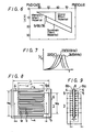
- curves 22, 23 and 24 indicate operating voltage versus output I/I 0 (where 10 represents the incident light intensity and I represents the detected light intensity) for D.C., 500 Hz and 5 kHz operation.
- an electro-optical light shutter comprising:
- an electro-optical light shutter comprising:
- the operating power P of the PLZT ceramic is given as: Since: and: where is the wavelength, d is the distance between the pair of electrodes on the PLZT element, t is the thickness of the PLZT element, & is the length of the electrodes, n is the refractive index of the PLZT ceramic, R is the quadratic electro-optical coefficient, and ⁇ 5 is the relative permittivi ty of the PLZT ceramic.
- equation 2 when d, l, X and f are selected to be constant, it is desired that the coefficient R is as large as possible to enable the PLZT shutter to operate at a low operating voltage and with low power consumption.
- electro-optical light shutter formed of electro-optical ceramic and at least a pair of electrodes through which A.C. voltage is applied to the electro-optical ceramic, for example, a PLZT ceramic
- PLZT ceramics which have memory effect at room temperature and of which the memory effect is substantially lost at a constant elevated temperature caused by the application of the A.C. voltage.
- optical light shutter may additionally be provided with a heating means which holds the PLZT ceramic at the above constant elevated temperature.
- the PLZT ceramic changes to exhibit the quadratic effect at a temperature higher than a critical temperature limit at which the memory effect is no longer exhibited (hereinafter this temperature is referred to as the memory temperature).
- the electro-optical coefficient R has a large value at temperatur es near the memory temperature.
- the PLZT ceramic used for the electro-optical light shutter has a composition which exhibits the memory effect at room temperature and exhibits the quadratic effect at an elevated temperature resulting from heat generated by the A.C. voltage used to drive the shutter plus, possibly, external heating means provided to hold the PLZT ceramic at the elevated temperature.
- the PLZT ceramic is driven at the above condition where it has a high electro-optical coefficient R.
- Raw materials for providing the PLZT ceramic having a desired composition are weighed, mixed by a ball mill at a revolution speed of 60 rpm for 15 hours, filtered, dried at 140°C for 15 hours and temporarily pressed under a pressure of 500 kg/cm 2 .
- This temporarily pressed body is calcined at 900°C for 1 hour, then ground by a ball mill rotating at a revolution speed of 60 rpm for 15 hours, filtered again, dried at 140°C for 15 hours and then pressed under a pressure of It/cm .
- This product is hot pressed at 1250°C for 4 hours under a pressure of 200 kg/cm 7 in an oxygen atmosphere.
- the hot-pressed sintered product thus made is sliced into thin wafers, lapped on both surfaces and then mirror-finished.
- Electrodes are deposited on the plate shaped PLZT ceramic body so formed. An example thereof is shown in Figures 8 and 9.
- the electrodes are deposited by a surface electrode method.
- On each of the major surfaces 6a and 6b of the PLZT plate 6 are deposited a pair of comb- tooth electrodes 4 and 5, the comb teeth of which alternate and are formed parallel to each other.
- a predetermiend operating voltage is applied between the pair of electrodes 4 and 5.
- the electrodes 4 and 5 corresponding to each other on both the major surfaces 6a and 6b, and having the same polarity, are disposed in opposing relation thereto through the PLZT plate 6.
- the electrodes 4 and 5 are formed by a printing method employing silver paste or a metal vacuum deposition in which chromium is deposited to a thickness of 1000 Angstroms, and on which gold is further deposited to have a thickness of 4000°Angstroms.
- a spacing d between the electrodes 4 and 5 on the major surfaces 6a and 6b is increased, while the spacing between the major surfaces 6a and 6b, namely, the thickness t of the PLZT plate 6 is reduced.
- the PLZT plate 6 is made to have a composition which exhibits the memory effect at room temperature as described before.
- the memory temperature of each composition in which the value x is changed was measured and the results thereof are shown by a curve 25 in Figure 10. It was confirmed that the memory effect was present in the temperature region below the curve 25 for each value of x, while the quadratic electro-optical effect was present in the region above the curve 25.
- the applied operating voltage is a DC voltage.
- the measured results of the temperature characteristic of the electro-optical coefficient R for the PLZT ceramic having the composition of x/65/39 when the value of x is changed are shown in Figure 11.
- a helium-neon laser (whose wavelength is 633 nm) was used as the light source and the amount of light from the analyzer, with the construction as shown in Figure 1, was measured.
- the temperature at the left-hand end of each curve represents the memory temperature and a case where the contrast ratio indicates a value larger than 1/10 is regarded as a case which exhibits the memory effect.
- the electro-optical coefficient R indicates the larger value as the temperature becomes closer to the memory temperature.
- the memory effect is exhibited, namely, the contrast ratio exceeds 1/10.
- the distance L 1 between the outer edges of the coupling portions of each comb tooth of the pair of comb tooth electrodes 4 and 5 is 9.6 mm
- the distance L 2 between the inner edges thereof is 8.6 mm
- the length L3 between the tip ends of each comb tooth is 7.6 mm
- the outside width W A of one electrode 4 is 7.6 mm
- the outside width W B of the other electrode 5 is 6.6 mm.
- the space d between the electrodes 4 and 5 is 430 microns
- the comb tooth width W is 120 microns
- the thickness t of the PLZT plate 6 is 300 microns.
- the optimum composition of PLZT ceramic for minimizing the half-wave voltage V ⁇ /2 can be determined.
- the electro-optical light shutter employing the sample No 5 can reduce the operating voltage to 1/3, and the operating power can be reduced to approximately 1/10.
- the operating power is proportional to the square of the operating voltage, since, depending on each composition, the relative permittivity E S and the dielectric loss angle ⁇ differ with the temperature and operating voltage, it cannot simply be taken that the operating power is proportional to the square of the operating voltage.
- heating means which externally sets the temperature in the operation of the PLZT plate 6 at a predetermined temperature independent of the ambient temperature. That is:
- the PLZT temperatures of the samples Nos 1, 2, 3, 4, 5, 6, each having the composition shown in Table 1 in which the ambient temperature is 25 0 C and the operating voltage is selected as 150 V and 200 V, without the heating means were measured.
- the measured results are shown in Table 2.
- the optimum PLZT composition with an ambient room temperature is determined by comparing the graph of Figure 12 and Table 2.
- the composition of the sample No 5 namely, 7.3/65/35 is the best one.
- the temperature of the PLZT ceramic body having the composition of 7.3/65/35 at the operating voltage of 150 V is 86°C, and the half-wave voltage V ⁇ /2 at 86°C becomes 150 V, which then corresponds to each other in Table 2 and the graph of Figure 12. While in this example the ambient temperature is made constant, the environment may actually fluctuate over at least -10°C to 40°, and this must be taken into consideration in a practical apparatus.
- the PLZT temperature is also elevated, thus increasing the operating voltage more.
- the PLZT temperature is changed so that the operation of the electro-optical light shutter becomes impossible and the operating voltage therefor is greatly changed.
- the operating voltage is changed, so that it becomes necessary to temperature compensate the operating voltage in the driving circuit.
- a heating means is provided adjacent to but external to the PLZT plate 6 to hold it at a constant temperature.
- This external heating means can comprise a heater element and a temperature sensor which detects the temperature of the PLZT plate 6 and then controls the heater element to maintain the PLZT plate 6 at a predetermined temperature.
- a transparent substrate 50 made of glass is bonded to the PLZT plate 6 on one surface by an adhesive agent and on the substrate 50 is deposited a transparent resistive layer, for example, of SnO 2 .
- a heater 51 which is formed by a transparent resistive layer having resistivity of 25 ohms/square. Conductive terminals 52 and 53 are depositqd at respective ends of the heater 51 and a voltage is applied across the terminals 52 and 53.
- a temperature detecting element 54 such as a thermistor is disposed in contact with the PLZT plate 6 and by a signal detected by the temperature detecting element 54, the power source circuit (not shown) for the heater 51 is controlled so as to maintain the PLZT plate 6 at a constant temperature, namely, a temperature higher than the memory temperature, for example, 120°C.
- the above temperature detection can also be carried out using a capacitor formed by the PLZT ceramic per se, and the temperature is then detected by changes in the capacitance of the capacitor.
- a pair of electrodes are provided on the PLZT ceramic to form the capacitor, and the heater is controlled in response to the change of the capacitance of the capacitor.
- the heater power was 0.5 W at an ambient temperature of 0°C and zero W at an ambient temperature of 40°C.
- the PLZT plate 6 having the composition of 7.3/65/35 requires a PLZT operating power of 1.5 W at an ambient temperature of 25°C and 2.3 W at an ambient temperature of 40°C.
- the required PLZT operating power was 10.6 W at an ambient temperature of 25°C.
- the electro-optical light shutter described uses a PLZTiceramic body having a characteristic which exhibits the memory effect at room temperature but the quadratic effect at the operating temperature. In this way the operating voltage can be lowered. Moreover, when an external heating means is provided to hold the PLZT temperature constant independent of the ambient temperature, the operating voltage can be made constant and the start-up time of the electro-optical light shutter is reduced, and furthermore, the total power consumption of the shutter can be decreased.
- the operating voltage of the PLZT shutter is lowered, the risk of discharge between the electrodes of the PLZT plate is reduced, the power of the PLZT electro-optical light shutter driving circuit can be reduced, the reliability thereof can be raised, and the manufacturing cost can be decreased.
- the noise level caused by the PLZT ceramic body can be decreased and the long-term reliability of the PLZT ceramic itself can be raised. Furthermore, owing to the reduction of the electric power, a battery can be used as the power source, so permitting use in portable apparatus.
Landscapes
- Physics & Mathematics (AREA)
- Chemical & Material Sciences (AREA)
- Engineering & Computer Science (AREA)
- Ceramic Engineering (AREA)
- Nonlinear Science (AREA)
- Crystallography & Structural Chemistry (AREA)
- General Physics & Mathematics (AREA)
- Optics & Photonics (AREA)
- Optical Modulation, Optical Deflection, Nonlinear Optics, Optical Demodulation, Optical Logic Elements (AREA)
- Devices For Indicating Variable Information By Combining Individual Elements (AREA)
- Mechanical Light Control Or Optical Switches (AREA)
Applications Claiming Priority (2)
| Application Number | Priority Date | Filing Date | Title |
|---|---|---|---|
| JP4513/83 | 1983-01-14 | ||
| JP58004513A JPS59128514A (ja) | 1983-01-14 | 1983-01-14 | 電気光学シヤツタ− |
Publications (3)
| Publication Number | Publication Date |
|---|---|
| EP0117604A2 true EP0117604A2 (de) | 1984-09-05 |
| EP0117604A3 EP0117604A3 (en) | 1986-11-05 |
| EP0117604B1 EP0117604B1 (de) | 1990-10-24 |
Family
ID=11586131
Family Applications (1)
| Application Number | Title | Priority Date | Filing Date |
|---|---|---|---|
| EP84300191A Expired - Lifetime EP0117604B1 (de) | 1983-01-14 | 1984-01-12 | Elektrooptische Lichtschalter |
Country Status (5)
| Country | Link |
|---|---|
| US (1) | US4621903A (de) |
| EP (1) | EP0117604B1 (de) |
| JP (1) | JPS59128514A (de) |
| CA (1) | CA1214534A (de) |
| DE (1) | DE3483431D1 (de) |
Cited By (1)
| Publication number | Priority date | Publication date | Assignee | Title |
|---|---|---|---|---|
| US5177501A (en) * | 1989-11-13 | 1993-01-05 | Alcatel N.V. | Electrooptical recording device |
Families Citing this family (5)
| Publication number | Priority date | Publication date | Assignee | Title |
|---|---|---|---|---|
| JP2570756B2 (ja) * | 1987-08-07 | 1997-01-16 | ミノルタ株式会社 | 光シャッタの駆動方法 |
| US4915481A (en) * | 1988-08-25 | 1990-04-10 | Sperry Marine Inc. | Apparatus for preventing space charge buildup effects in electrically controllable optical transmission cells |
| US5621559A (en) * | 1994-04-18 | 1997-04-15 | California Institute Of Technology | Ferroelectric optical computing device with low optical power non-destructive read-out |
| DE102009028228A1 (de) * | 2009-08-04 | 2011-02-17 | Ball Packaging Europe Gmbh | Vorrichtung und Verfahren zur Oberflächenbearbeitung mit einer Prüfstation |
| KR20120060483A (ko) * | 2010-12-02 | 2012-06-12 | 삼성모바일디스플레이주식회사 | 자외선-오존을 이용한 오염물 세정장치 및 이를 이용한 세정방법 |
Family Cites Families (11)
| Publication number | Priority date | Publication date | Assignee | Title |
|---|---|---|---|---|
| US3666666A (en) * | 1969-12-17 | 1972-05-30 | Atomic Energy Commission | Ferroelectric ceramic materials |
| US3623795A (en) * | 1970-04-24 | 1971-11-30 | Rca Corp | Electro-optical system |
| US3702724A (en) * | 1971-10-13 | 1972-11-14 | Atomic Energy Commission | Ferroelectric ceramic plate electrooptical light scattering device and method |
| US3990770A (en) * | 1972-07-13 | 1976-11-09 | U.S. Philips Corporation | Electro-optic picture display and memory device |
| JPS552852B2 (de) * | 1972-07-31 | 1980-01-22 | ||
| JPS49114436A (de) * | 1973-02-27 | 1974-10-31 | ||
| JPS5544362B2 (de) * | 1974-09-12 | 1980-11-12 | ||
| JPS52113758A (en) * | 1976-03-22 | 1977-09-24 | Hitachi Ltd | Electro-optical device |
| JPS5846470B2 (ja) * | 1976-08-25 | 1983-10-17 | 財団法人小林理学研究所 | 電気光学磁器組成物 |
| JPS5793317A (en) * | 1980-12-02 | 1982-06-10 | Matsushita Electric Ind Co Ltd | Solid-state optical shutter |
| JPS5810717A (ja) * | 1981-07-13 | 1983-01-21 | Ricoh Co Ltd | 光シヤツタ |
-
1983
- 1983-01-14 JP JP58004513A patent/JPS59128514A/ja active Pending
- 1983-12-30 CA CA000444466A patent/CA1214534A/en not_active Expired
-
1984
- 1984-01-04 US US06/568,040 patent/US4621903A/en not_active Expired - Fee Related
- 1984-01-12 DE DE8484300191T patent/DE3483431D1/de not_active Expired - Lifetime
- 1984-01-12 EP EP84300191A patent/EP0117604B1/de not_active Expired - Lifetime
Cited By (1)
| Publication number | Priority date | Publication date | Assignee | Title |
|---|---|---|---|---|
| US5177501A (en) * | 1989-11-13 | 1993-01-05 | Alcatel N.V. | Electrooptical recording device |
Also Published As
| Publication number | Publication date |
|---|---|
| EP0117604A3 (en) | 1986-11-05 |
| CA1214534A (en) | 1986-11-25 |
| DE3483431D1 (de) | 1990-11-29 |
| JPS59128514A (ja) | 1984-07-24 |
| EP0117604B1 (de) | 1990-10-24 |
| US4621903A (en) | 1986-11-11 |
Similar Documents
| Publication | Publication Date | Title |
|---|---|---|
| KR100761236B1 (ko) | 조광 장치와 촬상 장치 및 그 구동 방법 | |
| US5710655A (en) | Cavity thickness compensated etalon filter | |
| US4139278A (en) | Liquid crystal display device | |
| US3820875A (en) | Scanner devices utilizing field effect light scattering dielectrics | |
| EP0117604B1 (de) | Elektrooptische Lichtschalter | |
| US4270847A (en) | Electro-optical light modulation element | |
| US4877310A (en) | Electronically variable MTF filter for image sensor arrays | |
| US5198920A (en) | Transverse pixel format electro-optic spatial light modulator | |
| JPS5987436A (ja) | 光バルブ | |
| JP3241432B2 (ja) | 温度変化検出機能を有する光導電型液晶ライトバルブ表示装置 | |
| GB1374740A (en) | Cathode ray tube display | |
| US3936146A (en) | Irregular ferroelectric element for controllable single domain | |
| JPS59128515A (ja) | 電気光学シヤツタ− | |
| JP2605140B2 (ja) | 光学装置 | |
| US5300928A (en) | Liquid crystal color display device | |
| WO1994027182A9 (en) | Improved liquid crystal light valve | |
| US4095099A (en) | Additive color system with compensation of repeatability errors of variable-density electrooptical filter units | |
| Haertling | PLZT reflective displays | |
| US4088391A (en) | Irregular ferroelectric element devised for single domain-wall motion | |
| US4053207A (en) | Electro-optic devices | |
| JPS6248816B2 (de) | ||
| JP2610205B2 (ja) | 光アドレス型空間光変調装置 | |
| KR0179620B1 (ko) | 광강도 조절장치 | |
| US4229648A (en) | Additive color system with compensation of repeatability errors of variable-density electrooptical filter units | |
| JPS6248814B2 (de) |
Legal Events
| Date | Code | Title | Description |
|---|---|---|---|
| PUAI | Public reference made under article 153(3) epc to a published international application that has entered the european phase |
Free format text: ORIGINAL CODE: 0009012 |
|
| AK | Designated contracting states |
Designated state(s): DE FR GB NL |
|
| PUAL | Search report despatched |
Free format text: ORIGINAL CODE: 0009013 |
|
| AK | Designated contracting states |
Kind code of ref document: A3 Designated state(s): DE FR GB NL |
|
| 17P | Request for examination filed |
Effective date: 19870325 |
|
| 17Q | First examination report despatched |
Effective date: 19890717 |
|
| GRAA | (expected) grant |
Free format text: ORIGINAL CODE: 0009210 |
|
| AK | Designated contracting states |
Kind code of ref document: B1 Designated state(s): DE FR GB NL |
|
| ET | Fr: translation filed | ||
| REF | Corresponds to: |
Ref document number: 3483431 Country of ref document: DE Date of ref document: 19901129 |
|
| PLBE | No opposition filed within time limit |
Free format text: ORIGINAL CODE: 0009261 |
|
| STAA | Information on the status of an ep patent application or granted ep patent |
Free format text: STATUS: NO OPPOSITION FILED WITHIN TIME LIMIT |
|
| 26N | No opposition filed | ||
| PGFP | Annual fee paid to national office [announced via postgrant information from national office to epo] |
Ref country code: GB Payment date: 19950104 Year of fee payment: 12 |
|
| PGFP | Annual fee paid to national office [announced via postgrant information from national office to epo] |
Ref country code: FR Payment date: 19950110 Year of fee payment: 12 Ref country code: DE Payment date: 19950110 Year of fee payment: 12 |
|
| PGFP | Annual fee paid to national office [announced via postgrant information from national office to epo] |
Ref country code: NL Payment date: 19950131 Year of fee payment: 12 |
|
| PG25 | Lapsed in a contracting state [announced via postgrant information from national office to epo] |
Ref country code: GB Effective date: 19960112 |
|
| PG25 | Lapsed in a contracting state [announced via postgrant information from national office to epo] |
Ref country code: NL Effective date: 19960801 |
|
| GBPC | Gb: european patent ceased through non-payment of renewal fee |
Effective date: 19960112 |
|
| PG25 | Lapsed in a contracting state [announced via postgrant information from national office to epo] |
Ref country code: FR Effective date: 19960930 |
|
| NLV4 | Nl: lapsed or anulled due to non-payment of the annual fee |
Effective date: 19960801 |
|
| PG25 | Lapsed in a contracting state [announced via postgrant information from national office to epo] |
Ref country code: DE Effective date: 19961001 |
|
| REG | Reference to a national code |
Ref country code: FR Ref legal event code: ST |