EP0117874A1 - Photoelektrischer umwandler mit halbleiter - Google Patents
Photoelektrischer umwandler mit halbleiter Download PDFInfo
- Publication number
- EP0117874A1 EP0117874A1 EP83902825A EP83902825A EP0117874A1 EP 0117874 A1 EP0117874 A1 EP 0117874A1 EP 83902825 A EP83902825 A EP 83902825A EP 83902825 A EP83902825 A EP 83902825A EP 0117874 A1 EP0117874 A1 EP 0117874A1
- Authority
- EP
- European Patent Office
- Prior art keywords
- gate
- source
- region
- source region
- main electrode
- Prior art date
- Legal status (The legal status is an assumption and is not a legal conclusion. Google has not performed a legal analysis and makes no representation as to the accuracy of the status listed.)
- Granted
Links
Images
Classifications
-
- H—ELECTRICITY
- H10—SEMICONDUCTOR DEVICES; ELECTRIC SOLID-STATE DEVICES NOT OTHERWISE PROVIDED FOR
- H10F—INORGANIC SEMICONDUCTOR DEVICES SENSITIVE TO INFRARED RADIATION, LIGHT, ELECTROMAGNETIC RADIATION OF SHORTER WAVELENGTH OR CORPUSCULAR RADIATION
- H10F30/00—Individual radiation-sensitive semiconductor devices in which radiation controls the flow of current through the devices, e.g. photodetectors
- H10F30/20—Individual radiation-sensitive semiconductor devices in which radiation controls the flow of current through the devices, e.g. photodetectors the devices having potential barriers, e.g. phototransistors
- H10F30/21—Individual radiation-sensitive semiconductor devices in which radiation controls the flow of current through the devices, e.g. photodetectors the devices having potential barriers, e.g. phototransistors the devices being sensitive to infrared, visible or ultraviolet radiation
- H10F30/28—Individual radiation-sensitive semiconductor devices in which radiation controls the flow of current through the devices, e.g. photodetectors the devices having potential barriers, e.g. phototransistors the devices being sensitive to infrared, visible or ultraviolet radiation the devices being characterised by field-effect operation, e.g. junction field-effect phototransistors
- H10F30/285—Individual radiation-sensitive semiconductor devices in which radiation controls the flow of current through the devices, e.g. photodetectors the devices having potential barriers, e.g. phototransistors the devices being sensitive to infrared, visible or ultraviolet radiation the devices being characterised by field-effect operation, e.g. junction field-effect phototransistors the devices having PN homojunction gates
- H10F30/2863—Field-effect phototransistors having PN homojunction gates
-
- H—ELECTRICITY
- H10—SEMICONDUCTOR DEVICES; ELECTRIC SOLID-STATE DEVICES NOT OTHERWISE PROVIDED FOR
- H10D—INORGANIC ELECTRIC SEMICONDUCTOR DEVICES
- H10D30/00—Field-effect transistors [FET]
- H10D30/202—FETs having static field-induced regions, e.g. static-induction transistors [SIT] or permeable base transistors [PBT]
-
- H—ELECTRICITY
- H10—SEMICONDUCTOR DEVICES; ELECTRIC SOLID-STATE DEVICES NOT OTHERWISE PROVIDED FOR
- H10D—INORGANIC ELECTRIC SEMICONDUCTOR DEVICES
- H10D62/00—Semiconductor bodies, or regions thereof, of devices having potential barriers
- H10D62/10—Shapes, relative sizes or dispositions of the regions of the semiconductor bodies; Shapes of the semiconductor bodies
- H10D62/17—Semiconductor regions connected to electrodes not carrying current to be rectified, amplified or switched, e.g. channel regions
- H10D62/343—Gate regions of field-effect devices having PN junction gates
Definitions
- the present invention relates to a semiconductor photoelectric transducer.
- CMOS photoelectric transducers are diodes, such as a p-i-n photo diode and an avalanche photo diode proposed by the present inventor, a bipolar photo transistor and so forth.
- diodes such as a p-i-n photo diode and an avalanche photo diode proposed by the present inventor, a bipolar photo transistor and so forth.
- t SIT static induction transistor
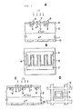
- Fig. lA shows a conventional semiconductor photoelectric transducer provided with a plurality of gates.
- Reference numeral 1 indicates an n + sillicon substrate, 2 an n layer of a low resistivity or an i layer of an intrinsic semiconductor which will ultimately serve as a channel, 3 a high impurity density first gate region reverse in conductivity type from the channel layer, 4 a high impurity density second gate region reverse in conductivity type from the channel, as is the case with the region 3, 5 a high impurity density region of the same conductivity type as the substrate 1, 7 and 10 electrodes for the substrate 1 and the high impurity density regions 5, respectively, which form a main current path of the channel, 8 a gate electrode for the second gate region 4, and 6 an insulating film layer or multilayer insulating film as of SiO 2 or Si 3 N 4 which has known insulating and surface protecting functions for isolating the electrodes 7, 8 and 9.
- Fig. 1B is a top plan view of Fig. lA. This device can be formed to have a multi-channel structure.
- Figs. lC and D show another conventional semiconductor photoelectric transducer, in which the second gate electrode 4 is provided in the form of a cross stripe. All reference numerals are the same as those used in Fig. lA.
- An object of the present invention is to provide a semiconductor photoelectric transducer which permits the separation of the functions of the first and second gates.
- Another object of the present invention is to provide a photo transistor which is arranged so that optically excited carriers are easy to store only in one of gates and the other gate is used merely as means for providing a fixed potential, thereby essentially reducing the gate capacitance to provided for improved frequency characteristics.
- a field effect transistor of static induction transistor type photoelectric transducer of the present invention which is provided with a source region and a drain region forming high impurity density main electrode regions, a high resistivity or intrinsic semiconductor region of the same conductivity type as the main electrode regions and forming a main current path therebetween, and a plurality of gate regions reverse in conductivity type from the main electrode regions and provided on both sides of the source region in the current path, for controlling a main current, and in which the distances between the gate regions and the source region are selected different from each other.
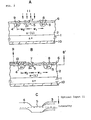
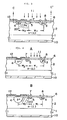
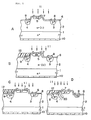
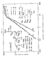
- Figs. 1A to D are diagrams explanatory of conventional semiconductor photoelectric transducers; Figs. 2A to C illustrate an embodiment of the present invention; Fig. 3 illustrates another embodiment of the present invention; Figs. 4A and B illustrate another embodiment of the present invention, in which the second gate is specially designed; Figs. 5A to D illustrate other embodiments of the present invention, in which gates are formed deeper than the source; and Fig. 6 is a graph showing the relationship between the incident light intensity and the output voltage, based on an embodiment of the present invention.
- Fig. 2A is a cross-sectional view showing the basic structure of an embodiment of the semiconductor photoelectric transducer of the present invention.
- its respective parts correspond to those, identified by the same reference numerals in Fig. 1A except that the distances W 1 and W 2 between the first and second gates 3 and 4, both having an impurity density exceeding 10 17 cm -3 , and the source 5 are not equal.
- W 1 >W 2 the light receiving area of a p + -n - (i)-n + diode between the source 5 and the gate 3 can be made larger than the light receiving area of a p + -n - (i)-n + diode between the second gate 4 and the source 5.
- the amount of change in the diffusion potential V bi of the p + -n - (i)-n + diode by the signal of the optical input 11 is such that the diffusion potential V bi (5-3) between the first gate 3 and the-source 5 varies less than does the diffusion potential V bi (5-4) between the second gate 4 and the source 5.
- the photoelectric convertion by the optical input 11 is facilitated by the voltage variations of the p + -n - (i)-n + diode between the first gate 3 and the source region 5.
- An embodiment shown in Fig. 2B is provided with a film 12 for shielding the region between the second gate 4 and the source 5 from the optical input 11.
- the light shielding film 12 need on.ly to be a metal such as, for example, aluminum or gold, resin or a film which is able to filter light of a wavelength to be applied.
- Fig. 2C shows a potential diagram, by the optical input 11 ; along the one-dot chain line B-B' in Fig. 2B.
- the optical input 11 reduces mainly the diffusion potential between the first gate 3 and the source 5, and current by the optical input 11 flows mainly between the first gate 3 and the source 5 and is difficult to occur between the second gate 4 and the source 5, so that the first gate 3 and the second gate 4 are more effective to provide the photoelectric conversion efficiency and the frequency characteristic than in the conventional semiconductor photoelectric transducers.
- Fig. 3 is a cross-sectional view illustrating another embodiment in which the impurity density of the channel is raised near the second gate 4 and the source 5 for making the diffusion potentia: V bi (5-4) between the second gate 4 and the source 5 higher than the diffusion potential V bi (5-3) between the first gate 3 and. the source 5.
- a region 20 can be formed by driving phosphorus into the channel region through the ion implantation technique.
- the diffusion potential V bi (5-3) between the first gate 3 and the source 5 becomes smaller, along the one-dot chain line in the cross-sectional view, than the diffusion potential V (5-4) between the second gate 4 and the source 5.
- Fig. 4A illustrates, in cross-section, another embodiment in which the impurity density of the second gate 4 is increased one or more orders of magnitude over the impurity density of the first gate 3 to thereby raise the diffusion potential V bi (5-4) between the second gate 4 and the source 5 higher than the diffusion potential V bi (5-3) between the first gate 3 and the source 5.
- V bi diffusion potential
- Fig. 4B is a cross-sectional view of another embodiment in which the region 20 of a higher impurity density than that of the channel is provided between the second gate 4 and the source 5 in the embodiment of Fig. 4A.
- Figs. 5A to D illustrate other embodiments in which the gate regions 3 and 4 are formed below the source region 5, decreasing the stray capacitance between each gate and the source.
- Fig. 4A shows an embodiment in which the distance between the first gate and the source is larger than the distance between the second gate and the source
- 4B an embodiment which is characterized in that the light shielding-film 12 is provided in the vicinity of the second gate in the same structure as that shown in Fig. 4A, Fig.
- Fig. 4C an embodiment which is characterized in that the impurity density of the second gate region 4 is higher than the impurity density of the first gate region 3
- Fig. 4D an embodiment which is characterized in that the impurity density of the region between the second gate and the source is further increased higher than the impurity density of the channel region in the embodiment of Fig. 4C.
- Fig. 6 shows the relationship between the incident light intensity and the optput voltage for three bit cells of 16 bits of a device provided with a 4 x 4 cell matrix structure of the Fig. 2B embodiment which is easier to fabricatie than any other embodiments of the present invention.
- the line A shows the output sensitivity to lower light intensity.
- On the first gate of each device cell is provided an internal capacitor made up of an SnO 2 /SiN/p + gate Si. Ih this trial product of the device, the second p + gate is formed in cross stripes, by simultaneous diffusion, and made equipotential throughout it.
- the device is fabricated by one high resistivity n - epitaxial growth step and two diffusion steps of a p + gate diffusion (for the first and second gates) and an n + source diffusion.
- the impurity density of the n high resistance epitaxial layer is ⁇ 10 13 cm -3 or so, and the diffusion depth of the gate is 6 to 8 p.
- the size of one cell is 100 p x 100 u , but cells of sizes up to 30 ⁇ ⁇ 3 ⁇ can easily be manufactured.
- the devices can be made small in size, and by the introduction of the structure that the gate is split into two and the sensitivity is dependent upon a specified one of them alone, the sensitivity to weak ligh is improved as compared with the sensitivity of the conventional transducers.
- a capacitor may also be provided on the first gate, and it is also possible to provide a high-speed photo sensor having connected thereto a M O S transistor or field effect transistor.
- the present invention offers a novel photo sensor in the field of the static induction transistor or FET photo sensor.
Landscapes
- Light Receiving Elements (AREA)
- Solid State Image Pick-Up Elements (AREA)
- Transforming Light Signals Into Electric Signals (AREA)
Applications Claiming Priority (2)
| Application Number | Priority Date | Filing Date | Title |
|---|---|---|---|
| JP57153429A JPS5943581A (ja) | 1982-09-03 | 1982-09-03 | 半導体光電変換装置 |
| JP153429/82 | 1982-09-03 |
Publications (3)
| Publication Number | Publication Date |
|---|---|
| EP0117874A1 true EP0117874A1 (de) | 1984-09-12 |
| EP0117874A4 EP0117874A4 (de) | 1987-01-20 |
| EP0117874B1 EP0117874B1 (de) | 1990-05-23 |
Family
ID=15562317
Family Applications (1)
| Application Number | Title | Priority Date | Filing Date |
|---|---|---|---|
| EP83902825A Expired EP0117874B1 (de) | 1982-09-03 | 1983-09-02 | Photoelektrischer umwandler mit halbleiter |
Country Status (5)
| Country | Link |
|---|---|
| US (1) | US4613881A (de) |
| EP (1) | EP0117874B1 (de) |
| JP (1) | JPS5943581A (de) |
| DE (1) | DE3381607D1 (de) |
| WO (1) | WO1984001056A1 (de) |
Cited By (1)
| Publication number | Priority date | Publication date | Assignee | Title |
|---|---|---|---|---|
| DE3344637A1 (de) * | 1982-12-11 | 1984-06-14 | Nishizawa, Jun-Ichi, Sendai, Miyagi | Photoelektrischer halbleiterwandler |
Families Citing this family (10)
| Publication number | Priority date | Publication date | Assignee | Title |
|---|---|---|---|---|
| JPS59107688A (ja) * | 1982-12-13 | 1984-06-21 | Fuji Photo Film Co Ltd | 半導体撮像装置 |
| JPS59188277A (ja) * | 1983-04-08 | 1984-10-25 | Hamamatsu Photonics Kk | 半導体撮像装置 |
| JPS60143668A (ja) * | 1983-12-29 | 1985-07-29 | Res Dev Corp Of Japan | カラ−用イメ−ジセンサ |
| JPH0828526B2 (ja) * | 1985-10-14 | 1996-03-21 | 新技術事業団 | 半導体光電変換装置の製造方法 |
| JPH0641665B2 (ja) * | 1986-06-09 | 1994-06-01 | 東レ株式会社 | 布帛の擦過処理方法および擦過処理装置 |
| US5331164A (en) * | 1991-03-19 | 1994-07-19 | California Institute Of Technology | Particle sensor array |
| US6992322B2 (en) * | 2001-01-02 | 2006-01-31 | Kavassery Sureswaran Narayan | Photo-responsive organic field effect transistor |
| WO2004070849A1 (de) * | 2003-02-06 | 2004-08-19 | Siemens Aktiengesellschaft | Sperrschicht-feldeffekttransistor |
| CN2788876Y (zh) * | 2005-05-10 | 2006-06-21 | 张逸夫 | 模拟花开动作的仿真玩具花 |
| WO2007094493A1 (ja) * | 2006-02-14 | 2007-08-23 | National Institute Of Advanced Industrial Science And Technology | 光電界効果トランジスタ、及びそれを用いた集積型フォトディテクタ |
Family Cites Families (9)
| Publication number | Priority date | Publication date | Assignee | Title |
|---|---|---|---|---|
| US3714522A (en) * | 1968-11-14 | 1973-01-30 | Kogyo Gijutsuin Agency Of Ind | Semiconductor device having surface electric-field effect |
| JPS6020910B2 (ja) * | 1977-07-07 | 1985-05-24 | 財団法人半導体研究振興会 | 静電誘導トランジスタ及び半導体集積回路 |
| US4284997A (en) * | 1977-07-07 | 1981-08-18 | Zaidan Hojin Handotai Kenkyu Shinkokai | Static induction transistor and its applied devices |
| US4326210A (en) * | 1977-09-26 | 1982-04-20 | Sharp Kabushiki Kaisha | Light-responsive field effect mode semiconductor devices |
| JPS5546548A (en) * | 1978-09-28 | 1980-04-01 | Semiconductor Res Found | Electrostatic induction integrated circuit |
| JPS56107583A (en) * | 1980-01-30 | 1981-08-26 | Matsushita Electric Ind Co Ltd | Field effect transistor |
| JPS56124273A (en) * | 1980-03-04 | 1981-09-29 | Semiconductor Res Found | Semiconductor device |
| US4422087A (en) * | 1980-06-03 | 1983-12-20 | Xerox Corporation | Self-aligned short channel MESFET |
| JPH077844B2 (ja) * | 1981-11-30 | 1995-01-30 | 財団法人半導体研究振興会 | 静電誘導型半導体光電変換装置 |
-
1982
- 1982-09-03 JP JP57153429A patent/JPS5943581A/ja active Granted
-
1983
- 1983-09-02 WO PCT/JP1983/000295 patent/WO1984001056A1/ja not_active Ceased
- 1983-09-02 US US06/610,300 patent/US4613881A/en not_active Expired - Lifetime
- 1983-09-02 EP EP83902825A patent/EP0117874B1/de not_active Expired
- 1983-09-02 DE DE8383902825T patent/DE3381607D1/de not_active Expired - Lifetime
Cited By (1)
| Publication number | Priority date | Publication date | Assignee | Title |
|---|---|---|---|---|
| DE3344637A1 (de) * | 1982-12-11 | 1984-06-14 | Nishizawa, Jun-Ichi, Sendai, Miyagi | Photoelektrischer halbleiterwandler |
Also Published As
| Publication number | Publication date |
|---|---|
| WO1984001056A1 (fr) | 1984-03-15 |
| EP0117874B1 (de) | 1990-05-23 |
| JPS6259902B2 (de) | 1987-12-14 |
| US4613881A (en) | 1986-09-23 |
| JPS5943581A (ja) | 1984-03-10 |
| DE3381607D1 (de) | 1990-06-28 |
| EP0117874A4 (de) | 1987-01-20 |
Similar Documents
| Publication | Publication Date | Title |
|---|---|---|
| EP0096725A1 (de) | Halbleiterbildaufnahmevorrichtung | |
| US4975755A (en) | Optically controllable static induction thyristor device | |
| US3858232A (en) | Information storage devices | |
| US4733286A (en) | Semiconductor photoelectric converting device | |
| US4032952A (en) | Bulk charge transfer semiconductor device | |
| EP0117874B1 (de) | Photoelektrischer umwandler mit halbleiter | |
| US3864722A (en) | Radiation sensing arrays | |
| US4651180A (en) | Semiconductor photoelectric transducer | |
| GB1602361A (en) | Semiconductor memory devices | |
| US4427990A (en) | Semiconductor photo-electric converter with insulated gate over p-n charge storage region | |
| US4686555A (en) | Solid state image sensor | |
| US5477070A (en) | Drive transistor for CCD-type image sensor | |
| JPH0454987B2 (de) | ||
| GB2172742A (en) | Photosensitive f.e.t | |
| US4641167A (en) | Semiconductor optoelectro transducer | |
| JPS5950559A (ja) | 半導体装置保護回路 | |
| EP0118568B1 (de) | Halbleiter-bildaufzeichnungsvorrichtung | |
| US4608587A (en) | Semiconductor optoelectro transducer | |
| US4494132A (en) | Semiconductor opto-electronic switch | |
| EP0038697B1 (de) | Halbleiter-Bildsensor | |
| JPS621257B2 (de) | ||
| US20020105038A1 (en) | Mos-transistor for a photo cell | |
| US5066994A (en) | Image sensor | |
| JPS59188278A (ja) | 半導体撮像装置 | |
| US5019876A (en) | Semiconductor photo-electric converter |
Legal Events
| Date | Code | Title | Description |
|---|---|---|---|
| PUAI | Public reference made under article 153(3) epc to a published international application that has entered the european phase |
Free format text: ORIGINAL CODE: 0009012 |
|
| 17P | Request for examination filed |
Effective date: 19840514 |
|
| AK | Designated contracting states |
Designated state(s): DE GB NL |
|
| A4 | Supplementary search report drawn up and despatched |
Effective date: 19870120 |
|
| 17Q | First examination report despatched |
Effective date: 19880610 |
|
| GRAA | (expected) grant |
Free format text: ORIGINAL CODE: 0009210 |
|
| AK | Designated contracting states |
Kind code of ref document: B1 Designated state(s): DE GB NL |
|
| REF | Corresponds to: |
Ref document number: 3381607 Country of ref document: DE Date of ref document: 19900628 |
|
| PLBE | No opposition filed within time limit |
Free format text: ORIGINAL CODE: 0009261 |
|
| STAA | Information on the status of an ep patent application or granted ep patent |
Free format text: STATUS: NO OPPOSITION FILED WITHIN TIME LIMIT |
|
| 26N | No opposition filed | ||
| REG | Reference to a national code |
Ref country code: GB Ref legal event code: IF02 |
|
| PGFP | Annual fee paid to national office [announced via postgrant information from national office to epo] |
Ref country code: GB Payment date: 20020828 Year of fee payment: 20 |
|
| PGFP | Annual fee paid to national office [announced via postgrant information from national office to epo] |
Ref country code: DE Payment date: 20020911 Year of fee payment: 20 |
|
| PGFP | Annual fee paid to national office [announced via postgrant information from national office to epo] |
Ref country code: NL Payment date: 20020930 Year of fee payment: 20 |
|
| PG25 | Lapsed in a contracting state [announced via postgrant information from national office to epo] |
Ref country code: GB Free format text: LAPSE BECAUSE OF EXPIRATION OF PROTECTION Effective date: 20030901 |
|
| PG25 | Lapsed in a contracting state [announced via postgrant information from national office to epo] |
Ref country code: NL Free format text: LAPSE BECAUSE OF EXPIRATION OF PROTECTION Effective date: 20030902 |
|
| REG | Reference to a national code |
Ref country code: GB Ref legal event code: PE20 |
|
| NLV7 | Nl: ceased due to reaching the maximum lifetime of a patent |
Effective date: 20030902 |