EP0120424A2 - Convertisseur analogique-numérique à comparaison parallèle - Google Patents
Convertisseur analogique-numérique à comparaison parallèle Download PDFInfo
- Publication number
- EP0120424A2 EP0120424A2 EP84102924A EP84102924A EP0120424A2 EP 0120424 A2 EP0120424 A2 EP 0120424A2 EP 84102924 A EP84102924 A EP 84102924A EP 84102924 A EP84102924 A EP 84102924A EP 0120424 A2 EP0120424 A2 EP 0120424A2
- Authority
- EP
- European Patent Office
- Prior art keywords
- circuit
- logic
- input terminal
- comparison
- gate
- Prior art date
- Legal status (The legal status is an assumption and is not a legal conclusion. Google has not performed a legal analysis and makes no representation as to the accuracy of the status listed.)
- Granted
Links
Images


Classifications
-
- H—ELECTRICITY
- H03—ELECTRONIC CIRCUITRY
- H03M—CODING; DECODING; CODE CONVERSION IN GENERAL
- H03M1/00—Analogue/digital conversion; Digital/analogue conversion
- H03M1/06—Continuously compensating for, or preventing, undesired influence of physical parameters
- H03M1/08—Continuously compensating for, or preventing, undesired influence of physical parameters of noise
- H03M1/0809—Continuously compensating for, or preventing, undesired influence of physical parameters of noise of bubble errors, i.e. irregularities in thermometer codes
-
- H—ELECTRICITY
- H03—ELECTRONIC CIRCUITRY
- H03M—CODING; DECODING; CODE CONVERSION IN GENERAL
- H03M1/00—Analogue/digital conversion; Digital/analogue conversion
- H03M1/12—Analogue/digital converters
- H03M1/34—Analogue value compared with reference values
- H03M1/36—Analogue value compared with reference values simultaneously only, i.e. parallel type
- H03M1/361—Analogue value compared with reference values simultaneously only, i.e. parallel type having a separate comparator and reference value for each quantisation level, i.e. full flash converter type
- H03M1/362—Analogue value compared with reference values simultaneously only, i.e. parallel type having a separate comparator and reference value for each quantisation level, i.e. full flash converter type the reference values being generated by a resistive voltage divider
- H03M1/365—Analogue value compared with reference values simultaneously only, i.e. parallel type having a separate comparator and reference value for each quantisation level, i.e. full flash converter type the reference values being generated by a resistive voltage divider the voltage divider being a single resistor string
Definitions
- the present invention relates to an analog to digital converter (hereinafter abbreviated as "A/D” converter) for converting an analog signal to a digital signal, and particularly to a parallel comparison type A/D converter.
- A/D analog to digital converter
- Parallel comparison type A/D converters have been widely utilized in various fields such as video systems and audio systems.
- the principle of operation of parallel comparison type A/D converters is as follows.
- An analog signal to be converted into a digital signal is simultaneously compared in a plurality of comparison circuits with a plurality of comparison voltages, respectively, each having a different value.
- the comparison circuits which receive comparison voltages of higher values than the analog signal generate output signals of a first logic level, e.g., "1", while the comparison circuits which receive comparison voltages of lower values than the analog signal generate output signals of a second logic level e.g., "0".
- the output signals are applied to a corresponding plurality of logic gates in such a manner that the logic gates determine which comparison voltage is closest to the analog signal.
- An output of only one of the logic gates is activated, e.g., binary "I", while outputs of the remaining logic gates are not activated.
- the particular logic gate having the activated output corresponds to the value of the analog signal.
- the outputs of the logic gates are applied to a decoder and a binary code representing the value of the analog signal.
- the disadvantage described above is fatal to the A/ D converters. Namely, when the A/D converter is used to convert an analog signal such as an audio or video signal, which changes continuously in value, an output digital signal becomes noisy.
- One possible way to overcome the above disadvantage is to increase the sensitivity of the comparison circuits so that the outputs will never have an intermediate value.
- the number of the comparators used in parallel comparison type A/D converters is very large (for example, 2 N comparators are required for an A/D converter of an N-bit output structure), and a large number of circuit elements such as field effect tran- ' sistors is required to obtain high sensitivity. Therefore, it has been difficult and impractical to form;a parallel comparison type A/D converter having very highly sensitive comparators on a limited area of a semiconductor chip.
- a parallel comparison type A/D converter comprises an ordered plurality of comparators, each having different weight and comparing an analog signal with a comparison voltage corresponding to its weight, and a plurality of logic gates for determining the closest weight to the analog signal, each of the logic gates having a first input terminal of a positive logic and a second input terminal of a negative logic, the first input terminal receiving an output signal from one of the comparators having a certain weight, and the second input terminal receiving an output signal from the comparator having the subsequent weight to the certain weight, and is featured that threshold values of the first and second input terminals are made different from each other.
- the comparator if the comparator generates an output signal of an intermediate value which is not classified into either of two binary logic levels, such an output signal of the intermediate level is necessarily recognized as one of the binary logic signals by at least one of the first and second input terminals.
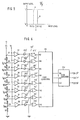
- an analog signal is converted into a 3-bit digital or binary signal.
- a voltage dividing circuit 10 is connected between a reference voltage V R and a ground potential GND.
- the voltage dividing circuit 10 consists of a plurality of resistors 12 to 19, in which a plurality of divided voltages are derived from nodes 20 to 27 between the respective resistors.
- the output nodes 20 to 27 of the voltage dividing circuit 10 are connected to inverted input terminals (-) of a plurality of comparators 30 to 37, respectively.
- An analog signal V s is applied in common to uninverted terminals (+) of the comparators.
- a position detecting logical circuit 50 consists of a plurality of logic gates 40 to 47, and the outputs of this circuit 50 are connected to a first code converter 151.
- the outputs of the first code converter 151 are applied to a second code converter 251 generating a 3-bit digital output 252 to 254.
- the voltage divider provides a plurality of comparison voltages, with the lowest voltage being at node 20, the next highest at node 21, etc., through the highest at node 27.
- the comparison voltages will be referred to herein as an ordered plurality of comparison voltages for the purpose of describing the relationships between the comparison voltages, a like ordered plurality of comparison circuits 30-37, and a like ordered plurality of logic circuits.
- each comparison circuit receives the comparison voltage, e.g., at node 23, of the same order.
- Each logic gate, e.g., 43 receives one input at a positive logic terminal from the comparison circuit of the same order, e.g., 33, receives a second input at a negative logic input terminal from the comparison circuit which precedes it by one in the order, e.g., 32, and receives a third input at a positive logic input terminal from the comparison circuit which succeeds it by one in the order, e.g., 34.
- the elements may be described as having weights, even though all the comparison circuits and all the logic circuits may be identical.
- the gate 43 has a weight which is one above that of gate 42 and corresponds to the weight of comparison circuit 33 and the comparison voltage at node 33.
- first binary level signal e.g., "0”
- second binary level signal e.g., "1"
- Logic gate 44 will be the only gate activated and will thus be the only logic gate providing a binary "1" level output to the code converter 151.
- the “order of the crossover” refers to the position of the change from “0" outputs to “1" outputs from the plurality of comparison circuits.
- the outputs from the positiondetecting logical circuit 50 are decoded in the first code converter 151 ta obtain 3-bit digital signals.
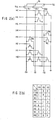
- the first code converter 151 may consist of a read-only memory (ROM) shown in Figure 2a, the codes of which produce a binary Gray code output as shown in tabular form in Figure 2b.
- the Gray code is converted into a regular binary code by the second code converter 251 to obtain an analog-digital converted. output corresponding to the analog input voltage V S .
- the second code converter 251, which is adapted to convert Gray code into the binary code may consist of exclusive OR gates EXGl and EXG2 as shown in Figure 3.
- the Gray code converter 151 has the disadvantage that when the outputs of the gates 40 to 47 are all "0" level, a certain special code is output therefrom. As illustrated that code is 111, the same as would occur if logic gate 145 provided a binary "1" at its output.
- both gates 43 and 44 will have the same recognition of the X level signal. That is, both will recognize the X level signal as a "0" if below the binary threshold level; both will recognize the X level signal as a "1” if above the binary threshold level. In either case, one and only one of gates 43 and 44 will output a binary 1 to the Gray code converter.
- the binary threshold levels of all inputs are not always equal to one another. If the input threshold value V T 43 at a positive logic input terminal (without circle 0) of the gate 43 is higher than V T 44 of a negative logic input terminal (with circle 0) of the gate 44 due to the deviation of manufacturing accuracy, the same input level "X" from the comparator 33 is recognized as "0" level with respect to the positive logic input terminal of the gate 43, and as "1" level with respect to the negative logic input terminal of the gate 44. Consequently, the levels of outputs from the gates 43 and 44 become “0", and none of the input terminals 40 to 47 of the Gray code converter is selected. When no input terminals of the first code converter 151 is selected, a code 111 appears at the outputs 152 to 154. Accordingly, "101" necessarily appears at the outputs of the second code converter 251.
- a voltage dividing circuit 10 composed of 2N resistors 12 to 19 is connected between a reference voltage V R and a ground potential GND.
- An ordered plurality of comparators 30 to 37 receive the ordered plurality of comparison voltages from nodes 20 to 27 at their inverted input terminals (-), respectively, and an analog signal V at their uninverted input terminals (+) in common.
- a position detecting logic circuit 50' includes an ordered plurality of gating circuits, each consisting of an AND gate and an inverter gate; the AND gates 401-471 constituting a first logic circuit means, and the inverter gates 402-473 constituting a second logic circuit means. The function of position detecting circuit 50' is to detect a digitized location of the analog signal V S similarly to the circuit 50 in Figure 1.
- the logic of the converter of Figure 4 is the same as that of Figure 1.
- each logic gate of Figure 1 into an AND gate and an inverter gate, the problem described above can be easily avoided.
- the AND gates 401-471 are fabricated to have a first binary threshold level at a relatively low value
- the inverter gates are fabricated to have a second binary threshold level at a relatively high value.
- the third possibility is that the level X will be intermediate the threshold VT431 of AND gate 431 and threshold V T442 of invert gate 442.
- AND gate 431 will recognize the level X signal as a "1” and will output a binary "1”; invert gate 442 will recognize the level X as a "0” and will cause AND gate 441 to output a binary "1".
- the intermediate level result in all "0's" being output from position detection circuit 50'.
- One example of suitable voltages for the circuit described is as follows.
- the output of each of the comparators 30 to 37 swings between OV as a logic "0" level and 5V as a logic "1" level. Therefore, the intermediate value "X" of the output of the comparator is about 2.5V.
- the threshold value V T431 of the AND gates 4 01-471 is about 2V.
- the threshold value V T442 of the inverter gates 402-472 is about 3V.
- a certain output code is converted normally into a subsequent output code even when an output from a comparator has any degree of intermediate level "X"; no abnormal code is outputted.
- a position detecting circuit 50" comprises a first logic circuit consisting of invert gates 402'-472' and a second logic circuit consisting of NOR gates 401'-471'. It will be appreciated that the converter of Figure 6 differs from that of Figure 4 only in that the circuitry of position detector 50" is the inverse logic equivalent of the circuitry of position detector 50'.
- detector 50' Figure 4
- an AND gate (431) receives direct inputs from the comparison circuit (33) of the same order, and from the comparison circuit (34) which succeeds it by one in the order, and receives an inverted input from the comparison circuit (32) which precedes it by one in the order
- NOR gate (431') receives inverted inputs from the comparison circuit (33) of the same order and from the comparison circuit (34) which succeeds it by one in the order, and receives a direct input from the comparison circuit (32) which precedes it by one in the order.
- An input threshold value of logic input gates 401', 411', 421', 431', 441', 451', 461' and 471' is set relatively higher than that of the inverters 402', 412', 432', 442', 452', 462' and 472', thereby to intentionally make these two threshold values different, so that, when an output from a comparator has an intermediate level, an output from the position-detecting logic circuit 50" can be doubly selected by a first code converter 151.
- a method of adjusting the threshold value of a logic gate to a desired value is not limited. Many known methods for adjusting the threshold value of logic circuits are applicable to achieve the present invention. A typical method will be explained below.
- An input threshold value V T for a logic gate can generally be varied with a combination of a gate length (L) and a gate width (W) of a MOS transistor, which constitutes the logic gate.
- L L and W L be the gate length and a gate width, respectively, of a transistor operating as a load
- L D and W D be the gate length and a gate width, respectively, of a transistor operating as a driver.
- an effective input threshold value V Teff for the logic gate can be expressed by the following formula.
- a parallel comparison type A/D converter is free from the occurrence of abnormal code outputs, which is due to an insecure output from a comparator, and, therefore, it can maintain its monotonic operation.
- comparators of a higher accuracy need not be employed for the purpose of preventing the occurrence of insecure outputs therefrom, and a large-scale complicated circuit need not be employed, either, for the purpose of enabling the comparators to have higher gain.
- no other special circuits and no special manufacturing steps are required. Accordingly, the present invention can provide a reliable parallel comparison type A/D converter capable of easily forming a monolithic integrated circuit of a comparatively simple construction.
Landscapes
- Engineering & Computer Science (AREA)
- Theoretical Computer Science (AREA)
- Analogue/Digital Conversion (AREA)
Applications Claiming Priority (2)
| Application Number | Priority Date | Filing Date | Title |
|---|---|---|---|
| JP58045471A JPS59171315A (ja) | 1983-03-18 | 1983-03-18 | アナログ−デジタル変換器 |
| JP45471/83 | 1983-03-18 |
Publications (3)
| Publication Number | Publication Date |
|---|---|
| EP0120424A2 true EP0120424A2 (fr) | 1984-10-03 |
| EP0120424A3 EP0120424A3 (en) | 1988-12-14 |
| EP0120424B1 EP0120424B1 (fr) | 1992-06-03 |
Family
ID=12720299
Family Applications (1)
| Application Number | Title | Priority Date | Filing Date |
|---|---|---|---|
| EP84102924A Expired EP0120424B1 (fr) | 1983-03-18 | 1984-03-16 | Convertisseur analogique-numérique à comparaison parallèle |
Country Status (4)
| Country | Link |
|---|---|
| US (1) | US4596978A (fr) |
| EP (1) | EP0120424B1 (fr) |
| JP (1) | JPS59171315A (fr) |
| DE (1) | DE3485753T2 (fr) |
Cited By (5)
| Publication number | Priority date | Publication date | Assignee | Title |
|---|---|---|---|---|
| US4737766A (en) * | 1986-09-12 | 1988-04-12 | North American Philips Corporation, Signetics Division | Code converter with complementary output voltages |
| EP0282147A3 (fr) * | 1987-02-09 | 1990-04-11 | Tektronix Inc. | Circuit de correction d'erreur de convertisseur analogique-numérique |
| EP0282154A3 (fr) * | 1987-03-09 | 1990-09-12 | Tektronix Inc. | Convertisseur analogique-numérique avec circuits de vérification et de correction d'erreur |
| WO1991012669A1 (fr) * | 1990-02-15 | 1991-08-22 | Siemens Aktiengesellschaft | Circuit de codage |
| EP0436555A4 (en) * | 1988-08-04 | 1993-01-27 | Signal Processing Technologies, Inc. | Error limiting analog to digital converter |
Families Citing this family (20)
| Publication number | Priority date | Publication date | Assignee | Title |
|---|---|---|---|---|
| US4954831A (en) * | 1986-06-18 | 1990-09-04 | Ekins Robin K | Analog-to-digital converter |
| US4860011A (en) * | 1986-10-27 | 1989-08-22 | Brooktree Corporation | Flash analog-to-digital converter |
| US4745394A (en) * | 1987-04-03 | 1988-05-17 | Motorola, Inc. | Pipelined A/D converter |
| US4963874A (en) * | 1987-04-28 | 1990-10-16 | Matsushita Electric Industrial Co., Ltd. | Parallel type A/D converter |
| FR2623668B1 (fr) * | 1987-11-20 | 1990-03-09 | Thomson Composants Militaires | Convertisseur analogique-numerique rapide a structure parallele |
| US4884075A (en) * | 1988-05-19 | 1989-11-28 | Analog Devices, Inc. | Decoding circuit for flash-type analog-to-digital converter |
| FR2638037B1 (fr) * | 1988-10-14 | 1994-04-08 | Thomson Hybrides Microondes | Convertisseur analogique-numerique parallele, a circuit de correction d'erreur |
| US4965579A (en) * | 1988-11-28 | 1990-10-23 | The Board Of Governors Of Wayne State University | N-bit A/D converter utilizing N comparators |
| US5119098A (en) * | 1989-06-20 | 1992-06-02 | Sony Corporation | Full flash analog-to-digital converter |
| US4928103A (en) * | 1989-09-18 | 1990-05-22 | Analog Devices, Inc. | Parallel analog-to-digital converter using 2.sup.(n-1) comparators |
| US4975698A (en) * | 1989-12-08 | 1990-12-04 | Trw Inc. | Modified quasi-gray digital encoding technique |
| JP3229135B2 (ja) * | 1994-09-14 | 2001-11-12 | 三菱電機株式会社 | アナログ/デジタル変換装置 |
| KR100703885B1 (ko) * | 2005-07-18 | 2007-04-06 | 삼성전자주식회사 | 외부 공급 전압으로부터 적응적으로 내부 전압을 발생하는장치 및 그 방법 |
| JP4407747B2 (ja) * | 2007-12-13 | 2010-02-03 | ソニー株式会社 | A/d変換器及び情報記録再生装置 |
| US7893855B2 (en) * | 2008-09-16 | 2011-02-22 | Mediatek Inc. | Delta-sigma analog-to-digital converter |
| JP4777444B2 (ja) * | 2009-03-03 | 2011-09-21 | シャープ株式会社 | デコーダ装置および移動制御装置 |
| CN112751561A (zh) * | 2019-10-31 | 2021-05-04 | 中车株洲电力机车研究所有限公司 | 单通道输入多状态输出电路和方法、车辆 |
| CN111431523A (zh) * | 2020-04-15 | 2020-07-17 | 联合华芯电子有限公司 | 多进制符号逻辑异或运算的实现电路、装置及方法 |
| CN111371448A (zh) * | 2020-04-15 | 2020-07-03 | 联合华芯电子有限公司 | 一种实现多电平逻辑异或、比同运算的电路和方法 |
| CN111327310A (zh) * | 2020-04-15 | 2020-06-23 | 联合华芯电子有限公司 | 一种实现多电平逻辑或运算的电路和方法 |
Family Cites Families (8)
| Publication number | Priority date | Publication date | Assignee | Title |
|---|---|---|---|---|
| JPS4957759A (fr) * | 1972-10-02 | 1974-06-05 | ||
| FR2222800A1 (en) * | 1973-03-23 | 1974-10-18 | Thomson Csf | High performance analogue-digital converter - comprising integrated circuit modules of comparators and nor circuits |
| JPS5441061A (en) * | 1977-09-08 | 1979-03-31 | Sony Corp | Analogue/digital converter |
| US4251802A (en) * | 1977-12-28 | 1981-02-17 | Horna Otakar A | Analog to digital converter |
| JPS5658323A (en) * | 1979-10-18 | 1981-05-21 | Matsushita Electric Ind Co Ltd | Analog-digital converter |
| JPS57204633A (en) * | 1981-06-10 | 1982-12-15 | Toshiba Corp | Analog-to-digital converter |
| JPS58142622A (ja) * | 1982-02-18 | 1983-08-24 | Nec Corp | アナログ・デジタル変換器 |
| US4393372A (en) * | 1982-03-08 | 1983-07-12 | Itt Industries, Inc. | Parallel analog-to-digital converter |
-
1983
- 1983-03-18 JP JP58045471A patent/JPS59171315A/ja active Granted
-
1984
- 1984-03-16 EP EP84102924A patent/EP0120424B1/fr not_active Expired
- 1984-03-16 DE DE8484102924T patent/DE3485753T2/de not_active Expired - Lifetime
- 1984-03-19 US US06/590,618 patent/US4596978A/en not_active Expired - Lifetime
Cited By (6)
| Publication number | Priority date | Publication date | Assignee | Title |
|---|---|---|---|---|
| US4737766A (en) * | 1986-09-12 | 1988-04-12 | North American Philips Corporation, Signetics Division | Code converter with complementary output voltages |
| EP0282147A3 (fr) * | 1987-02-09 | 1990-04-11 | Tektronix Inc. | Circuit de correction d'erreur de convertisseur analogique-numérique |
| EP0282154A3 (fr) * | 1987-03-09 | 1990-09-12 | Tektronix Inc. | Convertisseur analogique-numérique avec circuits de vérification et de correction d'erreur |
| EP0436555A4 (en) * | 1988-08-04 | 1993-01-27 | Signal Processing Technologies, Inc. | Error limiting analog to digital converter |
| WO1991012669A1 (fr) * | 1990-02-15 | 1991-08-22 | Siemens Aktiengesellschaft | Circuit de codage |
| US5272461A (en) * | 1990-02-15 | 1993-12-21 | Siemens Aktiengesellschaft | Coding circuit |
Also Published As
| Publication number | Publication date |
|---|---|
| JPH0125449B2 (fr) | 1989-05-17 |
| EP0120424B1 (fr) | 1992-06-03 |
| DE3485753T2 (de) | 1992-12-24 |
| EP0120424A3 (en) | 1988-12-14 |
| US4596978A (en) | 1986-06-24 |
| JPS59171315A (ja) | 1984-09-27 |
| DE3485753D1 (de) | 1992-07-09 |
Similar Documents
| Publication | Publication Date | Title |
|---|---|---|
| US4596978A (en) | Parallel comparison type analog to digital converter | |
| US5072221A (en) | Error limiting analog to digital converter | |
| US4644322A (en) | Analog-to-digital converter | |
| JP2800233B2 (ja) | Ad変換器 | |
| US5194867A (en) | Flash analog-to-digital converter employing least significant bit-representative comparative reference voltage | |
| US6346905B1 (en) | Analog-to-digital flash converter for generating a thermometric digital code | |
| US6034671A (en) | Photocoupling signal detection circuit for a computer mouse | |
| US5623265A (en) | Flash analog-to-digital converter and method of operation | |
| JP2007143185A (ja) | アナログ信号をデジタル信号に変換するアナログデジタル変換器および方法 | |
| US20040108949A1 (en) | Bubble handling a/d converter calibration | |
| US4999630A (en) | Fast analog-digital converter with parallel structure | |
| US6417700B1 (en) | Voltage level detection circuit and voltage level detection method | |
| JPH0997839A (ja) | 機能選択が可能な集積回路およびその機能選択方法 | |
| EP0328213A2 (fr) | Circuit de synchronisation de transitions de bits d'un code numérique | |
| US4918451A (en) | A/D converter with prevention of comparator output discontinuities | |
| US4692640A (en) | Majority circuit comprising binary counter | |
| US5361289A (en) | Synchronous counter circuit having a plurality of cascade-connected counters | |
| EP0259936B1 (fr) | Convertisseur de code à tensions de sortie complémentaires | |
| JPS63232526A (ja) | Ad変換器 | |
| US5307061A (en) | Absolute value circuit | |
| JPH10209823A (ja) | ヒステリシスコンパレータ | |
| JPH0681050B2 (ja) | 並列形ad変換器 | |
| JPH0787371B2 (ja) | 並列型a/d変換器 | |
| JPH0429258B2 (fr) | ||
| JPS6282823A (ja) | 符号変換回路 |
Legal Events
| Date | Code | Title | Description |
|---|---|---|---|
| PUAI | Public reference made under article 153(3) epc to a published international application that has entered the european phase |
Free format text: ORIGINAL CODE: 0009012 |
|
| 17P | Request for examination filed |
Effective date: 19840710 |
|
| AK | Designated contracting states |
Designated state(s): DE FR GB NL |
|
| PUAL | Search report despatched |
Free format text: ORIGINAL CODE: 0009013 |
|
| AK | Designated contracting states |
Kind code of ref document: A3 Designated state(s): DE FR GB NL |
|
| 17Q | First examination report despatched |
Effective date: 19900704 |
|
| GRAA | (expected) grant |
Free format text: ORIGINAL CODE: 0009210 |
|
| AK | Designated contracting states |
Kind code of ref document: B1 Designated state(s): DE FR GB NL |
|
| REF | Corresponds to: |
Ref document number: 3485753 Country of ref document: DE Date of ref document: 19920709 |
|
| ET | Fr: translation filed | ||
| PLBE | No opposition filed within time limit |
Free format text: ORIGINAL CODE: 0009261 |
|
| STAA | Information on the status of an ep patent application or granted ep patent |
Free format text: STATUS: NO OPPOSITION FILED WITHIN TIME LIMIT |
|
| 26N | No opposition filed | ||
| REG | Reference to a national code |
Ref country code: GB Ref legal event code: IF02 |
|
| PGFP | Annual fee paid to national office [announced via postgrant information from national office to epo] |
Ref country code: FR Payment date: 20030310 Year of fee payment: 20 |
|
| PGFP | Annual fee paid to national office [announced via postgrant information from national office to epo] |
Ref country code: GB Payment date: 20030312 Year of fee payment: 20 |
|
| PGFP | Annual fee paid to national office [announced via postgrant information from national office to epo] |
Ref country code: NL Payment date: 20030327 Year of fee payment: 20 Ref country code: DE Payment date: 20030327 Year of fee payment: 20 |
|
| REG | Reference to a national code |
Ref country code: GB Ref legal event code: 732E |
|
| NLS | Nl: assignments of ep-patents |
Owner name: NEC ELECTRONICS CORPORATION |
|
| REG | Reference to a national code |
Ref country code: FR Ref legal event code: TP |
|
| PG25 | Lapsed in a contracting state [announced via postgrant information from national office to epo] |
Ref country code: GB Free format text: LAPSE BECAUSE OF EXPIRATION OF PROTECTION Effective date: 20040315 |
|
| PG25 | Lapsed in a contracting state [announced via postgrant information from national office to epo] |
Ref country code: NL Free format text: LAPSE BECAUSE OF EXPIRATION OF PROTECTION Effective date: 20040316 |
|
| REG | Reference to a national code |
Ref country code: GB Ref legal event code: PE20 |
|
| NLV7 | Nl: ceased due to reaching the maximum lifetime of a patent |
Effective date: 20040316 |