EP0124075A1 - Dispositif de support pour cible à pulvériser - Google Patents
Dispositif de support pour cible à pulvériser Download PDFInfo
- Publication number
- EP0124075A1 EP0124075A1 EP84104644A EP84104644A EP0124075A1 EP 0124075 A1 EP0124075 A1 EP 0124075A1 EP 84104644 A EP84104644 A EP 84104644A EP 84104644 A EP84104644 A EP 84104644A EP 0124075 A1 EP0124075 A1 EP 0124075A1
- Authority
- EP
- European Patent Office
- Prior art keywords
- electrode
- beams
- holder
- supporting device
- shaped
- Prior art date
- Legal status (The legal status is an assumption and is not a legal conclusion. Google has not performed a legal analysis and makes no representation as to the accuracy of the status listed.)
- Granted
Links
- 238000005477 sputtering target Methods 0.000 title claims abstract description 6
- 238000003825 pressing Methods 0.000 claims abstract description 11
- 238000004544 sputter deposition Methods 0.000 claims abstract description 11
- 230000007246 mechanism Effects 0.000 claims abstract description 9
- 230000002093 peripheral effect Effects 0.000 claims description 3
- ZOKXTWBITQBERF-UHFFFAOYSA-N Molybdenum Chemical compound [Mo] ZOKXTWBITQBERF-UHFFFAOYSA-N 0.000 description 5
- XUIMIQQOPSSXEZ-UHFFFAOYSA-N Silicon Chemical compound [Si] XUIMIQQOPSSXEZ-UHFFFAOYSA-N 0.000 description 5
- 239000000203 mixture Substances 0.000 description 5
- 229910052750 molybdenum Inorganic materials 0.000 description 5
- 239000011733 molybdenum Substances 0.000 description 5
- 229910052710 silicon Inorganic materials 0.000 description 5
- 239000010703 silicon Substances 0.000 description 5
- 238000001816 cooling Methods 0.000 description 4
- 239000010409 thin film Substances 0.000 description 4
- 230000003247 decreasing effect Effects 0.000 description 3
- 239000010408 film Substances 0.000 description 2
- 229910020968 MoSi2 Inorganic materials 0.000 description 1
- 239000000956 alloy Substances 0.000 description 1
- 229910045601 alloy Inorganic materials 0.000 description 1
- 238000000151 deposition Methods 0.000 description 1
- 229910052751 metal Inorganic materials 0.000 description 1
- 239000002184 metal Substances 0.000 description 1
- 238000000034 method Methods 0.000 description 1
- 230000000717 retained effect Effects 0.000 description 1
Images

Classifications
-
- H—ELECTRICITY
- H01—ELECTRIC ELEMENTS
- H01J—ELECTRIC DISCHARGE TUBES OR DISCHARGE LAMPS
- H01J37/00—Discharge tubes with provision for introducing objects or material to be exposed to the discharge, e.g. for the purpose of examination or processing thereof
- H01J37/32—Gas-filled discharge tubes
- H01J37/34—Gas-filled discharge tubes operating with cathodic sputtering
- H01J37/3411—Constructional aspects of the reactor
- H01J37/3414—Targets
- H01J37/3423—Shape
-
- C—CHEMISTRY; METALLURGY
- C23—COATING METALLIC MATERIAL; COATING MATERIAL WITH METALLIC MATERIAL; CHEMICAL SURFACE TREATMENT; DIFFUSION TREATMENT OF METALLIC MATERIAL; COATING BY VACUUM EVAPORATION, BY SPUTTERING, BY ION IMPLANTATION OR BY CHEMICAL VAPOUR DEPOSITION, IN GENERAL; INHIBITING CORROSION OF METALLIC MATERIAL OR INCRUSTATION IN GENERAL
- C23C—COATING METALLIC MATERIAL; COATING MATERIAL WITH METALLIC MATERIAL; SURFACE TREATMENT OF METALLIC MATERIAL BY DIFFUSION INTO THE SURFACE, BY CHEMICAL CONVERSION OR SUBSTITUTION; COATING BY VACUUM EVAPORATION, BY SPUTTERING, BY ION IMPLANTATION OR BY CHEMICAL VAPOUR DEPOSITION, IN GENERAL
- C23C14/00—Coating by vacuum evaporation, by sputtering or by ion implantation of the coating forming material
- C23C14/22—Coating by vacuum evaporation, by sputtering or by ion implantation of the coating forming material characterised by the process of coating
- C23C14/34—Sputtering
- C23C14/3407—Cathode assembly for sputtering apparatus, e.g. Target
-
- H—ELECTRICITY
- H01—ELECTRIC ELEMENTS
- H01J—ELECTRIC DISCHARGE TUBES OR DISCHARGE LAMPS
- H01J37/00—Discharge tubes with provision for introducing objects or material to be exposed to the discharge, e.g. for the purpose of examination or processing thereof
- H01J37/32—Gas-filled discharge tubes
- H01J37/34—Gas-filled discharge tubes operating with cathodic sputtering
-
- H—ELECTRICITY
- H01—ELECTRIC ELEMENTS
- H01J—ELECTRIC DISCHARGE TUBES OR DISCHARGE LAMPS
- H01J37/00—Discharge tubes with provision for introducing objects or material to be exposed to the discharge, e.g. for the purpose of examination or processing thereof
- H01J37/32—Gas-filled discharge tubes
- H01J37/34—Gas-filled discharge tubes operating with cathodic sputtering
- H01J37/3411—Constructional aspects of the reactor
- H01J37/3414—Targets
- H01J37/3426—Material
- H01J37/3429—Plural materials
Definitions
- the present invention relates to a sputtering target supporting device, and particularly to a device- for securing, to a common electrode, a plurality of beams forming a mosaic target used for co-sputtering two or more kinds of metal to form a thin film.
- a mosaic target comprising, in combination, molybdenum beams 1 and silicon beams 2 as shown in Fig. 1 is used.
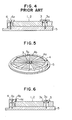
- Beams 1 and 2 are fixed to an electrode 5, which also serves as a radiator or cooling plate, by having an inner holder 3 and an annular outer holder 4, shown in F ig. 2, secured to the electrode 5 by means of screws 3a and 4a, as shown in Figs. 3 and 4.
- the above-described fixing method has a disadvantage in that contact pressure between the beam and the electrode is not sufficient with respect to some of the beams because of an error in the dimensions of the beams and the holders.
- the contact pressure is insufficient, the contact resistance is increased.
- the electrode 5 also serves as a cooling plate as described above, so that the decreased contact pressure makes the cooling of the beam insufficient. For this reason, the temperature of the beam increases, and an electric power used for the discharge becomes insufficient.
- sputtering yield is decreased.
- the sputtering yield of some of the beams may be so much decreased that it is smaller than the rate of re-deposition of the ionized sputter atoms. Consequently, the composition of the thin film formed by sputtering varies.
- An object of the invention is to provide a sputtering target supporting device which is capable of preventing decrease of sputtering yield of each beam, and of maintaining constant the composition of_the thin film formed by co-sputtering.
- a sputtering target supporting device for fixing, to a common electrode,'a plurality of beams forming a mosaic target used for co-sputtering, wherein at least one pressing mechanism is provided exclusively for each of the beams to press the respective beam against the common electrode by means of said at least one pressing mechanism provided therefor.
- Figs. 5 and 6 show a supporting device of an embodiment of the invention.
- This supporting device is, as is the supporting device of Fig. 1, for securing molybdenum beams 1 and silicon beams 2, which are wedge-shaped and so arranged that they, as a whole, form an annulus, and mounted or placed on a substantially disk-shaped electrode 5.
- the beams are held or retained, at their inner or narrower ends, by an inner- holder 3. And, at their outer or wider ends, by an outer holder 4.
- the outer holder 4 extends along the outer periphery of the disk-shaped electrode, and fixed: to the outer peripheral portion by means of screws 4a, and is used to press, in a manner described later, the wider end of each of the wedge-shaped beams against the outer peripheral portion of the electrode 5.
- the inner holder 3 is positioned at the center of the disk-shaped electrode 5, and is fixed to the central portion of the electrode 5 by means of a screw 3a, to press, by an overhang 3c extending toward the outer periphery of the electrode 5, the narrower end of each of the wedge-shaped beams against the central portion of the electrode.
- the outer holder 4 has an overhang 4c extending toward the central portion of the electrode 5, and the wider ends of the beams 1 and 2 are inserted between the overhang 4c and the electrode 5.
- a plurality of screws 4b are threaded in the overhang 4c of the outer holder 4. As shown in Fig. 5, at least one such screw 4b is provided for each beam. In the illustrated example, one screw 4b is provided for each of relatively narrow molybdenum beam, whereas two screws 4b are provided for each of relatively wide silicon beams. Ends of the screws 4b are, as shown in Fig. 6, in abutment with the upper surfaces of the beams and press the respective beams down, i.e., against the electrode 5.
- At least one screw 4b is provided exclusively for each beam, and serves to press each beam individually against the electrode 5, so that the contact pressure between the beam and the electrode is sufficient with respect to each of the beams.
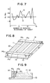
- the ratio Si/Mo of the composition varies substantially, as shown by a curve A, every time the target is re-assembled.
- the ratio is maintained (at 2.0, for example) as shown by a curve B.
- the mosaic target is an assembly of wedge-shaped beams 1 and 2 and is generally annular or disk-shaped.
- the invention is not limited to such specific shape of the mosaic target, and is applicable to a situation where, as shown in Figs. 8 and 9, strip-shaped beams are placed side by side and their both ends are fixed by means of a pair of holders 14.
- at least one screw 14b is provided for each end of each beam.
- Each screw 14b is threaded in a overhang 14c of the holder 14 and abuts, at its end, an end of the beam, to press the beam against the electrode 15.
- a larger member (two, in the illustrated example) of screws 14b may be provided for relatively wide beams.
- screws 4b or 14b are used as mechanisms for pressing. But it will be understood that any other device having the same function can be used as an alternative.
- An example is a spring mounted to the holder and adopted to press each beam against the electrode.
Landscapes
- Chemical & Material Sciences (AREA)
- Engineering & Computer Science (AREA)
- Physics & Mathematics (AREA)
- Analytical Chemistry (AREA)
- Plasma & Fusion (AREA)
- Materials Engineering (AREA)
- Organic Chemistry (AREA)
- Metallurgy (AREA)
- Mechanical Engineering (AREA)
- Chemical Kinetics & Catalysis (AREA)
- Physical Vapour Deposition (AREA)
- Electrodes Of Semiconductors (AREA)
- Physical Deposition Of Substances That Are Components Of Semiconductor Devices (AREA)
Applications Claiming Priority (2)
| Application Number | Priority Date | Filing Date | Title |
|---|---|---|---|
| JP75098/83 | 1983-04-28 | ||
| JP58075098A JPS59200761A (ja) | 1983-04-28 | 1983-04-28 | スパツタリングタ−ゲツト支持装置 |
Publications (2)
| Publication Number | Publication Date |
|---|---|
| EP0124075A1 true EP0124075A1 (fr) | 1984-11-07 |
| EP0124075B1 EP0124075B1 (fr) | 1986-12-17 |
Family
ID=13566352
Family Applications (1)
| Application Number | Title | Priority Date | Filing Date |
|---|---|---|---|
| EP84104644A Expired EP0124075B1 (fr) | 1983-04-28 | 1984-04-25 | Dispositif de support pour cible à pulvériser |
Country Status (4)
| Country | Link |
|---|---|
| US (1) | US4485000A (fr) |
| EP (1) | EP0124075B1 (fr) |
| JP (1) | JPS59200761A (fr) |
| DE (1) | DE3461722D1 (fr) |
Cited By (7)
| Publication number | Priority date | Publication date | Assignee | Title |
|---|---|---|---|---|
| GB2173217A (en) * | 1985-04-03 | 1986-10-08 | Balzers Hochvakuum | Target holder for cathodic sputtering |
| EP0281141A1 (fr) * | 1987-03-06 | 1988-09-07 | Kabushiki Kaisha Toshiba | Cible de pulvérisation |
| GB2228948A (en) * | 1989-02-28 | 1990-09-12 | British Aerospace | Fabrication of thin films from a composite target |
| EP0413354A1 (fr) * | 1989-08-17 | 1991-02-20 | Mitsubishi Kasei Corporation | Cible de pulvÀ©risation pour pulvérisation réactive cathodique à magnétron, procédé de formation d'une couche mince pour utilisation d'une telle cible, et disque optique présentant une couche formée par ce procédé |
| EP0826229B1 (fr) * | 1995-05-19 | 2003-02-19 | Lam Research Corporation | Dispositif de serrage pour une electrode, son assemblage et son utilisation |
| EP2434523A3 (fr) * | 2010-09-28 | 2014-04-30 | First Solar Malaysia SDN.BHD | Cathode de pulvérisation dotée d'une cible semi-conductrice non liée |
| EP2434524A3 (fr) * | 2010-09-28 | 2014-09-10 | First Solar Malaysia SDN.BHD | Procédés de pulvérisation utilisant une cible semi-conductrice non liée |
Families Citing this family (25)
| Publication number | Priority date | Publication date | Assignee | Title |
|---|---|---|---|---|
| US4634512A (en) * | 1984-08-21 | 1987-01-06 | Komag, Inc. | Disk and plug |
| US4834855A (en) * | 1985-05-02 | 1989-05-30 | Hewlett-Packard Company | Method for sputter depositing thin films |
| US4626336A (en) * | 1985-05-02 | 1986-12-02 | Hewlett Packard Company | Target for sputter depositing thin films |
| US4793975A (en) * | 1985-05-20 | 1988-12-27 | Tegal Corporation | Plasma Reactor with removable insert |
| CH669242A5 (de) * | 1985-07-10 | 1989-02-28 | Balzers Hochvakuum | Targetplatte fuer kathodenzerstaeubung. |
| JPS62116761A (ja) * | 1985-11-15 | 1987-05-28 | Sanyo Electric Co Ltd | マスキング装置 |
| DE3613018A1 (de) * | 1986-04-17 | 1987-10-22 | Santos Pereira Ribeiro Car Dos | Magnetron-zerstaeubungskathode |
| DE3912381A1 (de) * | 1988-04-15 | 1989-10-26 | Sharp Kk | Auffaengereinheit |
| JPH0387358A (ja) * | 1989-06-02 | 1991-04-12 | Toshiba Corp | 成膜装置と成膜方法およびスパッタ装置 |
| WO1992002659A1 (fr) * | 1990-08-10 | 1992-02-20 | Viratec Thin Films, Inc. | Blindage pour mise a la terre dans les systemes de pulverisation cathodique d'un magnetron rotatif |
| US5180478A (en) * | 1990-12-19 | 1993-01-19 | Intevac, Inc. | Sputter coating source |
| WO1992017622A1 (fr) * | 1991-04-08 | 1992-10-15 | Tosoh Smd, Inc. | Ensemble a cible de pulverisation cathodique et plaque de support thermiquement compatibles |
| US5271817A (en) * | 1992-03-19 | 1993-12-21 | Vlsi Technology, Inc. | Design for sputter targets to reduce defects in refractory metal films |
| IL102120A (en) * | 1992-06-05 | 1994-08-26 | Persys Technology Ltd | Mask, assembly and method for facilitating equipment quality control for semiconductor wafer production |
| DE4242079A1 (de) * | 1992-12-14 | 1994-06-16 | Leybold Ag | Target für eine in einer evakuierbaren mit einem Prozeßgas flutbaren Prozeßkammer angeordneten Kathode |
| US6068742A (en) * | 1996-07-22 | 2000-05-30 | Balzers Aktiengesellschaft | Target arrangement with a circular plate, magnetron for mounting the target arrangement, and process for coating a series of circular disc-shaped workpieces by means of said magnetron source |
| US5976309A (en) * | 1996-12-17 | 1999-11-02 | Lsi Logic Corporation | Electrode assembly for plasma reactor |
| AU9410498A (en) * | 1997-11-26 | 1999-06-17 | Vapor Technologies, Inc. | Apparatus for sputtering or arc evaporation |
| JP2924891B1 (ja) * | 1998-05-15 | 1999-07-26 | 日本電気株式会社 | スパッタリング装置 |
| JP2001257144A (ja) * | 2000-03-09 | 2001-09-21 | Tokyo Electron Ltd | 基板の加熱処理装置 |
| US6605195B2 (en) | 2000-04-14 | 2003-08-12 | Seagate Technology Llc | Multi-layer deposition process using four ring sputter sources |
| US6818918B2 (en) | 2000-11-06 | 2004-11-16 | The University Of Hong Kong | Josephson junctions with a continually graded barrier |
| US20030183518A1 (en) * | 2002-03-27 | 2003-10-02 | Glocker David A. | Concave sputtering apparatus |
| US20120048725A1 (en) * | 2011-06-24 | 2012-03-01 | Primestar Solar, Inc. | Non-bonded rotary semiconducting targets and methods of their sputtering |
| KR20140047276A (ko) * | 2012-10-12 | 2014-04-22 | 삼성디스플레이 주식회사 | 스퍼터링 장치 |
Citations (1)
| Publication number | Priority date | Publication date | Assignee | Title |
|---|---|---|---|---|
| DE3029567A1 (de) * | 1980-07-15 | 1982-03-18 | Murata Manufacturing Co., Ltd., Nagaokakyo, Kyoto | Sputter-vorrichtung fuer die niederschlagung nicht-metallischer duenner schichten auf substraten |
Family Cites Families (1)
| Publication number | Priority date | Publication date | Assignee | Title |
|---|---|---|---|---|
| JPS5773179A (en) * | 1980-10-23 | 1982-05-07 | Fujitsu Ltd | Sputtering method |
-
1983
- 1983-04-28 JP JP58075098A patent/JPS59200761A/ja active Pending
-
1984
- 1984-04-25 US US06/603,683 patent/US4485000A/en not_active Expired - Lifetime
- 1984-04-25 EP EP84104644A patent/EP0124075B1/fr not_active Expired
- 1984-04-25 DE DE8484104644T patent/DE3461722D1/de not_active Expired
Patent Citations (1)
| Publication number | Priority date | Publication date | Assignee | Title |
|---|---|---|---|---|
| DE3029567A1 (de) * | 1980-07-15 | 1982-03-18 | Murata Manufacturing Co., Ltd., Nagaokakyo, Kyoto | Sputter-vorrichtung fuer die niederschlagung nicht-metallischer duenner schichten auf substraten |
Non-Patent Citations (2)
| Title |
|---|
| PATENT ABSTRACTS OF JAPAN, unexamined applications, C field, vol. 5, no. 148, September 18, 1981 THE PATENT OFFICE JAPANESE GOVERNMENT page 164 C 72 & JP-A-56-81 675 (matsuhita denki sangyo k.k.) * |
| PATENT ABSTRACTS OF JAPAN, Unexamined applications, C field, vol. 6, no. 250, December 9, 1982 THE PATENT OFFICE JAPANESE GOVERNMENT page 55 C 139 & JP-A-57-145 981 (tokyo shibaura denki k.k.) * |
Cited By (10)
| Publication number | Priority date | Publication date | Assignee | Title |
|---|---|---|---|---|
| GB2173217A (en) * | 1985-04-03 | 1986-10-08 | Balzers Hochvakuum | Target holder for cathodic sputtering |
| FR2579910A1 (fr) * | 1985-04-03 | 1986-10-10 | Balzers Hochvakuum | |
| GB2173217B (en) * | 1985-04-03 | 1989-04-19 | Balzers Hochvakuum | Target holder for cathodic sputtering |
| EP0281141A1 (fr) * | 1987-03-06 | 1988-09-07 | Kabushiki Kaisha Toshiba | Cible de pulvérisation |
| US4842706A (en) * | 1987-03-06 | 1989-06-27 | Kabushiki Kaisha Toshiba | Sputtering target |
| GB2228948A (en) * | 1989-02-28 | 1990-09-12 | British Aerospace | Fabrication of thin films from a composite target |
| EP0413354A1 (fr) * | 1989-08-17 | 1991-02-20 | Mitsubishi Kasei Corporation | Cible de pulvÀ©risation pour pulvérisation réactive cathodique à magnétron, procédé de formation d'une couche mince pour utilisation d'une telle cible, et disque optique présentant une couche formée par ce procédé |
| EP0826229B1 (fr) * | 1995-05-19 | 2003-02-19 | Lam Research Corporation | Dispositif de serrage pour une electrode, son assemblage et son utilisation |
| EP2434523A3 (fr) * | 2010-09-28 | 2014-04-30 | First Solar Malaysia SDN.BHD | Cathode de pulvérisation dotée d'une cible semi-conductrice non liée |
| EP2434524A3 (fr) * | 2010-09-28 | 2014-09-10 | First Solar Malaysia SDN.BHD | Procédés de pulvérisation utilisant une cible semi-conductrice non liée |
Also Published As
| Publication number | Publication date |
|---|---|
| EP0124075B1 (fr) | 1986-12-17 |
| DE3461722D1 (en) | 1987-01-29 |
| JPS59200761A (ja) | 1984-11-14 |
| US4485000A (en) | 1984-11-27 |
Similar Documents
| Publication | Publication Date | Title |
|---|---|---|
| EP0124075B1 (fr) | Dispositif de support pour cible à pulvériser | |
| EP0342894A1 (fr) | Cible de pulvérisation | |
| US5066381A (en) | Target unit | |
| US4468313A (en) | Sputtering target | |
| US5269899A (en) | Cathode assembly for cathodic sputtering apparatus | |
| US4885075A (en) | Cooling device for a sputter target and source | |
| US5372694A (en) | Target for cathode sputtering | |
| US4421628A (en) | Rectangular target plate for cathode sputtering apparatus | |
| US7791005B2 (en) | Coil constructions configured for utilization in physical vapor deposition chambers, and methods of forming coil constructions | |
| WO1992017622A1 (fr) | Ensemble a cible de pulverisation cathodique et plaque de support thermiquement compatibles | |
| EP0794267A2 (fr) | Ecran limiteur pour dispositif de traitement de plaquettes | |
| JPH06108241A (ja) | スパッタリング装置 | |
| JPS6213570A (ja) | 陰極スパツタ用タ−ゲツト板 | |
| US6049456A (en) | Electronic module adjustment design and process using shims | |
| EP0276962A1 (fr) | Dispositif de refroidissement pour cible et source de pulvérisation | |
| GB2202603A (en) | Support structure | |
| JP3498291B2 (ja) | スパッタリングカソード | |
| JP2635362B2 (ja) | ターゲットユニット | |
| US4986212A (en) | Metallizing apparatus | |
| JP2588241B2 (ja) | スパッタリングターゲット | |
| JPS58100679A (ja) | 高融点金属とケイ素とからなるマグネトロンスパッタ用分割タ−ゲット | |
| JPS63307266A (ja) | スパッタリング・タ−ゲット | |
| JPH0414186B2 (fr) | ||
| US20050046543A1 (en) | Low-impedance electrical resistor and process for the manufacture of such resistor | |
| JPH06306590A (ja) | スパッタリング装置用金属ターゲット |
Legal Events
| Date | Code | Title | Description |
|---|---|---|---|
| PUAI | Public reference made under article 153(3) epc to a published international application that has entered the european phase |
Free format text: ORIGINAL CODE: 0009012 |
|
| 17P | Request for examination filed |
Effective date: 19840425 |
|
| AK | Designated contracting states |
Designated state(s): DE FR GB |
|
| 17Q | First examination report despatched |
Effective date: 19860122 |
|
| GRAA | (expected) grant |
Free format text: ORIGINAL CODE: 0009210 |
|
| AK | Designated contracting states |
Kind code of ref document: B1 Designated state(s): DE FR GB |
|
| REF | Corresponds to: |
Ref document number: 3461722 Country of ref document: DE Date of ref document: 19870129 |
|
| ET | Fr: translation filed | ||
| PLBE | No opposition filed within time limit |
Free format text: ORIGINAL CODE: 0009261 |
|
| STAA | Information on the status of an ep patent application or granted ep patent |
Free format text: STATUS: NO OPPOSITION FILED WITHIN TIME LIMIT |
|
| 26N | No opposition filed | ||
| PGFP | Annual fee paid to national office [announced via postgrant information from national office to epo] |
Ref country code: FR Payment date: 19970409 Year of fee payment: 14 |
|
| PGFP | Annual fee paid to national office [announced via postgrant information from national office to epo] |
Ref country code: GB Payment date: 19970416 Year of fee payment: 14 |
|
| PGFP | Annual fee paid to national office [announced via postgrant information from national office to epo] |
Ref country code: DE Payment date: 19970505 Year of fee payment: 14 |
|
| PG25 | Lapsed in a contracting state [announced via postgrant information from national office to epo] |
Ref country code: GB Free format text: LAPSE BECAUSE OF NON-PAYMENT OF DUE FEES Effective date: 19980425 |
|
| PG25 | Lapsed in a contracting state [announced via postgrant information from national office to epo] |
Ref country code: FR Free format text: THE PATENT HAS BEEN ANNULLED BY A DECISION OF A NATIONAL AUTHORITY Effective date: 19980430 |
|
| GBPC | Gb: european patent ceased through non-payment of renewal fee |
Effective date: 19980425 |
|
| PG25 | Lapsed in a contracting state [announced via postgrant information from national office to epo] |
Ref country code: DE Free format text: LAPSE BECAUSE OF NON-PAYMENT OF DUE FEES Effective date: 19990202 |
|
| REG | Reference to a national code |
Ref country code: FR Ref legal event code: ST |