EP0124115A2 - Halbleiter-ROM-Anordnung und Herstellungsverfahren - Google Patents
Halbleiter-ROM-Anordnung und Herstellungsverfahren Download PDFInfo
- Publication number
- EP0124115A2 EP0124115A2 EP84104787A EP84104787A EP0124115A2 EP 0124115 A2 EP0124115 A2 EP 0124115A2 EP 84104787 A EP84104787 A EP 84104787A EP 84104787 A EP84104787 A EP 84104787A EP 0124115 A2 EP0124115 A2 EP 0124115A2
- Authority
- EP
- European Patent Office
- Prior art keywords
- conductive layer
- region
- forming
- insulation film
- conductivity type
- Prior art date
- Legal status (The legal status is an assumption and is not a legal conclusion. Google has not performed a legal analysis and makes no representation as to the accuracy of the status listed.)
- Granted
Links
Images



Classifications
-
- H—ELECTRICITY
- H10—SEMICONDUCTOR DEVICES; ELECTRIC SOLID-STATE DEVICES NOT OTHERWISE PROVIDED FOR
- H10B—ELECTRONIC MEMORY DEVICES
- H10B20/00—Read-only memory [ROM] devices
- H10B20/27—ROM only
- H10B20/30—ROM only having the source region and the drain region on the same level, e.g. lateral transistors
- H10B20/34—Source electrode or drain electrode programmed
-
- H—ELECTRICITY
- H10—SEMICONDUCTOR DEVICES; ELECTRIC SOLID-STATE DEVICES NOT OTHERWISE PROVIDED FOR
- H10B—ELECTRONIC MEMORY DEVICES
- H10B20/00—Read-only memory [ROM] devices
-
- H—ELECTRICITY
- H10—SEMICONDUCTOR DEVICES; ELECTRIC SOLID-STATE DEVICES NOT OTHERWISE PROVIDED FOR
- H10W—GENERIC PACKAGES, INTERCONNECTIONS, CONNECTORS OR OTHER CONSTRUCTIONAL DETAILS OF DEVICES COVERED BY CLASS H10
- H10W20/00—Interconnections in chips, wafers or substrates
- H10W20/40—Interconnections external to wafers or substrates, e.g. back-end-of-line [BEOL] metallisations or vias connecting to gate electrodes
Definitions
- the present invention relates to a read only memory (ROM) semiconductor device of the type in which a contact method is employed for data writing.
- ROM read only memory
- the ROM semiconductor device to write data, a mask is used during the process of manufacturing the wafer. In this sense, the ROM of this type is called a mask programmable ROM.
- a contact method in which data lines selectively contact with specific portions of the semiconductor structure, for example, drain regions of memory cell transistors.
- Another method is a field oxide programming method in which a transistor or transistors are selectively completed for data writing.
- a further method is to set the threshold voltage of memory cell transistors at a proper value for data writing.
- the ROM is categorized into a NOR ROM and an. NAND-NOR ROM. From an operational viewpoint, the ROM is categorized into a synchronous ROM and an asynchronous ROM. For a high operating speed application, the NOR ROM is employed, while for a low operating speed application, the NAND-NOR ROM is usually employed.
- the data writing method most popularly employed for the NOR ROM, suitable for a high operating speed application, is the contact method.
- the contact method is easy and reliable in writing data.
- the writing process is in the latter half step of the overall ROM manufacturing process and the turnaround time is short.
- Fig. 1 An example of the prior art ROM pattern based on the contact method is illustrated in Fig. 1 as viewed from the top.
- memory cells one of which is typically enclosed by a broken line in Fig. 1, are arrayed in a matrix fashion.
- Each memory cell is made of a single MOS transistor.
- the memory cell 1 is structurally composed of a single crystal silicon region 2 doped with an impurity serving as the drain of each of MOS transistors, a diffusion region 3, word lines 4 made of polysilicon, and data lines 6.
- the diffusion region 3 serves as the source common to the MOS transistors in a row direction of the matrix array.
- Each word line 4 extends horizontally and forms the gate electrode common to those MOS transistors arranged in a row direction.
- the data lines 6 are vertically arranged and are selectively connected to the drains of the MOS transistors through contact holes 5.
- the ROM thus structured may electrically be expressed as shown in Fig. 2.
- the connection or nonconnection of the drains of-the MOS transistors through the contact holes to the data lines 6 respectively provide logical "1" or "0".
- the ROM with the pattern as shown in Fig. 1 has the physical contacts of the silicon region 2 with the data lines 6 via the contact holes 5.
- the data line 6 is made of aluminum.
- a minimum contact resistance is required at the interface between the data line 6 and the silicon region 2.
- the work function of silicon is different from that of aluminum.
- Contact resistance when materials with different work functions contact each other is relatively large.
- a simple and effective measure to reduce contact resistance between the region 2 and the data line 6 is to enlarge an area of the contact holes 5 and a contact area between the region 2 with the data line 6.
- the diffusion region 2 is much larger than the size of the contact holes 5. Therefore, an area occupied by each memory cell is large, imparing an integration density.
- an object of the present invention is to provide a ROM semiconductor device with small memory cell areas and using the contact method for data writing.
- Another object of the present invention is to provide a method for manufacturing such ROMs.
- a read only memory semiconductor device comprising:
- a method of manufacturing a read only memory semiconductor device comprising the steps of:
- FIG. 3 illustrates a pattern of a part of a matrix array of N-channel M OS transistors, which corresponds to the pattern of the ROM shown in Fig. 1.
- Fig. 4 A partial cross sectional configuration of the ROM of Fig. 3 is illustrated in Fig. 4.
- each memory cell 10 is as enclosed by a broken line. Those memory cells 10 are arrayed in a matrix fashion. Formed in the surface region of the semiconductor substrate 11 of a P conductivity type are regions 12 of an N + conductivity type, which serve as drains of the memory cells 10. Further formed in the surface region of the semiconductor substrate 11 is a laterally extending region 13 of an N + conductivity type, which serves as a source common to the memory cells arrayed in a row direction of the matrix array in Fig. 3.
- Word lines or gate electrodes 14 (first conductive layers) extend horizontally in a region or a gate region between the N + region 12 and 13 as the source and the drain of each of the memory cells arrayed in the row direction.
- each word line serves as a common gate electrode to the memory cells 10 arranged in the row direction, and is made of polysilicon.
- the drain regions 12 of the memory cell transistors which are selected according to the data to be written, are physically in contact with a second conductive layer 16 or a first interconnection layer through contact holes 15 each formed for two adjacent rows of memory cells.
- the second conductive layer 16 is made of polysilicon.
- the second conductive layer 16 extends over the word line 14 as the common gate electrode.
- the data lines 18 are each formed for a series of memory cells 10 arrayed in a column direction, while contacting the drains of the memory cells selected according to the data to be written through the contact holes 17.
- reference numeral 20 designates a field oxidation film for separating elements.
- a gate insulation film 21 lies under the word line 14.
- Reference numerals 22 - 24 designate oxidation films.
- a layer 25 lying under the field oxidation film 20 is for preventing the formation of a parastic inversion layer.
- the field oxidation film 20 separates the adjacent regions in the P type substrate 11 where elements, i.e., the N + regions 12 and 13, are individually formed.
- the insulation film 21 with a predetermined pattern is formed in the region between the N + regions 12 and 13 in the surface region of the substrate 11, while partially overlapping at both sides with those N + regions 12 and 13.
- the gate electrode or the word line 14 is formed over the insulation film 21 thus formed. Additional insulation films 22 and 23 are successively layered over the insulation film 21.
- the gate electrode 14 is directly enclosed by the insulating layers 21 and 22.
- the second polysilicon layer or interconnection layer 16 lies over and contacts the N + region 12 as the drain in the contact hole 15, and extends onto the insulation layer 23 under which the gate electrode 14 lies.
- the extended portion of the second polysilicon layer 16 overlaps with the gate electrode 14. Further, the second conductive or interconnection layer 16 partially extends over the field oxidation film 20.
- a third conductive or interconnection layer 18 made of aluminium is formed over the entire surface of the semiconductor structure having the uppermost film 24. The third interconnection layer 18 contacts the second interconnection layer 16 through the hole 17.
- the N + region 12 as the drain is not directly in contact with the data line 18 made of aluminum of which the work function is different from that of the region 12, but contacts the second interconnection 16 made of polysilicon with the work function equal to that of the N + region 12 per se.
- This structural feature indicates that a contact area of sufficiently low resistivity can be obtained even if the contact area between the N + region 12 and the second conductive layer 16 is small, and that the diameter of the contact hole can be shortened enough to satisfy a design requirement of the MOS memory device.
- the second conductive layer 16 is self-aligned on the field insulation film 20. This feature allows an area of the N + region 12 to be made sufficiently small during manufacturing. Becasue of this feature, the size of one memory cell is reduced 20 - 50 % as compared with the conventional one.
- the data line 18 made of aluminum is directly in contact with the second conductive layer 16 made of polysilicon of which the work function is different from that of the data line 18.
- the second conductive layer 16 extends over the gate electrode 14 and the area for contact pad is enough greater" than that of the N + region 12. Accordingly, a contact area of the data line 18 and the second conductive layer 16. can be enlarged irrespective of the size of the N + region 12. If so, contact resistance between the data line 18 and the second conductive layer 16 can be reduced satisfactorily, thereby providing a smooth signal flow therebetween.
- the low contact resistance also provides a satisfactory voltage-current characteristic, thereby realizing a high density integration.
- ROM read only memory
- memory cells of 1 Mega bits or more could be integrated into a single chip.
- the data line 18 and the N + region 12 are not in contact with each other. Therefore, the short of the PN junction between the substrate 11 and the N + region 12 can be prevented.
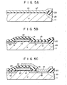
- a P type silicon substrate 11 of 1 to 100 ⁇ cm in resistivity is prepared.
- An impurity of the same conductivity type as that of the substrate 11 is doped by the ion implantation into a region in the substrate 11 which will serve as a field region.
- a field oxidation film 20 for separating the element regions from one another is formed to a thickness of approximately 6,000 A by the selective oxidation technique.
- a gate insulation film 21 of approximately 500 A in thickness is formed on the element region by the dry oxidation or the hydrochloride oxidation technique.
- a polysilicon layer 14' (or conductive layer) is formed to about 4,000 A in thickness over the entire surface of the gate insulation film 21 by the vapor phase growing process.
- the polysilicon layer 14' contains P-type or N-type impurity, and therefore is in low resistance.
- a layer 25 for preventing the formation of a parastic layer is formed underlying the field insulation film 20.
- the polysilicon layer 14' is patterned by the P EP (the photoengraving process), to form word lines 14 as gate electrodes.
- P EP the photoengraving process
- arsenide (As) is diffused u p to 10 2 0 to 10 21 /cm 3 in a surface concentration.
- arsenide is ion-implanted with a dose of about 10 1 5 to 10 16 cm- 2 .
- N + regions 12 and 13 are formed, which are respectively used as the source and drain of a MOS transistor.
- the semiconductor structure thus fabricated is again subjected to a dry oxidation at about 1,000°C, thereby to form a silicon oxide film 22 over the entire surface of the element region.
- an oxide film 23 (low temperature oxide film) is formed up to a thickness of approximately 2,000 to 3,000 A in a low temperature condition, laying over-the entire surface of the semiconductor structure.
- word lines i.e., gate electrode layers 14, are formed in the region between the N+ regions 12 and 13 of the substrate 11.
- the PEP technique is employed again to selectively remove the oxidation film 23 and the silicon oxidation film 22, and to form contact holes 15 at predetermined locations which open to expose the N + region 12.
- a second polysilicon layer or conductive layer is grown on the entire surface of the semiconductor structure by the vapor phase growing process.
- the polysilicon layer formed is patterned by the PEP process to have a desired polysilicon layer 16.
- the polysilicon layer 16 may be a polysilicon layer doped with phosphorour (P) or arsenide (As). Alternatively, a polysilicon layer undoped with impurity is first formed and then doped with arsenide by the implantation process.
- a low temperature oxidation film 24 of approximately 10,000 A in thickness is deposited on the entire surface of the semiconductor structure by the CVD process. Then, a contact hole 17 allowing the conductive layer 16 to be exposed is formed. An aluminum layer is deposited by the vacuum deposition process on the entire surface of the semiconductor structure. The aluminum layer is subjected to a patterning by the PEP technique to thereby form a data line 18 of a predetermined pattern. Finally, the semiconductor structure is covered with a protective film (not shown). At this point, the semiconductor memory device is completed.
- any impurity contained in the conductive layer 16 is diffused into the -region in the vicinity of the interface between N + region 12 and the field oxidation film 20. That is, the N region is formed in a substantial self-aligning manner. With the self-alignment of the N + region, even if the substrate 11 is partially exposed at the time of forming the contact hole 15, the second conductive layer 16 and the substrate 11 are not shortcircuited.
- Fig. 6 shows a cross sectional structure of another embodiment of a MOS according to the present invention.
- This illustrated structure corresponds to that of Fig. 4 in the first embodiment.
- Like numerals are used for simplicity to designate like or equivalent portions in Fig. 4.
- a feature of this embodiment lies in a configuration of the N + region 12 having a nonuniform thickness. Specifically, the thickness of the portion of the N + region 12 underlying the contact hole 15 is thicker than that of the remaining portion.
- an undoped polysilicon layer is deposited over the entire surface of the semiconductor structure in the process step for forming the conductive layer 16. Then, phosphorous is diffused into the region 12. Alternately, the region is doped with phosphbrous.
- a predetermined patterning is applied to the conductive layer 16.
- the heat treatment following the formation of the conductive layer 16 implants a larger amount of impurity from the conductive layer 16 into the N + region 12, when compared with that of the first embodiment. Therefore, the N + region 12 is grown to have a greater thickness.
- the polysilicon layer for the word line 14 may be replaced by a layer made of high melting point silicide, such as molybdenum silicide (MoSi2), a layer of high melting point metal, such as molybdenum (Mo), or a combination of the polysilicon layer and either of the latter two layers.
- the conductive layer 16 may be a high melting point silicide film.
- material for the conductive layer 16 may be any conductive material which may contain impurities, for example, high melting point silicide.
- the substrate material is of P type and the memory cells in the ROM are N channel MOS transistors.
- the substrate material may be of P type and the memory cells may be N well complementary MOS transistors.
- the substrate material may be of N type and the memory cells may be P well complementary MOS transistors with the P wells formed in the substrate.
- the present invention provides a ROM based on the contact method which has a reduced area for each memory cell and an improved integration density, and a method of manufacturing the ROM.
Landscapes
- Semiconductor Memories (AREA)
- Read Only Memory (AREA)
Applications Claiming Priority (2)
| Application Number | Priority Date | Filing Date | Title |
|---|---|---|---|
| JP75026/83 | 1983-04-28 | ||
| JP58075026A JPS59201461A (ja) | 1983-04-28 | 1983-04-28 | 読み出し専用半導体記憶装置およびその製造方法 |
Publications (3)
| Publication Number | Publication Date |
|---|---|
| EP0124115A2 true EP0124115A2 (de) | 1984-11-07 |
| EP0124115A3 EP0124115A3 (en) | 1986-10-08 |
| EP0124115B1 EP0124115B1 (de) | 1990-10-24 |
Family
ID=13564252
Family Applications (1)
| Application Number | Title | Priority Date | Filing Date |
|---|---|---|---|
| EP84104787A Expired - Lifetime EP0124115B1 (de) | 1983-04-28 | 1984-04-27 | Halbleiter-ROM-Anordnung und Herstellungsverfahren |
Country Status (4)
| Country | Link |
|---|---|
| US (2) | US4737835A (de) |
| EP (1) | EP0124115B1 (de) |
| JP (1) | JPS59201461A (de) |
| DE (1) | DE3483437D1 (de) |
Cited By (6)
| Publication number | Priority date | Publication date | Assignee | Title |
|---|---|---|---|---|
| EP0186855A3 (en) * | 1984-12-25 | 1986-10-08 | Kabushiki Kaisha Toshiba | Semiconductor read only memory device and method of manufacturing the same |
| EP0190928A3 (en) * | 1985-02-08 | 1987-08-19 | Kabushiki Kaisha Toshiba | Integrated mos transistor and method of manufacturing it |
| DE4005645A1 (de) * | 1989-02-22 | 1990-08-23 | Toshiba Kawasaki Kk | Mos-halbleiteranordnung |
| US5101262A (en) * | 1985-08-13 | 1992-03-31 | Kabushiki Kaisha Toshiba | Semiconductor memory device and method of manufacturing it |
| EP0429041A3 (en) * | 1989-11-20 | 1992-06-03 | Kabushiki Kaisha Toshiba | Semiconductor integrated circuit apparatus having programmable logic device |
| EP0514095A3 (de) * | 1991-05-16 | 1992-12-30 | AT&T Corp. | Integrierte Schaltung bestehend aus SRAM-Zellen |
Families Citing this family (15)
| Publication number | Priority date | Publication date | Assignee | Title |
|---|---|---|---|---|
| JPS5994454A (ja) * | 1982-11-19 | 1984-05-31 | Nec Kyushu Ltd | 半導体装置とその製造方法 |
| JPS61183954A (ja) * | 1985-02-08 | 1986-08-16 | Toshiba Corp | 読み出し専用半導体記憶装置の製造方法 |
| JPS61183953A (ja) * | 1985-02-08 | 1986-08-16 | Toshiba Corp | 読み出し専用半導体記憶装置 |
| JPS6237961A (ja) * | 1985-08-13 | 1987-02-18 | Toshiba Corp | 読み出し専用半導体記憶装置 |
| JPS6237960A (ja) * | 1985-08-13 | 1987-02-18 | Toshiba Corp | 読み出し専用半導体記憶装置の製造方法 |
| JPH06105778B2 (ja) * | 1985-08-15 | 1994-12-21 | 株式会社東芝 | 読み出し専用半導体記憶装置およびその製造方法 |
| JPS6240765A (ja) * | 1985-08-15 | 1987-02-21 | Toshiba Corp | 読み出し専用半導体記憶装置およびその製造方法 |
| JPS62101069A (ja) * | 1985-10-28 | 1987-05-11 | Toshiba Corp | 半導体装置の製造方法 |
| JPS63128750A (ja) * | 1986-11-19 | 1988-06-01 | Toshiba Corp | 半導体装置 |
| JPH01129440A (ja) * | 1987-11-14 | 1989-05-22 | Fujitsu Ltd | 半導体装置 |
| JPH01256125A (ja) * | 1988-04-05 | 1989-10-12 | Hitachi Ltd | 半導体集積回路装置の製造方法 |
| FR2634318B1 (fr) * | 1988-07-13 | 1992-02-21 | Commissariat Energie Atomique | Procede de fabrication d'une cellule de memoire integree |
| US5204276A (en) * | 1988-12-06 | 1993-04-20 | Kabushiki Kaisha Toshiba | Method of manufacturing semiconductor device |
| US5330924A (en) * | 1993-11-19 | 1994-07-19 | United Microelectronics Corporation | Method of making 0.6 micrometer word line pitch ROM cell by 0.6 micrometer technology |
| US5578873A (en) * | 1994-10-12 | 1996-11-26 | Micron Technology, Inc. | Integrated circuitry having a thin film polysilicon layer in ohmic contact with a conductive layer |
Family Cites Families (12)
| Publication number | Priority date | Publication date | Assignee | Title |
|---|---|---|---|---|
| JPS5915495B2 (ja) * | 1974-10-04 | 1984-04-10 | 日本電気株式会社 | 半導体装置 |
| US4475964A (en) * | 1979-02-20 | 1984-10-09 | Tokyo Shibaura Denki Kabushiki Kaisha | Method of manufacturing a semiconductor device |
| US4324238A (en) * | 1979-02-28 | 1982-04-13 | Abbott Laboratories | Equipment sets having a combined air barrier and liquid sequencing device for the sequential administration of medical liquids at dual flow rates |
| US4291322A (en) * | 1979-07-30 | 1981-09-22 | Bell Telephone Laboratories, Incorporated | Structure for shallow junction MOS circuits |
| GB2070329B (en) * | 1980-01-25 | 1983-10-26 | Tokyo Shibaura Electric Co | Semiconductor memory device |
| US4372031A (en) * | 1980-03-21 | 1983-02-08 | Texas Instruments Incorporated | Method of making high density memory cells with improved metal-to-silicon contacts |
| JPS56134757A (en) * | 1980-03-26 | 1981-10-21 | Nec Corp | Complementary type mos semiconductor device and its manufacture |
| US4341009A (en) * | 1980-12-05 | 1982-07-27 | International Business Machines Corporation | Method for making an electrical contact to a silicon substrate through a relatively thin layer of silicon dioxide on the surface of the substrate |
| US4403394A (en) * | 1980-12-17 | 1983-09-13 | International Business Machines Corporation | Formation of bit lines for ram device |
| JPS5827359A (ja) * | 1981-08-11 | 1983-02-18 | Fujitsu Ltd | 半導体記憶装置及びその製造方法 |
| JPS60116167A (ja) * | 1983-11-29 | 1985-06-22 | Toshiba Corp | 半導体記憶装置及びその製造方法 |
| HU194830B (en) * | 1984-10-05 | 1988-03-28 | Richter Gedeon Vegyeszet | Process for the production of derivatives of piridine |
-
1983
- 1983-04-28 JP JP58075026A patent/JPS59201461A/ja active Pending
-
1984
- 1984-04-27 DE DE8484104787T patent/DE3483437D1/de not_active Expired - Lifetime
- 1984-04-27 EP EP84104787A patent/EP0124115B1/de not_active Expired - Lifetime
-
1986
- 1986-10-16 US US06/919,556 patent/US4737835A/en not_active Expired - Lifetime
-
1988
- 1988-01-12 US US07/143,068 patent/US4855248A/en not_active Expired - Lifetime
Cited By (8)
| Publication number | Priority date | Publication date | Assignee | Title |
|---|---|---|---|---|
| EP0186855A3 (en) * | 1984-12-25 | 1986-10-08 | Kabushiki Kaisha Toshiba | Semiconductor read only memory device and method of manufacturing the same |
| US4755864A (en) * | 1984-12-25 | 1988-07-05 | Kabushiki Kaisha Toshiba | Semiconductor read only memory device with selectively present mask layer |
| EP0190928A3 (en) * | 1985-02-08 | 1987-08-19 | Kabushiki Kaisha Toshiba | Integrated mos transistor and method of manufacturing it |
| US5101262A (en) * | 1985-08-13 | 1992-03-31 | Kabushiki Kaisha Toshiba | Semiconductor memory device and method of manufacturing it |
| DE4005645A1 (de) * | 1989-02-22 | 1990-08-23 | Toshiba Kawasaki Kk | Mos-halbleiteranordnung |
| US5031011A (en) * | 1989-02-22 | 1991-07-09 | Kabushiki Kaisha Toshiba | MOS type semiconductor device |
| EP0429041A3 (en) * | 1989-11-20 | 1992-06-03 | Kabushiki Kaisha Toshiba | Semiconductor integrated circuit apparatus having programmable logic device |
| EP0514095A3 (de) * | 1991-05-16 | 1992-12-30 | AT&T Corp. | Integrierte Schaltung bestehend aus SRAM-Zellen |
Also Published As
| Publication number | Publication date |
|---|---|
| JPS59201461A (ja) | 1984-11-15 |
| US4737835A (en) | 1988-04-12 |
| EP0124115B1 (de) | 1990-10-24 |
| US4855248A (en) | 1989-08-08 |
| DE3483437D1 (de) | 1990-11-29 |
| EP0124115A3 (en) | 1986-10-08 |
Similar Documents
| Publication | Publication Date | Title |
|---|---|---|
| EP0124115B1 (de) | Halbleiter-ROM-Anordnung und Herstellungsverfahren | |
| EP0186855B1 (de) | Halbleiternurlesespeicheranordnung und Verfahren zu ihrer Herstellung | |
| US5352620A (en) | Method of making semiconductor device with memory cells and peripheral transistors | |
| US5338954A (en) | Semiconductor memory device having an insulating film and a trap film joined in a channel region | |
| US4630089A (en) | Semiconductor memory device | |
| US5656839A (en) | Semiconductor integrated circuit device having single-element type nonvolatile memory elements | |
| US4992389A (en) | Making a self aligned semiconductor device | |
| US4750024A (en) | Offset floating gate EPROM memory cell | |
| US5707884A (en) | Process for fabricating a contactless electrical erasable EPROM memory device | |
| JPH0864706A (ja) | 不揮発性半導体メモリ装置の製造方法 | |
| US4748492A (en) | Read only memory | |
| US5194924A (en) | Semiconductor device of an LDD structure having a floating gate | |
| US5113238A (en) | Contactless non-volatile memory array cells | |
| JPH0466106B2 (de) | ||
| JPH10335611A (ja) | 不揮発性メモリデバイス並びにその製造方法 | |
| US6150700A (en) | Advanced nor-type mask ROM | |
| US4825271A (en) | Nonvolatile semiconductor memory | |
| EP0145955B1 (de) | Nur-Lese-Speicheranordnung und Herstellungsverfahren | |
| US4441941A (en) | Method for manufacturing a semiconductor device employing element isolation using insulating materials | |
| US5227319A (en) | Method of manufacturing a semiconductor device | |
| US4874715A (en) | Read only memory with improved channel length control and method of forming | |
| US5027175A (en) | Integrated circuit semiconductor device having improved wiring structure | |
| JP2001007224A (ja) | 半導体装置及びその製造方法 | |
| JPH03194967A (ja) | 半導体不揮発性メモリの製造方法 | |
| US20030157758A1 (en) | Non-volatile semiconductor memory device and manufacturing method therefor |
Legal Events
| Date | Code | Title | Description |
|---|---|---|---|
| PUAI | Public reference made under article 153(3) epc to a published international application that has entered the european phase |
Free format text: ORIGINAL CODE: 0009012 |
|
| 17P | Request for examination filed |
Effective date: 19840427 |
|
| AK | Designated contracting states |
Designated state(s): DE FR GB IT |
|
| PUAL | Search report despatched |
Free format text: ORIGINAL CODE: 0009013 |
|
| AK | Designated contracting states |
Kind code of ref document: A3 Designated state(s): DE FR GB IT |
|
| 17Q | First examination report despatched |
Effective date: 19890215 |
|
| GRAA | (expected) grant |
Free format text: ORIGINAL CODE: 0009210 |
|
| AK | Designated contracting states |
Kind code of ref document: B1 Designated state(s): DE FR GB IT |
|
| ITF | It: translation for a ep patent filed | ||
| REF | Corresponds to: |
Ref document number: 3483437 Country of ref document: DE Date of ref document: 19901129 |
|
| ET | Fr: translation filed | ||
| ITTA | It: last paid annual fee | ||
| PLBE | No opposition filed within time limit |
Free format text: ORIGINAL CODE: 0009261 |
|
| STAA | Information on the status of an ep patent application or granted ep patent |
Free format text: STATUS: NO OPPOSITION FILED WITHIN TIME LIMIT |
|
| 26N | No opposition filed | ||
| PGFP | Annual fee paid to national office [announced via postgrant information from national office to epo] |
Ref country code: FR Payment date: 19970409 Year of fee payment: 14 |
|
| PGFP | Annual fee paid to national office [announced via postgrant information from national office to epo] |
Ref country code: GB Payment date: 19970418 Year of fee payment: 14 |
|
| PGFP | Annual fee paid to national office [announced via postgrant information from national office to epo] |
Ref country code: DE Payment date: 19970505 Year of fee payment: 14 |
|
| PG25 | Lapsed in a contracting state [announced via postgrant information from national office to epo] |
Ref country code: GB Free format text: LAPSE BECAUSE OF NON-PAYMENT OF DUE FEES Effective date: 19980427 |
|
| PG25 | Lapsed in a contracting state [announced via postgrant information from national office to epo] |
Ref country code: FR Free format text: THE PATENT HAS BEEN ANNULLED BY A DECISION OF A NATIONAL AUTHORITY Effective date: 19980430 |
|
| GBPC | Gb: european patent ceased through non-payment of renewal fee |
Effective date: 19980427 |
|
| PG25 | Lapsed in a contracting state [announced via postgrant information from national office to epo] |
Ref country code: DE Free format text: LAPSE BECAUSE OF NON-PAYMENT OF DUE FEES Effective date: 19990202 |
|
| REG | Reference to a national code |
Ref country code: FR Ref legal event code: ST |