EP0126525A1 - Verfahren zur Herstellung einer integrierten Schaltung mittels eines Gate-Arrays - Google Patents
Verfahren zur Herstellung einer integrierten Schaltung mittels eines Gate-Arrays Download PDFInfo
- Publication number
- EP0126525A1 EP0126525A1 EP84301898A EP84301898A EP0126525A1 EP 0126525 A1 EP0126525 A1 EP 0126525A1 EP 84301898 A EP84301898 A EP 84301898A EP 84301898 A EP84301898 A EP 84301898A EP 0126525 A1 EP0126525 A1 EP 0126525A1
- Authority
- EP
- European Patent Office
- Prior art keywords
- macro cells
- data
- cells
- expanded
- logic
- Prior art date
- Legal status (The legal status is an assumption and is not a legal conclusion. Google has not performed a legal analysis and makes no representation as to the accuracy of the status listed.)
- Ceased
Links
Images


Classifications
-
- G—PHYSICS
- G06—COMPUTING OR CALCULATING; COUNTING
- G06F—ELECTRIC DIGITAL DATA PROCESSING
- G06F30/00—Computer-aided design [CAD]
- G06F30/30—Circuit design
- G06F30/39—Circuit design at the physical level
Definitions
- This invention relates to a method for manufacturing a gate array integrated circuit device which comprises a logic system provided on a semiconductor substrate.
- a manufacturer prepares a master bulk pattern which includes basic dells in array form on a semiconductor substrate, prior to the submission of detailed design data for a particular logic system. After finishing the design of the logic system, the customer, i.e. system designer, supplies detailed design data, describing the particular logic system, to the manufacturer. Thereafter, the manufacturer produces a wiring pattern according to this logic system information and provides the wiring pattern on the semiconductor substrate which connects the basic cells.
- the "semi-custom" gate array technology has advantages in that the turn-around time on a design is very short, because the manufacturer only has to produce a wiring pattern. Moreover, although the manufacturing cost is lower than that of a full-custom integrated circuit device, the system designer still receives the originally designed integrated circuit device.
- An embodiment of the present invention can provide a method for manufacturing a gate array integrated circuit device, which simplifies the steps for designing logic systems.
- An embodiment of the present invention can provide a method for manufacturing a gate array integrated circuit device which reduces the turn-around time for designing the logic system by reducing the amount of data, which is required from the designer (i.e. customer), to describe the system, thereby reducing the cost of data storage, and ultimately the manufacturing cost.
- a gate array integrated circuit device which comprises a logic system formed on a semiconductor substrate, comprising the steps of:
- a new macro cell which comprises a plurality of macro cells and has a logic function which is more complex than that of a macro cell, is introduced for the design of a logic system.
- Symbol data for identifying the type of expanded macro cell and detailed data for identifying the included macro cells, the connection of the macro cells and the logic function thereof, are used to define the expanded macro cell.
- the logic function for each expanded macro cell can be that of a standard logic circuit known to the designers in the logic system design art.
- the symbol data and the detailed data for the expanded macro cells are stored in a semi-permanent memory, as are symbol data and detailed data for the macro cells.
- logic system data for the designed logic system, and this logic system data comprises only symbol data for the expanded macro cells, (some) macro cells, and their interconnections.
- the logic system data does not include the more complex detailed data.
- a conductive wiring pattern is then provided for the semiconductor substrate by synthesizing the logic system data (provided by the customer) and the detailed data (stored in semi-permanent memory).
- Fig. 1 is a plan view of a semiconductor substrate or chip 100 which is prepared by using a master bulk pattern.
- a large number of basic cells 101 are arranged on the substrate 100 in a basic cell array area 103, and input/output buffers 104 are located about the periphery of the basic cell array area 103.
- In the basic cell array area 103 there is a channel region 102 between rows of basic cells 101 where a conductive wiring pattern for interconnection of the electic elements in the basic cells 101 is arranged.
- Fig. 2 is a plan view of a master bulk pattern for two basic cells 101.
- diffused regions are produced in the surface of the semiconductor substrate for an input transistor Q 1 , an output transistor Q2, a Schottky diode Q 3 , a diode Q 4 , and resistors R 1 , R 2 , R 3 .
- At least Q 1 , Q 2 , Q 3 and Q 4 are active electrical elements.
- Vcc and GND are power supply lines.
- the first step is the manufacture of the basic cells 101 in the form of an array on the semiconductor substrate.
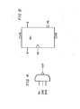
- Fig. 3 is a circuit diagram of a type of basic cell 101, wherein the electric circuit elements are interconnected; wherein Q 1 , Q 2 , Q 3 , Q 4 are the same as in Fig. 2; wherein Vcc and GND are power supplies; and wherein IN 1 , IN2, IN 3 are inputs and OUT is an output.
- the electric circuit elements e.g., transistors and resistors
- the basic cell 101 forms a basic gate as a result of the interconnection of the elements within the basic cell.
- This basic gate can exhibit a logic function, e.g. a NAND function.
- the simplest, and smallest, possible type of macro cell is formed by interconnecting the circuit elements of a single basic cell, so as to enable it to perform a logic function such as a 3-input NAND gate.
- Fig. 4 is a logic diagram of the macro cell of Fig. 3, that is, a 3-input NAND gate.
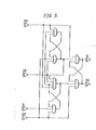
- Fig. 5 is a logic diagram of another type of macro cell.
- This macro cell comprises 6 basic cells, i.e. NAND gates, which are connected together so as to exhibit a logic function which, in this case, is a D-type flip-flop function.
- D is a data input
- CK is a clock input
- CR is a clear input
- PR is a preset input
- Q is an output
- XQ is a complementary output.
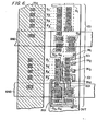
- Fig. 6 is a plan view of the wiring pattern for the macro cell of Fig. 4.
- the conductive wiring 301 is provided for connecting the electric elements (e.g. transistors and resistors) in the basic cell 101.
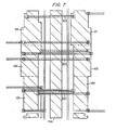
- Fig. 7 is a plan view of the wiring pattern of the macro cell of Fig. 5.
- conductive wiring 301 connects the electrical elements in 6 basic cells 101.
- the detailed circuitry of the basic cells 101 is omitted.
- Fig. 8 is a symbol for identifying the macro cell of Figs. 5 and 7, and includes a symbol name "FD1", input terminals and output terminals.
- Fig. 4 as well as being a logic diagram itself, is a symbol for identifying the macro cell of Fig. 6.
- the macro cell comprises one or more basic cells 101 and conductive wiring for interconnecting the electric elements, e.g., transistors, diodes and resistors, in the basic cells 101. Therefore, the macro cells each have some logic function, e.g., a 3-input NAND gate function, a D-type flip-flop function, etc...
- the logic functions of macro cells are generally simple and do not require a large number of basic cells 101. Examples of macro cells having particular logic functions, and the number of basic cells required to provide this function are listed in Table 1 below. In these examples, the macro cell units have no more than 12 basic cells. Therefore, the number of electric elements required to form any of these macro cells is less than 100.
- a second step in the manufacturing process is a step of storing, in a memory, symbol data representing the available symbols (e.g. Figs. 4 and 8) and storing corresponding detailed data regarding the connection of , the electric elements in the basic cells 101 of the macro cells and the logic functions for the macro cells.
- this detailed data comprises data representing the conductive wiring pattern (e.g. Figs. 6 and 7) for interconnecting the transistors Q 1 . Q 2 , diodes Q3' Q 4' resistors R 1 , R 2 , R 3 , and the power supplies Vcc, GND in the basic cells 101.
- a standard macro cell having a logic function such as one of those in Table 1, has a predetermined wiring pattern particular to that type of macro cell.
- Detailed data including data representing the wiring pattern, is stored in memory for all types of standard macro cells.
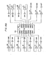
- Fig. 9 is a logic diagram of one example of an expanded macro cell.
- An expanded macro cell comprises a plurality of macro cells connected together by wiring.
- A0, B0, Bl, B2, C0, Cl, C2, DO ... Vl, V2, W0 are respectively macro cells which form the expanded macro cell in this example.
- Some of the macro cells in Fig. 9 are of types which comprise only one basic cell, others e.g. Nl, N2, P2, Q0, T2, U0, V2, W0, comprise a plurality of basic cells.
- the total number of macro cells in the expanded macro cell of Fig. 9 is 37, and the total number of basic cells is 61.
- OUCH, OUDH, RCOH are accessible terminals of the expanded macro cell for interfacing with an external circuit.
- the expanded macro cell of Fig. 9 has the logic function of a synchronous 4-bit counter which is a standard type of logic function.
- Fig. 10 illustrates a symbol for identifying the expanded macro cell of Fig. 9. As shown in Fig. 10, the shape of this expanded macro cell symbol 400 is a rectangle, and the name given to this particular type of expanded macro cell is "F161", which readily identifies the logic function as well as the expanded macro cell. In this type of symbol, the name is placed approximately at the center of the rectangle, and an index mark 401 indicates the orientation of the symbol 400 and appears at the top of the rectangle.
- the symbol 400 also includes the accessible terminals which can be used to interface with external macro cells and/or other expanded macro cells, and these accessible terminals have names for indicating the nature and property of the signals, for example, CLRL, CLKH, INAH, INBH, INCH, INDH, ENPH, RCOH, OUAH, OUBH, OUCH, OUDH, ENTH, LODL.
- the expanded macro cells have unique names of up to 4 characters, e.g., "F161," and in addition the accessible terminals have unique 4 character names, the last character being used to indicate whether the terminal is used as active-high or active-low, e.g.
- the third step is a step for storing, in a memory, symbol data representing the expanded macro cell symbols (Fig. 10), and also storing coresponding detailed data, including information about the connection of the macro cells which form the expanded macro cell, and about the logic functions.
- this detailed data includes, for each expanded macro cell, data identifying the macro cells which form the expanded macro cell, the terminals for interfacing the connections of these macro cells and the external terminals for connection to other expanded macro cells (see Fig. 9).
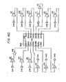
- Figs. 11 and 12 are, respectively, a logic diagram and a symbol for another example of an expanded macro cell.
- Each of the 13 macro cells K0, Kl, K2, L0, Ll, L2, M0, N0, Nl, N2, P0, Pl, and P2 comprises a single basic , cell, and each of the 10 macro cells T0, Tl, U0, Ul, V0, Vl, W0, Wl, X0, Xl comprises 2 basic cells. Therefore, this expanded macro cell comprises 23 macro cells (formed by 33 basic cells) connected together. It has a 4-line to 10-line decoder function, which is a standard and common logic function.
- the symbol 402 in Fig. 12 the name of this expanded macro cell ("F42") and the names of the terminals correspond to those in Fig. 10.
- the logic functions of the expanded macro cells are very standardized in this technological area, e.g., integrated logic circuit technology and logic system design technology.
- integrated logic circuit technology e.g., integrated logic circuit technology and logic system design technology.
- standard-technology TTL circuit devices e.g., Series 54/74, Series 54H/74H, Series 54LS/74LS, and Series 54S/74S, which are-very familiar to design engineers.
- Many integrated logic circuit device companies manufacture devices of the same logic function as the standard-technology TTL circuit devices disclosed in the above book.
- the expanded macro cells in Table 2 comprise at least 13 basic cells and 4 macro cells. Thereofre, they comprise at least 100 electric elements, and the expanded macro cell can thus be defined as an MSI (Medium Scale Integrated Circuit) macro cell, which means that the scale of this macro cell is the same as MSI.
- MSI Medium Scale Integrated Circuit
- a significant feature of the symbols for the expanded macro cells is that a portion of the name of each expanded macro cell, e.g. "F161", “F42” are identical to the names of the standard-technology TTL circuit devices, e.g. "SN74LS161", “SN74LS42” to which the expanded macro cell corresponds, thereby providing easy identification of the logic functions of the expanded macro cells.
- the order of the accessible and inaccessible terminals is the same as for the standard-technology TTL circuit device.
- An additional example of a symbol for an expanded macro cell is shown in Fig. 13.
- Fig. 14 illustrates an alternative type of symbol for representing the expanded macro cell of Fig. 13.
- the expanded macro cell symbols 404 (Fig. 13) and 406 (Fig. 14) is that, in the symbol 406, the name 407 (i.e., "F80") appears at the top of the rectangle instead of the index mark 405 which appears in the symbol 404. Therefore, the name 407 not only identifies the logic fnction of'the expanded macro cell, but also indicated the orientation of the symbol 406.
- expanded macro cells may also carry individual designations such as F0, F2, C3 for identification purposes in a particular logic system design (see, e.g. Fig. 16A).
- Figs. 16A - D form a logic diagram for an example of a logic system to be implemented on a gate array by the method of the present invention.
- This logic diagram comprises symbols for macro cells WO, X3, and for expanded macro cells 500, 501, 502, 503, the connections thereof, and the input/output terminals, but does not include complex logic diagrams for the logic within the expanded macro cells.
- This logic diagram also includes Input/Output Buffers D0, EO, M0, N0, etc.
- the logic system of Figs. 16A - D can be provided on one chip.
- the fourth step is a step for storing, in a memory, logic system data in accordance with the logic system design supplied by the customer.
- FIG. 16A - D shows how logic system data can be represented in a customer's design.
- the next step in the method of the present invention is to synthesize conductive wiring pattern data from the logic system data and the detailed data for the macro cells and the expanded macro cells, then to form a conductive wiring pattern for the semiconductor substrate to interconnect the electrical elements in the basic cells together.
- the conductive wiring pattern data specifies the interconnection of the basic cells, input/output buffers, and input/output pads, and includes the connections of Vcc and GND.
- an integrated circuit device for a logic system having very complicated logic circuits, a large number of gates, and a large number of electrical elements, can be manufactured.
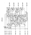
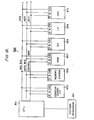
- Fig. 18 is a block diagram of a CAD (Computer Aided Design) system 800 for performing the method of the present invention.
- a CPU 801 is connected to peripheral apparatus, including a communication channel 805, a memory system 806, a disk memory 807, a magnetic tape memory 808, a line printer 809, and a CRT 810, via an address bus 802, a data bus 803, and a control bus 804.
- peripheral apparatus 805, 806, 807, 808, 809, 810 comprises its own interface circuit and controller therein (IF & CON) for communication with the CPU 801.
- the symbol data and detailed data for the macro cells and the expanded macro cells are stored in a first memory means, for example a disk memory 807 or a magnetic tape memory 808, that is, a semi-permanent memory apparatus.
- the logic system data is stored in a second memory means for example a memory system 806.
- the memory system 806 can be accessed much faster.
- the logic system data is different in each design because it depends upon the logic system which the system designer creates.
- the symbol data and the detailed data are always the same, because the types and functions of macro cells and standard expanded macro cells are predetermined. In other words, such data do not change, and are therefore suitable for storage in the semi-permanent first memory means.
- the second memory means 806 is more expensive than the first memory means 807, 808.
- the data stored in the second memory means 806- is only the logic system data (i.e. only symbol data for the selected macro cells and the expanded macro cells of the logic system, and the connections thereof), and not detailed data. Therefore, the area (capacity) required for storing the logic system data in the memory 806 can be minimal, and the cost of memory 806 can be minimised.
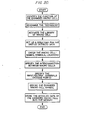
- Fig. 19 is a flow chart for a program for generating a data base for the detailed data representing each standard macro cell for storage in disk memory 807 or magnetic tape memory 808.
- a conventional graphics system can be used (e.g. the DESIGNER IV graphics system by Computer Vision Co. or the GDSII graphics system by Calma Co.).
- the program steps are outlined by the flow chart set forth in Fig. 19.
- the logic function of a macro cell for which detailed data is to be generated is specified, and the specific type of technology is selected from several gate array integrated circuit technologies.
- a library in the memory which stores data for the basic components (e.g. electric elements, transistor, resistor, diode, conductive wiring) is activated, and a directory (e.g. designating the space in the memory for storing the digitized detailed data) is set up.
- the next step is the entry of the basic components of the basic cells which form the macro cell.
- This step comprises entering identifiers for the basic cells and data representing the types of basic cells. For example, in one basic cell, all of the electric elements are used to form a 3-input NAND gate, while in another basic cell, only the input transistor is used to form additional input means for other basic cells.
- the input/output terminal for each basic cell is entered.
- the conductive wiring pattern which interconnects the electric elements and/or the input/output terminal of the basic cells is specified.
- the access points (i.e. terminals) of the macro cell are specified and the symbol for the macro cell is defined. These access points are used for interconnecting the macro cell to other macro cells or expanded macro cells.
- the actual mask pattern for the wiring layers of each standard macro cell which could be used in an integrated circuit device can be generated.
- the actual mask pattern is readily generated on the basis of the detailed data because the detailed data is so specific that it is almost at the same level as the mask pattern level and because the mask can be defined using data representing connecting straight lines.
- the circuit parameters of the macro cell are evaluated. These circuit parameters include, for example, the delay time, hold time, set-up time, etc.... which are necessary information for system design using the macro cells.
- the generated mask pattern data, the basic cell data, the access point data and the circuit parameters are stored in the disk memory 807 or the magnetic tape memory 808 (see Fig. 18) as detailed data for the macro cell.
- the mask pattern data and the access point data are graphic data, stored as digital data representing the actual mask pattern.
- the graphic data comprises precise data from which the actual mask pattern can be readily drawn. If the result of the evaluation is unacceptable, the macro cell is modified until an acceptable evaluation is obtained. The stored detailed data is maintained for read out as often as it is needed.
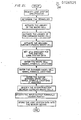
- Fig. 20 is a flow chart for program steps for storing the detailed data for an expanded macro cell to generate a data base for the standard expanded macro cells.
- the same conventional graphics system e.g. the above-mentioned DESIGNER IV or GDSII systems
- the function of the expanded macro cell for which data is to be stored is identified, thereby determining the technology and activating the library for the macro cells.
- a directory for the digital detailed data of the expanded macro cell is set up, and ,he information for the macro cells which form the expanded macro cell, is entered. This information includes the name (for identification), the symbol, the logic function and the location within the expanded macro cell as a whole.
- the interconnections (see Fig. 9) between the macro cells in the expanded macro cell are specified, as well as the input/output terminals of the expanded macro cell for the access points from the outside. Further, the symbol for the expanded macro cell is defined.
- the expanded macro cell does not require this type of predetermined wiring pattern data to be included in its detailed data, but has only interconnection information representing the connections between the macro cells, i.e. the interconnections at the logic diagram level (see, e.g., Fig. 9). Therefore, the actual wiring pattern of the expanded macro cell will be flexibly generated depending upon the nature of the detailed data for the macro cells forming the expanded macro cell.
- Fig. 21 is a flow chart for program steps for storing logic system data in accordance with a logic system design supplied by a customer. Again, a standard graphics system can be used for this step. After the type of logic system is identified, the technology is chosen and the libraries of the macro cells and the expanded macro cells (which are stored in the disk memory 807 and the magnetic tape memory 808) are activated. This may include so-called custom expanded macro cells, as explained later. Then a directory for digital logic system data is set up.
- the macro cells and expanded macro cells which are used in the logic system are entered, by inputting information including the name, symbol and location for each macro cell and expanded macro cell.
- the only macro cells which must be specified are those which are not included within a specified expanded, macro cell.
- the connections of the macro cells and the expanded macro cells are specified (e.g., see Figs. 16A - D); and then the input/output terminals which will correspond to the I/O pads of the chip are specified.
- the logic system data which is digitized and stored in the memory system 806, is at the logic diagram level, as illustrated, for example, by Figs. 16A - D.
- the digitizing step is simply the step of converting the information concerning the expanded macro cell name, symbol and location, I/O terminals and the connections, into corresponding digital data.
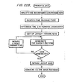
- Fig. 22A, 22B are flow charts for the program steps performed by the CPU 801 in generating the conductive wiring pattern after the logic system data is stored in the memory system 806.
- the technology is determined and the CPU 801 loads the logic system data from the memory system 806 and activates the libraries for the detailed data for the macro cells and expanded macro cells.
- the next step for the CPU 801 is to combine three sets of graphic data, i.e. the detailed data for the macro cells, the detailed data for the expanded macro cells, and the logic system data. This combined graphic data is converted into a machine language data base which the CPU 801 can understand.
- the logic system data must be expanded into NAND gates to establish a tree-structure data base which comprises the NAND gates and the connections thereof.
- the tree-structure data base is used for a violation check and logic simulation.
- the violation check looks for open terminals, fan-in, fan-out, driving factor, basic cell locations, total basic cell count, power dissipation and so forth.
- the logic simulaton ensures that the output result, based upon the input data prepared by the designer, is the same as the output data expected by the designer. If the result of these checks is unacceptable, the CPU 801 outputs an error message. If the result is acceptable, the CPU 801 proceeds to the next step.
- an interconnection parameter (which is a rule for interconnection) is specified; the package type used for the logic system is identified; and the assignment of the input/output terminals is determined.
- the CPU 801 sets up the layout pattern parameters from which the actual mask layout pattern can be generated.
- the layout pattern is generated based upon the layout pattern parameters. In this step, if the CPU 801 cannot generate the appropriate layout pattern (i.e., by using standard CAD techniques), the layout parameters (i.e. the above information) are modified.
- the layout map (similar to Fig. 7) which is a kind of image of the actual mask pattern, is provided. Then, the layout map is converted into the actual mask pattern i.e. the conductive wiring pattern (see e.g. Fig. 6) by a pattern generator 811.
- the pattern generator 811 can be any standard mask pattern generator, for example the model PG3600 by GCA. Once the pattern generator 811 has generated the actual mask pattern, the actual wiring can be readily deposited on the chip. Of course, once the CPU 801 has generated the layout map, there are a number of possible ways to process the layout map data. For example, the layout map data could be stored on a magnetic tape or disk which could then be transported for use with a pattern generator 811. Alternatively, the layout map data generated by the CPU 801 could be used to define the wiring pattern by using a light beam (for example, an ultraviolet light beam) and an acousto-optic modulator for modulating the light beam in accordance with the layout map data.
- a light beam for example, an ultraviolet light beam
- acousto-optic modulator for modulating the light beam in accordance with the layout map data.
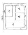
- Fig. 17A illustrates schematically an example of.a chip layout for a logic system in accordance with a conductive wiring pattern generated by the method of the present invention; where input/output buffers 104 are located about the periphery of the basic cell array area 103. As shown in Fig. 17A, each expanded macro cell (F161, F80, F42) is located in the array area 103.
- Fig. 17B is a schematic plan view of the wiring pattern corresponding to an example of the wiring pattern for a portion of the layout map of Fig. 17A.
- the expanded macro cells of the present invention are more complex and functionally sophisticated than prior art macro cells. In addition, they have commonly known and standardized logic functions. But since the expanded macro cells include numerous basic cells connected together, they sometimes have poor gate usage efficiency, depending on the particular logic system. There is no efficiency or redundancy problem if the expanded macro cells used by customers or designers in the logic system are exactly the same as the standard expanded macro cells in the library. However, poor efficiency in use of the expanded macro cells will occur when designers want to use circuits in the logic system which are not the same as the standard expanded macro cells; for example, where part of the expanded macro cell, (e.g. one or more of the terminals, wirings, or macro cells in the expanded macro cell) is not used. In that situation, there will also be waste of area on the semiconductor substrate, because the area which will actually be used in the expanded macro cell is smaller than the prepared area which it will occupy on the semiconductor substrate.
- part of the expanded macro cell e.g. one or more of the terminals, wirings, or macro cells in the expanded macro cell
- the systems designer is allowed to alter an expanded macro cell in order to optimize the logic function, the circuit performance, and the usage of area.
- the input and output terminals of a standard expanded macro cell are not to be used entirely, it is recommended that the unused terminals and wiring (and the macro cells which are attached to the unused terminals) be eliminated.
- This kind of flexibility in altering the standard expanded macro cell improves its effective use of the occupied area, and also the power consumption and electrical characteristics. If at least one terminal, wiring, or macro cell is eliminated from a standard expanded macro cell, the resulting expanded macro cell is called a custom expanded macro cell.
- Fig. 15 is a logic diagram of a custom expanded macro cell corresponding to an altered version of the standard expanded macro cell of Figs. 11, 12. As shown in Fig. 15, two output terminals "008L,” “009L,” three macro cells Xl, X0, P2 (which are equivalent to a total of 6 basic cells), and related wiring are eliminated from the expanded macro cell "F42" of Figs. 11, 12. In Fig. 16C, a symbol for identifying the custom expanded macro cell in Fig. 15 is used in the logic diagram of the logic system. This symbol is almost the same as the corresponding symbol for the standard expanded macro cell of Fig. 12.
- the expanded macro cell is a standard expanded macro cell or a custom expanded macro cell depending upon whether unused terminals exist.
- the detailed data of an expanded macro cell is constructed in such a way that unused terminals, macro cells and wiring can be easily eliminated without altering the significant portion of the logic function, to leave the detailed data for the custom expanded macro cell. This elimination procedure can be fully automated with CAD support or can be modified manually.
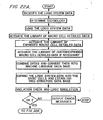
- Fig. 23 is a flow chart for program steps for storing data for a custom expanded macro cell.
- the logic function of the custom expanded macro cell is identified; the appropriate technology is determined; the library of the expanded macro cells is activated; and the directory for the detailed data is set up.
- the detailed data of the standard expanded macro cell from which the custom expanded macro celll will be created is entered.
- the custom expanded macro cell is created by eliminating the data for the unused terminals, macro cells and wiring, from the detailed data of the standard expanded macro cell.
- the structure of he detailed data is, for example, the binary tree-structure in which it is easy to eliminate this data without modifying the rest of the data accordingly.
- the input/output terminals are specified.
Landscapes
- Engineering & Computer Science (AREA)
- Computer Hardware Design (AREA)
- Physics & Mathematics (AREA)
- Theoretical Computer Science (AREA)
- Evolutionary Computation (AREA)
- Geometry (AREA)
- General Engineering & Computer Science (AREA)
- General Physics & Mathematics (AREA)
- Design And Manufacture Of Integrated Circuits (AREA)
- Semiconductor Integrated Circuits (AREA)
Applications Claiming Priority (2)
| Application Number | Priority Date | Filing Date | Title |
|---|---|---|---|
| US477751 | 1983-03-22 | ||
| US06/477,751 US4584653A (en) | 1983-03-22 | 1983-03-22 | Method for manufacturing a gate array integrated circuit device |
Publications (1)
| Publication Number | Publication Date |
|---|---|
| EP0126525A1 true EP0126525A1 (de) | 1984-11-28 |
Family
ID=23897213
Family Applications (1)
| Application Number | Title | Priority Date | Filing Date |
|---|---|---|---|
| EP84301898A Ceased EP0126525A1 (de) | 1983-03-22 | 1984-03-21 | Verfahren zur Herstellung einer integrierten Schaltung mittels eines Gate-Arrays |
Country Status (3)
| Country | Link |
|---|---|
| US (1) | US4584653A (de) |
| EP (1) | EP0126525A1 (de) |
| JP (1) | JPH0695568B2 (de) |
Cited By (3)
| Publication number | Priority date | Publication date | Assignee | Title |
|---|---|---|---|---|
| GB2213967A (en) * | 1988-01-13 | 1989-08-23 | Ricoh Kk | Knowledge based method and apparatus for designing integrated circuits using functional specifications |
| EP0368625A3 (de) * | 1988-11-08 | 1991-07-03 | Fujitsu Limited | Verfahren und Gerät zur Bildung eines Pattern-Layouts einer integrierten Halbleiterschaltung |
| US5348902A (en) * | 1992-01-21 | 1994-09-20 | Hitachi, Ltd. | Method of designing cells applicable to different design automation systems |
Families Citing this family (44)
| Publication number | Priority date | Publication date | Assignee | Title |
|---|---|---|---|---|
| JPH065541B2 (ja) * | 1983-12-30 | 1994-01-19 | 株式会社日立製作所 | 論理回路の自動設計方法 |
| JPH0673363B2 (ja) * | 1984-07-02 | 1994-09-14 | 株式会社東芝 | システムlsiの設計方法 |
| JPS6124250A (ja) * | 1984-07-13 | 1986-02-01 | Nippon Gakki Seizo Kk | 半導体集積回路装置 |
| US4858175A (en) * | 1984-09-29 | 1989-08-15 | Kabushiki Kaisha Toshiba | Monolithic semi-custom IC having standard LSI sections and coupling gate array sections |
| US4774559A (en) * | 1984-12-03 | 1988-09-27 | International Business Machines Corporation | Integrated circuit chip structure wiring and circuitry for driving highly capacitive on chip wiring nets |
| US4700316A (en) * | 1985-03-01 | 1987-10-13 | International Business Machines Corporation | Automated book layout in static CMOS |
| US4701860A (en) * | 1985-03-07 | 1987-10-20 | Harris Corporation | Integrated circuit architecture formed of parametric macro-cells |
| US4775942A (en) * | 1985-12-09 | 1988-10-04 | International Business Machines Corporation | Seed and stitch approach to embedded arrays |
| JPS62159278A (ja) * | 1986-01-08 | 1987-07-15 | Hitachi Ltd | 自動論理設計システム |
| JPS62189739A (ja) * | 1986-02-17 | 1987-08-19 | Hitachi Ltd | 半導体集積回路装置 |
| AU7728187A (en) * | 1986-09-12 | 1988-03-17 | Digital Equipment Corporation | Cad of logic circuits: rule structure for inserting new elements |
| US5175696A (en) * | 1986-09-12 | 1992-12-29 | Digital Equipment Corporation | Rule structure in a procedure for synthesis of logic circuits |
| US5212650A (en) * | 1986-09-12 | 1993-05-18 | Digital Equipment Corporation | Procedure and data structure for synthesis and transformation of logic circuit designs |
| US5267175A (en) * | 1986-09-12 | 1993-11-30 | Digital Equipment Corporation | Data base access mechanism for rules utilized by a synthesis procedure for logic circuit design |
| US5222029A (en) * | 1986-09-12 | 1993-06-22 | Digital Equipment Corporation | Bitwise implementation mechanism for a circuit design synthesis procedure |
| US5097422A (en) * | 1986-10-10 | 1992-03-17 | Cascade Design Automation Corporation | Method and apparatus for designing integrated circuits |
| US4849928A (en) * | 1987-01-28 | 1989-07-18 | Hauck Lane T | Logic array programmer |
| JPH0815210B2 (ja) * | 1987-06-04 | 1996-02-14 | 日本電気株式会社 | マスタスライス方式集積回路 |
| US4815003A (en) * | 1987-06-19 | 1989-03-21 | General Electric Company | Structured design method for high density standard cell and macrocell layout of VLSI chips |
| US4852015A (en) * | 1987-06-24 | 1989-07-25 | Eta Systems, Inc. | Automatic circuit layout router |
| US5119313A (en) * | 1987-08-04 | 1992-06-02 | Texas Instruments Incorporated | Comprehensive logic circuit layout system |
| US5150309A (en) * | 1987-08-04 | 1992-09-22 | Texas Instruments Incorporated | Comprehensive logic circuit layout system |
| US4951221A (en) * | 1988-04-18 | 1990-08-21 | General Electric Company | Cell stack for variable digit width serial architecture |
| US5173864A (en) * | 1988-08-20 | 1992-12-22 | Kabushiki Kaisha Toshiba | Standard cell and standard-cell-type integrated circuit |
| JPH02189477A (ja) * | 1989-01-19 | 1990-07-25 | Mitsubishi Electric Corp | 電子回路の測定仕様作成方法 |
| US5202841A (en) * | 1989-07-14 | 1993-04-13 | Mitsubishi Denki Kabushiki Kaisha | Layout pattern verification system |
| US5448494A (en) * | 1989-12-20 | 1995-09-05 | Fujitsu Limited | Mask data processing apparatus for integrated circuit production |
| JP2509755B2 (ja) * | 1990-11-22 | 1996-06-26 | 株式会社東芝 | 半導体集積回路製造方法 |
| US5283753A (en) * | 1991-07-25 | 1994-02-01 | Motorola, Inc. | Firm function block for a programmable block architected heterogeneous integrated circuit |
| JPH05274390A (ja) * | 1992-03-30 | 1993-10-22 | Matsushita Electric Ind Co Ltd | 回路素子割り付け方法及び遅延最適化方法並びに論理設計システム |
| US6675361B1 (en) | 1993-12-27 | 2004-01-06 | Hyundai Electronics America | Method of constructing an integrated circuit comprising an embedded macro |
| US5671397A (en) * | 1993-12-27 | 1997-09-23 | At&T Global Information Solutions Company | Sea-of-cells array of transistors |
| IL111708A (en) * | 1994-11-21 | 1998-03-10 | Chip Express Israel Ltd | Mapping of gate arrays |
| US5682323A (en) * | 1995-03-06 | 1997-10-28 | Lsi Logic Corporation | System and method for performing optical proximity correction on macrocell libraries |
| US5633807A (en) * | 1995-05-01 | 1997-05-27 | Lucent Technologies Inc. | System and method for generating mask layouts |
| US5754826A (en) * | 1995-08-04 | 1998-05-19 | Synopsys, Inc. | CAD and simulation system for targeting IC designs to multiple fabrication processes |
| US6453447B1 (en) | 1999-08-19 | 2002-09-17 | Aeroflex Utmc Microelectronic Systems Inc. | Method for fabricating integrated circuits |
| US6483131B1 (en) * | 2000-01-11 | 2002-11-19 | Texas Instruments Incorporated | High density and high speed cell array architecture |
| JP5028714B2 (ja) * | 2001-03-30 | 2012-09-19 | 富士通セミコンダクター株式会社 | 半導体集積回路装置、および配線方法 |
| US6910199B2 (en) * | 2001-04-23 | 2005-06-21 | Telairity Semiconductor, Inc. | Circuit group design methodologies |
| US20040010652A1 (en) * | 2001-06-26 | 2004-01-15 | Palmchip Corporation | System-on-chip (SOC) architecture with arbitrary pipeline depth |
| US7047175B1 (en) * | 2001-11-16 | 2006-05-16 | Synopsys, Inc. | System and method for enhancing the speed of dynamic timing simulation using delay assessment at compile time |
| US7448012B1 (en) | 2004-04-21 | 2008-11-04 | Qi-De Qian | Methods and system for improving integrated circuit layout |
| US11450605B2 (en) * | 2021-02-11 | 2022-09-20 | Taiwan Semiconductor Manufacturing Company, Ltd. | Reducing internal node loading in combination circuits |
Family Cites Families (4)
| Publication number | Priority date | Publication date | Assignee | Title |
|---|---|---|---|---|
| JPS588588B2 (ja) * | 1975-05-28 | 1983-02-16 | 株式会社日立製作所 | 半導体集積回路 |
| JPS60953B2 (ja) * | 1977-12-30 | 1985-01-11 | 富士通株式会社 | 半導体集積回路装置 |
| US4377849A (en) * | 1980-12-29 | 1983-03-22 | International Business Machines Corporation | Macro assembler process for automated circuit design |
| US4484292A (en) * | 1981-06-12 | 1984-11-20 | International Business Machines Corporation | High speed machine for the physical design of very large scale integrated circuits |
-
1983
- 1983-03-22 US US06/477,751 patent/US4584653A/en not_active Expired - Lifetime
-
1984
- 1984-03-21 JP JP59054108A patent/JPH0695568B2/ja not_active Expired - Lifetime
- 1984-03-21 EP EP84301898A patent/EP0126525A1/de not_active Ceased
Non-Patent Citations (12)
| Title |
|---|
| ELECTRICAL DESIGN NEWS, vol. 27, no. 15, 4 August 1982, Boston, USA A. RAPPAPORT "Automated design and simulation aids speed semicustom-IC development", pages 35-48 * |
| ELECTRO/80 CONFERENCE RECORD, vol. 5, 13-15 May 1980, Boston, USA R.KING "Using MECL 10K macrocell array as a basic building block for standard product development", pages 1-7 * |
| ELECTRONICS INTERNATIONAL * |
| ELECTRONICS INTERNATIONAL, vol. 54, no. 1, 13 January 1981, New York, USA R.A. ARMSTRONG "Applying CAD to gate arrays speeds 32-bit minicomputer design", pages 167-173 * |
| ELECTRONICS INTERNATIONAL, vol. 54, no. 14, 14 July 1981, New York, USA R. HORTON et al. "Design automation speeds through customization of logic arrays", pages 132-137 * |
| ELECTRONICS INTERNATIONAL, vol. 54, no. 24, 30 November 1981, New York, USA J.S. KOFORD et al. "Gate-array development system speeds designs to market", pages 116-120 * |
| ELECTRONICS INTERNATIONAL, vol. 54, no. 24, 30 November 1981, New York, USA M. DICKENS et al. "Graphics editor constructs standard cells, symbolizes subsystems", pages 121-125 * |
| ELECTRONICS INTERNATIONAL, vol. 56, no. 1, 13 January 1983, New York, USA B. GLADSTONE "Work station saves system design time", pages 173-177 * |
| FUJITSU - SCIENTIFIC AND TECHNICAL JOURNAL, vol. 18, no. 3, September 1982, Kawasaky, JP, T. SAITO et al. "A CAD system for logic design based on frames and demons", pages 437-451 * |
| PROCEEDINGS OF THE IEEE, vol. 71, no. 1, January 1983 T. SUDO et al. "CAD systems for VLSI in Japan", pages 129-143 * |
| WESCON TECHNICAL PAPER, vol. 26, September 1982 J. MARTIN "A new generation of silicon gate CMOS arrays", pages 1-10 * |
| WESCON TECHNICAL PAPER, vol. 26, September 1982 K.R. LOBO et al. "The LSI development system-I (LDS I) - A year of maturity", pages 1-6 * |
Cited By (5)
| Publication number | Priority date | Publication date | Assignee | Title |
|---|---|---|---|---|
| GB2213967A (en) * | 1988-01-13 | 1989-08-23 | Ricoh Kk | Knowledge based method and apparatus for designing integrated circuits using functional specifications |
| GB2213967B (en) * | 1988-01-13 | 1992-06-17 | Ricoh Kk | Knowledge based method for designing integrated circuits using functional specifications and fabricating masks for the production of such circuits. |
| EP0368625A3 (de) * | 1988-11-08 | 1991-07-03 | Fujitsu Limited | Verfahren und Gerät zur Bildung eines Pattern-Layouts einer integrierten Halbleiterschaltung |
| US5247456A (en) * | 1988-11-08 | 1993-09-21 | Fujitsu Limited | Method and apparatus for forming layout pattern of semiconductor integrated circuit |
| US5348902A (en) * | 1992-01-21 | 1994-09-20 | Hitachi, Ltd. | Method of designing cells applicable to different design automation systems |
Also Published As
| Publication number | Publication date |
|---|---|
| JPS59175749A (ja) | 1984-10-04 |
| US4584653A (en) | 1986-04-22 |
| JPH0695568B2 (ja) | 1994-11-24 |
Similar Documents
| Publication | Publication Date | Title |
|---|---|---|
| EP0126525A1 (de) | Verfahren zur Herstellung einer integrierten Schaltung mittels eines Gate-Arrays | |
| US4377849A (en) | Macro assembler process for automated circuit design | |
| US5253181A (en) | Programmable one-board computer, and methods of verification of logic circuit and alteration to actual circuit using the programmable one-board computer | |
| US6574786B1 (en) | Gate array cell generator using cadence relative object design | |
| KR102407458B1 (ko) | 집적회로 레이아웃을 생성하는 방법 | |
| Vai | VLSI design | |
| US5689432A (en) | Integrated circuit design and manufacturing method and an apparatus for designing an integrated circuit in accordance with the method | |
| US6083271A (en) | Method and apparatus for specifying multiple power domains in electronic circuit designs | |
| CN101196946B (zh) | 用于支持设计电路的方法、装置及印刷电路板制造方法 | |
| US5418733A (en) | Floor-planning apparatus for hierarchical design of LSI | |
| US5187784A (en) | Integrated circuit placement method using netlist and predetermined ordering constraints to produce a human readable integrated circuit schematic diagram | |
| US4960724A (en) | Method for deleting unused gates and method for manufacturing master-slice semiconductor integrated circuit device using the deleting method | |
| US5625565A (en) | System and method for generating a template for functional logic symbols | |
| JPH04124855A (ja) | 半導体集積回路装置とそのレイアウト設計方法及びレイアウト設計装置 | |
| US20080109782A1 (en) | Method and system for pin assignment | |
| Mattison | A high quality, low cost router for MOS/LSI | |
| US4602339A (en) | Method of manufacturing master-slice integrated circuit device | |
| KR20040036283A (ko) | 집적회로 장치 설계용 네트리스트 작성 방법 | |
| JP3824203B2 (ja) | 電気電子回路の結線図作成装置 | |
| US5841157A (en) | Semiconductor integrated circuit including a high density cell | |
| Biederman | An overview on writing a VHDL testbench | |
| Farlow | Machine aids to the design of ceramic substrates containing integrated circuit chips | |
| Falk | Tools II/Design techniques: Design for production: The computer steps in to automate physical design and testing of computers and other electronic equipment | |
| JPH0794589A (ja) | 半導体設計方法及び半導体設計装置 | |
| JPH01154279A (ja) | 半導体装置の製造方法 |
Legal Events
| Date | Code | Title | Description |
|---|---|---|---|
| PUAI | Public reference made under article 153(3) epc to a published international application that has entered the european phase |
Free format text: ORIGINAL CODE: 0009012 |
|
| AK | Designated contracting states |
Designated state(s): DE FR GB |
|
| 17P | Request for examination filed |
Effective date: 19841126 |
|
| STAA | Information on the status of an ep patent application or granted ep patent |
Free format text: STATUS: THE APPLICATION HAS BEEN REFUSED |
|
| 18R | Application refused |
Effective date: 19900806 |
|
| APAF | Appeal reference modified |
Free format text: ORIGINAL CODE: EPIDOSCREFNE |
|
| RIN1 | Information on inventor provided before grant (corrected) |
Inventor name: OHBA, OSAMC Inventor name: CHIH, SAMUEL |