EP0126977A1 - Plattenlaufwerk für flexible Platten - Google Patents
Plattenlaufwerk für flexible Platten Download PDFInfo
- Publication number
- EP0126977A1 EP0126977A1 EP84104628A EP84104628A EP0126977A1 EP 0126977 A1 EP0126977 A1 EP 0126977A1 EP 84104628 A EP84104628 A EP 84104628A EP 84104628 A EP84104628 A EP 84104628A EP 0126977 A1 EP0126977 A1 EP 0126977A1
- Authority
- EP
- European Patent Office
- Prior art keywords
- signal
- floppy disk
- disk drive
- inhibiting
- circuit
- Prior art date
- Legal status (The legal status is an assumption and is not a legal conclusion. Google has not performed a legal analysis and makes no representation as to the accuracy of the status listed.)
- Withdrawn
Links
- 230000004044 response Effects 0.000 abstract description 17
- 230000002401 inhibitory effect Effects 0.000 abstract description 3
- 238000012545 processing Methods 0.000 description 6
- 230000004048 modification Effects 0.000 description 3
- 238000012986 modification Methods 0.000 description 3
- 230000001960 triggered effect Effects 0.000 description 3
- 238000010586 diagram Methods 0.000 description 2
- 238000003780 insertion Methods 0.000 description 2
- 230000037431 insertion Effects 0.000 description 2
- 239000003990 capacitor Substances 0.000 description 1
- 101150069022 dss-1 gene Proteins 0.000 description 1
- 230000006870 function Effects 0.000 description 1
Images


Classifications
-
- G—PHYSICS
- G11—INFORMATION STORAGE
- G11B—INFORMATION STORAGE BASED ON RELATIVE MOVEMENT BETWEEN RECORD CARRIER AND TRANSDUCER
- G11B19/00—Driving, starting, stopping record carriers not specifically of filamentary or web form, or of supports therefor; Control thereof; Control of operating function ; Driving both disc and head
- G11B19/02—Control of operating function, e.g. switching from recording to reproducing
- G11B19/12—Control of operating function, e.g. switching from recording to reproducing by sensing distinguishing features of or on records, e.g. diameter end mark
Definitions
- the present invention relates to a floppy disk drive apparatus.
- a data processing system in which a plurality of floppy disk drive devices FDD-1 to FDD-N are coupled to a host computer HC. These floppy disk drive devices FDD-1 to FDD-N are selectively driven in response to drive select signals DSS-1 to DSS-N from the host computer HC.
- a disk drive motor of the floppy disk drive device thus selected is rotated in response to a motor drive signal MDS from the host computer HC, thereby enabling the data read out from the floppy disk to be transferred to the host computer HC and the data from the host computer HC to be written info the floppy disk.
- the motor drive signal MDS from the host computer HC is supplied not only to the floppy disk drive device selected but also to other nonselected floppy disk drive devices. Therefore, the disk drive motors of all the floppy disk drive devices can be driven in response to the motor drive signal MDS irrespective of whether the floppy disk is inserted or not, which causes the service lives of these disk drive motors to be shortened and the electric power consumption to be needlessly increased.
- a floppy disk drive apparatus comprising: a disk holding member for holding a floppy disk; a disk drive section which is driven in response to a drive signal, thereby rotating the disk holding member; a head section for writing data into this floppy disk and reading out the data therefrom; and a control section for inhibiting the supply of the drive signal to the disk drive section when it is detected that the floppy disk is not held on the disk holding member.
- the supply of the drive signal for allowing the disk drive section to be driven is cut off; therefore, when no floppy disk is inserted, this disk drive section is not driven, thereby preventing the service life of this disk drive section from being needlessly shortened.
- Figs. 2 and 3 illustrate a schematic top plan view and a side elevational view of a floppy disk drive apparatus according to one embodiment of the present invention.
- This floppy disk drive apparatus includes: a front panel 2 having a disk receiving portion; a clamping arm 4 for fixing a'floppy disk 6 inserted through this disk receiving portion on a spindle 8; a motor 10 for rotating this spindle 8; a recording/reproducing head 12; and a motor 14 for driving this recording/reproducing head 12 step by step in the radial direction of the floppy disk 6.
- This floppy disk drive apparatus further includes an index hole detector 16 for detecting an index hole of the floppy disk 6 and a disk detector 18 for detecting that the floppy disk 6 is inserted. Each of these detectors 16 and 18 has, for example, a light-emitting section and a photo-sensing section.
- the floppy disk 6 has a recording medium 6A and a casing 6B for enclosing this recording medium 6A.
- the recording medium 6A and casing 6B are formed with holes 6C adapted to be engaged with the spindle 8 at their centers, and at the same time index holes 6D are also formed.
- this casing 6B is formed with an opening portion 6E for enabling the recording medium 6A to be brought into contact with the head 12.
- Fig. 5 shows a control circuit to control the operation of the motor 10.
- the disk detector 18 includes a light-emitting diode 18D and a phototransistor 18T.
- the light-emitting diode 18D and phototransistor 18T are coupled to a power source terminal +V1 through respective resistors Rl and R2.
- a collector of the phototransistor 18T is coupled to an A input terminal of a monostable multivibrator 20 through an inverter 21 and is also coupled to one input terminal of an input inverting type AND gate 22.
- a motor drive signal from a motor drive signal generator 24 such as a host computer or the like is supplied to the other input terminal of this AND gate 22.
- An output terminal of the AND gate 22 together with a Q output terminal of the monostable multivibrator 20 is coupled through an OR gate 26 to a motor driver 28 for driving the motor 10. Namely, when the disk detector 18 detects that the floppy disk 6 is not inserted and generates a low level signal, the AND gate 22 functions to inhibit the motor drive signal from the motor drive signal generator-24 from being supplied to the motor driver 28.
- An initial resetting circuit 30 coupled to an R input terminal of the monostable multivibrator 20 resets this monostable multivibrator 20 when a power source is turned on and a power source voltage is supplied to the power source terminal +V1.
- the collector voltage of the phototransistor 18T changes from a low level to a high level, and the output voltage of the inverter 21 varies from a high level to a low level; thus, the monostable multivibrator 20 is driven, and a "1" level signal is generated from the Q output terminal of this monostable multivibrator 20 for a predetermined time. Due to this, the motor 10 is rotated for this predetermined time, thereby allowing the spindle 8 to be rotated and enabling the floppy disk 6 to be appropriately set on this spindle 8.
- Fig. 6 is a schematic side elevational view illustrating a floppy disk drive apparatus according to another embodiment of the present invention, in which a microswitch 40 is used in place of the disk detector 18. One end of this microswitch 40 is grounded and the other end is coupled to the power source +V1 through a resistor and to the input terminal of the inverter 21.
- the microswitch 40 when the floppy disk 6 is inserted and the clamping arm 4 is set into the closed position, the microswitch 40 is turned off, so that a high level voltage is applied to the inverter 21. On the other hand, when this clamping arm 40 is in the open position, the microswitch 40 is held in the ON state, so that a low level voltage is applied to the inverter 21.
- the floppy disk drive apparatus shown in Fig. 6 operates in the manner similar to the embodiment shown in Figs. 2 to 5 except that the operation of the motor 10 is controlled in dependence upon the closure or opening of the clamping arm 4 instead of whether the floppy disk 6 is inserted or not.
- Fig. 7 relates to another embodiment of the present invention and shows a motor control circuit of the floppy disk drive apparatus in which the disk detector 18 is omitted and the insertion of the floppy disk 6 is detected by the index hole detector 16.
- the index hole detector 16 includes a light-emitting diode 16D which is connected between the power source terminal +V1 through a resistor R3 and the ground, and a phototransistor 16T whose emitter is grounded and whose collector is connected to the power source terminal +V1 through a resistor R4 and to the input terminal of the inverter 21.
- An output signal from this inverter 21 is supplied as an index signal IND to, for example, the host computer and also to a B input terminal of the monostable multivibrator 40.
- the monostable multivibrator 40 is triggered in response to the rise of a signal applied to its B input terminal.
- a high level output signal is generated from its Q output terminal after the elapse of a period of time TR which is longer than the time required for one rotation of the floppy disk 6.
- the Q output signal of this monostable multivibrator 40 is coupled to one input terminal of the input inverting type AND gate 22 which receives, at the other terminal, the motor drive signal from the motor drive signal generator 24.
- the motor drive signal from this motor drive signal generator 24 is also supplied to an A input terminal of a monostable multivibrator 42.
- This monostable multivibrator 42 is triggered in response to the fall of a signal applied to its A input terminal, and a high level signal is generated from its Q output terminal for a predetermined time.
- a Q output signal of the monostable multivibrator 42 and an output signal of the AND gate 22 are supplied through the OR gate 26 to the motor driver 28.
- the initial resetting circuit 30 is coupled to the monostable multivibrators 40 and 42, and when the power source is turned on, high level and low level output signals are generated from these monostable multivibrators 40 and 42, respectively.
- the collector voltage of the phototransistor 16 T is held.at a high level, and a low level signal is generated from the inverter 21.
- a Q output signal at a low level is generated from the monostable multivibrator 40, thereby enabling the AND gate 22. Therefore, when a motor drive signal is generated from the motor drive signal generator 24 in this state, this drive signal is supplied to the motor driver 28 through the AND gate 22 and OR gate 26, allowing the motor 10 to be rotated.
- the phototransistor 16T is held at the on state and the AND gate 22 is disabled in response to the Q output signal from the monostable multivibrator 40.
- the motor 10 will be rotated by only a predetermined angle in response to the fall of this drive signal and thereafter it is stopped.
- Fig. 8 shows a modification of the motor control circuit shown in Fig. 7.
- This motor control circuit is constituted and operates substantially in the same manner as that shown in Fig. 7 except that it is provided with an input-inverting type NOR gate 44 whose input terminals are respectively connected to the Q output terminal of the monostable multivibrator 40 and to the output terminal of the inverter 21, and whose output terminal is connected to one input terminal of the input inverting type AND gate 22.
- the motor 10 when the drive signal is generated from the motor drive signal generator 24 in the state in that the floppy disk 6 is not inserted, the motor 10 is rotated by a predetermined angle and thereafter it is stopped. In this state, when the floppy disk 6 is inserted, a low level signal is generated from the inverter 21. This allows a "0" level signal to be generated from the NOR gate 44. Therefore, the AND gate 22 is enabled, and the motor drive signal is supplied through the AND gate 22 and OR gate 26 to the motor driver 28, causing the motor 10 to be rotated. In this way, in this embodiment, when the floppy disk 6 is inserted while the motor drive signal is being generated from the motor drive signal generator 24, this floppy disk 6 can be rotated immediately after the floppy disk 6 is inserted.
- Fig. 9 shows a motor control circuit of a floppy disk drive apparatus according to another embodiment of the present invention.
- This motor control circuit is constituted in the manner similar to that shown in Fig. 7 except that it is provided with a control section which will be described hereinbelow in place of the monostable multivibrator 40 and AND gate 22.
- This control section includes three flip-flops 51 to 53 in cascade connection whose T input terminals are coupled to the output terminal of the inverter 21; a flip-flop 54 whose D input terminal is connected to a Q output terminal of the flip-flop 53 and whose T input terminal is connected through an inverter 55 to the output terminal of the inverter 21; and a monostable multivibrator 56 whose A input terminal is connected to the output terminal of the inverter 21.
- a Q output terminal of this monostable multivibrator 56 is coupled to one input terminal of a NAND gate 57 which is coupled at the other input terminal through a buffer 58 to the inverter 21 and is also grounded through a capacitor 59.
- An output terminal of the NAND gate 57 is connected to one input terminal of an AND gate 60-which is coupled at the other input terminal to a Q output terminal of the flip-flop 54. At the same time it is connected to an input-inverting type NOR gate 61 whose one input terminal is coupled to an output terminal of this AND gate 60.
- the flip-flop 54 and monostable multivibrator 56 are set in response to an output signal of the initial resetting circuit 30, while the flip-flops 51 to 53 are reset in response to a low level signal from the NOR gate 61.
- the flip-flops 51 to 53 are set when the power source is turned on, while the flip-flop 54 is set when the motor drive signal is supplied.
- the motor driver 28 will rotate the motor 10 by a predetermined angle in response to a high level signal which is generated from the monostable multivibrator 42 for a predetermined interval; however, thereafter this motor 10 will be held stopped again.
- a low level signal is generated from the inverter 21, and a "1" level signal is generated from the NAND gate 57.
- the flip-flop 54 is set responsive to a high level Q output signal from the flip-flop 53.
- a high level Q output signal of this flip-flop 54 is supplied through the AND gate 60 and OR gate 26 to the motor driver 28, thereby rotating the motor 10. This causes the floppy disk 6 to be rotated.
- the level of the output signal of the inverter 21 changes whenever the index hole 6D of the floppy disk 6 is detected by the index hole detector 16, thereby allowing the flip-flops 51 to 53 to be sequentially set.
- a Q output signal of this flip-flop 53 becomes low.
- the flip-flop 54 is set into a "0" state in response to the rise of the output signal from the inverter 55, and a "0" level signal is generated from the AND gate 60 so that the rotation of the motor 10 is stopped.
- Fig. 10 is a block diagram of the principal part of a floppy disk drive apparatus according to a further embodiment of the invention.
- This floppy disk drive apparatus includes a central processing unit (CPU) 100, a read only memory (RO M ) 102 and a random access memory (RAM) 104 connected to the CPU 100 by means of data buses, motor drivers 106 and 107 for driving the motors 10 and 14, respectively, an index sensor 108 connected to an I/O port 110, a head control 109 for executing data read/write processing for the head 12, and a control data generator 112 connected to the CPU 100 through an interface 114.
- the RAM 104 has flag memory areas FL1 to FL4.
- the index sensor 108 is formed of the light-emitting diode 16D and the phototransistor 16T.
- the control data generator 112 generates control data including a read/write signal, write inhibit signal, drive select signal, step signal, motor control signal, etc. in response to an output signal from, e.g., an external keyboard circuit (not shown).
- the CPU 100 executes a main routine shown in Fig. 11. Namely, the CPU 100 repeatedly executes subroutines for an index check, motor drive signal check, step signal check, and write-in signal check after executing initialization processing including the clearing of the contents of the RAM 104.
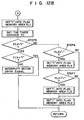
- Figs. 12A and 12B are flow charts showing an index check subroutine for executing a similar motor control attained by the circuit shown in Fig. 9.
- the CPU 100 checks to see if the level of the index output signal from the index sensor 108 is high, that is, if the phototransistor 16T is set nonconductive in STEP 1. If generation of a low- level index output signal from the index sensor 108 is detected, that'is, if the phototransistor 16T is found to be conductive, then the CPU 100 checks to see if the flag memory area FL1 has the content of "1", that is, if the index output signal in the preceding cycle was at a low level in STEP 2.
- the CPU 100 checks to see if the time TL in which the index output signal is kept at a low level is longer than the time TR which is set slightly longer than the time required for one rotation of the floppy disk 6. If TL ⁇ TR, the index check subroutine is ended. If TL > TR, the CPU 100 writes data "0" into each of the flag memory areas FL2 to FL4, interrupts the motor drive signal, and then ends the index check subroutine.
- the CPU 100 checks to see whether or not data "1" has been stored in the flag memory area FL1 in STEP 3.
- the CPU 100 checks to see whether or not data "1" has been stored in the flag memory area FL2 in STEP 4.
- the motor 10 is driven to allow the floppy disk 6 to be rotated, and thereafter, data "0" is stored into the flag memory area FL1.
- data "0" is stored into the flag memory area FL1 without driving the motor 10, thus ending the index check subroutine.
- Fig. 13 shows a subroutine for executing a motor drive signal check.
- the CPU 100 checks to see if the motor drive signal is generated from the control data generator 112 or not. When it is detected that this motor drive signal is not generated, the motor drive signal check subroutine is ended after data "1" has been stored into the flag memory area FL5. On the other hand, when the generation of the motor drive signal is detected, the contents of the flag memory area FL5 is checked. When it is detected that the contents of this flag memory area FL5 is "I”, the motor drive signal check subroutine is ended. When it is detected that the contents of the memory area FL5 is "0", the motor 10 is driven. After data "I" is stored into the flag memory area FL5, the motor drive signal check subroutine is ended.
- the output signal of the index sensor 108 changes from low to high.
- the CPU 100 After the processings in STEPs 1, 3 and 4 were executed, the CPU 100 generates a motor drive signal to drive the motor 10. Due to this, the spindle 8 is rotated and the floppy disk 6 is desirably set on this spindle 8. Data "1" is sequentially stored into the flag memory areas FL2 to FL4 whenever the index hole 6D of this floppy disk 6 is detected by the index sensor 108. In this way, this index hole 6D is detected three times.
- the motor 10 is driven in accordance with the motor drive signal check subroutine. However, the driving of this motor 10 is immediately stopped in accordance with the next index check subroutine. Thereafter the motor 10 is not driven since data "1" has been stored into the flag memory area FL5. Furthermore, in the case where an answer of "NO" is not obtained again in STEP 2 before the time TR elapses after a predetermined time data was set into- the timer counter TC, the CPU 100 will stop the motor 10.
- the present invention has been described above with respect to the embodiments, the invention is not limited to only these embodiments.
- the monostable multivibrator 20, OR gate 26 and initial resetting circuit 30 may be omitted. In this case, even if the motor drive signal MDS is generated when the floppy disk 6 is not inserted, it is possible to inhibit the driving of the motor 10.
Landscapes
- Rotational Drive Of Disk (AREA)
- Indexing, Searching, Synchronizing, And The Amount Of Synchronization Travel Of Record Carriers (AREA)
Applications Claiming Priority (4)
| Application Number | Priority Date | Filing Date | Title |
|---|---|---|---|
| JP74780/83 | 1983-04-27 | ||
| JP74781/83 | 1983-04-27 | ||
| JP7478183A JPS59201270A (ja) | 1983-04-27 | 1983-04-27 | フロツピデイスクドライブ装置 |
| JP7478083A JPS59201269A (ja) | 1983-04-27 | 1983-04-27 | フロツピデイスクドライブ装置 |
Publications (1)
| Publication Number | Publication Date |
|---|---|
| EP0126977A1 true EP0126977A1 (de) | 1984-12-05 |
Family
ID=26415962
Family Applications (1)
| Application Number | Title | Priority Date | Filing Date |
|---|---|---|---|
| EP84104628A Withdrawn EP0126977A1 (de) | 1983-04-27 | 1984-04-25 | Plattenlaufwerk für flexible Platten |
Country Status (2)
| Country | Link |
|---|---|
| US (1) | US4644426A (de) |
| EP (1) | EP0126977A1 (de) |
Cited By (1)
| Publication number | Priority date | Publication date | Assignee | Title |
|---|---|---|---|---|
| GB2256078B (en) * | 1991-05-24 | 1995-04-26 | Samsung Electronics Co Ltd | A circuit for generating a disk change signal |
Families Citing this family (7)
| Publication number | Priority date | Publication date | Assignee | Title |
|---|---|---|---|---|
| US5227927A (en) * | 1986-05-21 | 1993-07-13 | Canon Kabushiki Kaisha | Recording and/or reproducing apparatus adapted to minimized electrical energy consumption |
| JPS63187462A (ja) * | 1987-01-29 | 1988-08-03 | Fujitsu Ltd | 磁気ディスク装置の回転同期制御方式 |
| JPH01194006A (ja) * | 1988-01-29 | 1989-08-04 | Fanuc Ltd | フロッピィディスク駆動用モータの制御装置 |
| JP2836081B2 (ja) * | 1989-01-12 | 1998-12-14 | 日本電気株式会社 | ディスク制御回路 |
| JP3159338B2 (ja) * | 1992-11-17 | 2001-04-23 | ソニー株式会社 | 磁気デイスク装置 |
| WO1996012277A1 (en) * | 1994-10-18 | 1996-04-25 | Iomega Corporation | Disk cartridge detection methods and apparatus |
| US5854719A (en) * | 1994-10-18 | 1998-12-29 | Iomega Corporation | Methods and apparatus for detecting whether a removable cartridge disk drive is empty |
Citations (2)
| Publication number | Priority date | Publication date | Assignee | Title |
|---|---|---|---|---|
| GB2099203A (en) * | 1981-04-28 | 1982-12-01 | Ricoh Kk | Apparatus for driving floppy disc |
| EP0076518A2 (de) * | 1981-10-05 | 1983-04-13 | Hitachi, Ltd. | Speicherplattenwiedergabegerät |
Family Cites Families (9)
| Publication number | Priority date | Publication date | Assignee | Title |
|---|---|---|---|---|
| DE2812574C3 (de) * | 1978-03-22 | 1981-01-29 | Siemens Ag, 1000 Berlin Und 8000 Muenchen | Diskettenlaufwerk |
| US4359763A (en) * | 1979-03-12 | 1982-11-16 | Exxon Research And Engineering Co. | Floppy disc drive |
| US4376293A (en) * | 1979-12-27 | 1983-03-08 | Matsushita Electric Industrial Co., Ltd. | Magnetic disk recording and/or reproducing device |
| JPS5849939B2 (ja) * | 1980-07-29 | 1983-11-08 | 株式会社東芝 | 記録円盤再生装置 |
| US4458273A (en) * | 1981-04-28 | 1984-07-03 | Iomega Corporation | Magnetic disk drive control apparatus and method |
| JPS57212659A (en) * | 1981-06-23 | 1982-12-27 | Ricoh Co Ltd | Floppy disk driving device |
| JPS581856A (ja) * | 1981-06-25 | 1983-01-07 | Ricoh Co Ltd | フロツピ−デイスクドライブ装置 |
| JPS5829177A (ja) * | 1981-08-12 | 1983-02-21 | Toshiba Corp | 磁気デイスク装置の電源供給制御回路 |
| JPS59116959A (ja) * | 1982-12-23 | 1984-07-06 | Canon Inc | 記録又は再生装置 |
-
1984
- 1984-04-19 US US06/602,179 patent/US4644426A/en not_active Expired - Lifetime
- 1984-04-25 EP EP84104628A patent/EP0126977A1/de not_active Withdrawn
Patent Citations (2)
| Publication number | Priority date | Publication date | Assignee | Title |
|---|---|---|---|---|
| GB2099203A (en) * | 1981-04-28 | 1982-12-01 | Ricoh Kk | Apparatus for driving floppy disc |
| EP0076518A2 (de) * | 1981-10-05 | 1983-04-13 | Hitachi, Ltd. | Speicherplattenwiedergabegerät |
Non-Patent Citations (2)
| Title |
|---|
| IBM TECHNICAL DISCLOSURE BULLETIN, vol. 21, no. 2, July 1978, New York, USA; J.F. HOLSTEEN "Head load protect circuit", pages 770-776 * |
| Patent Abstracts of Japan vol. 5, no. 64, 30 April 1981 & JP-A-56 016 960 * |
Cited By (1)
| Publication number | Priority date | Publication date | Assignee | Title |
|---|---|---|---|---|
| GB2256078B (en) * | 1991-05-24 | 1995-04-26 | Samsung Electronics Co Ltd | A circuit for generating a disk change signal |
Also Published As
| Publication number | Publication date |
|---|---|
| US4644426A (en) | 1987-02-17 |
Similar Documents
| Publication | Publication Date | Title |
|---|---|---|
| US5555510A (en) | Automatic computer card insertion and removal algorithm | |
| US5799199A (en) | Memory device in which electrical power consumption of power circuit thereof is reduced during an idle state | |
| US4636905A (en) | Voltage monitoring system for an electric power source of a disc drive | |
| US4644426A (en) | Floppy disk drive apparatus | |
| JPS6363979B2 (de) | ||
| US4563712A (en) | Floppy disk drive apparatus | |
| US4547820A (en) | Floppy disk drive apparatus | |
| US4599659A (en) | Floppy disk drive apparatus | |
| US4686590A (en) | Apparatus for positioning a magnetic head | |
| JPH0731410Y2 (ja) | ディスク装置 | |
| JP2836081B2 (ja) | ディスク制御回路 | |
| US4665445A (en) | Floppy disk drive apparatus | |
| JPH0423342B2 (de) | ||
| JPS61240476A (ja) | 磁気デイスク装置 | |
| KR100205287B1 (ko) | 하드 디스크 드라이브의 액츄에이터 언래칭 감지장치 및 방법 | |
| US6047341A (en) | Disk-cartridge-type adapter including sensor and processor supplying power from power source to drive interface upon detecting rotation of magnet according to sensor output | |
| JPS59127267A (ja) | フロツピデイスクドライブ装置 | |
| EP0133232A1 (de) | Gerät zur Datenübertragung zur Verwendung mit einer flexiblen Magnetplatte und dergleichen | |
| JPH0325341Y2 (de) | ||
| KR860002151B1 (ko) | 양면 플로피 디스크의 삽입시 자동 제어회로 | |
| CN2256556Y (zh) | 硬盘i/o接口卡 | |
| JPS63195860A (ja) | 電子機器 | |
| JPH05325488A (ja) | ディジタルテープカセット及びディジタルデータ記録装置 | |
| JPS638954A (ja) | 不揮発性メモリへの誤書き込み防止装置 | |
| JPS61267121A (ja) | デイスク装置 |
Legal Events
| Date | Code | Title | Description |
|---|---|---|---|
| PUAI | Public reference made under article 153(3) epc to a published international application that has entered the european phase |
Free format text: ORIGINAL CODE: 0009012 |
|
| 17P | Request for examination filed |
Effective date: 19840425 |
|
| AK | Designated contracting states |
Designated state(s): DE FR GB |
|
| 17Q | First examination report despatched |
Effective date: 19861117 |
|
| STAA | Information on the status of an ep patent application or granted ep patent |
Free format text: STATUS: THE APPLICATION IS DEEMED TO BE WITHDRAWN |
|
| 18D | Application deemed to be withdrawn |
Effective date: 19910109 |
|
| RIN1 | Information on inventor provided before grant (corrected) |
Inventor name: SAITO, SHUNJI |