EP0128062A1 - Feldeffekttransistor vom Anreicherungs-Typ - Google Patents
Feldeffekttransistor vom Anreicherungs-Typ Download PDFInfo
- Publication number
- EP0128062A1 EP0128062A1 EP84400902A EP84400902A EP0128062A1 EP 0128062 A1 EP0128062 A1 EP 0128062A1 EP 84400902 A EP84400902 A EP 84400902A EP 84400902 A EP84400902 A EP 84400902A EP 0128062 A1 EP0128062 A1 EP 0128062A1
- Authority
- EP
- European Patent Office
- Prior art keywords
- metallization
- effect transistor
- field effect
- gate
- dielectric layer
- Prior art date
- Legal status (The legal status is an assumption and is not a legal conclusion. Google has not performed a legal analysis and makes no representation as to the accuracy of the status listed.)
- Granted
Links
Images

Classifications
-
- H—ELECTRICITY
- H10—SEMICONDUCTOR DEVICES; ELECTRIC SOLID-STATE DEVICES NOT OTHERWISE PROVIDED FOR
- H10D—INORGANIC ELECTRIC SEMICONDUCTOR DEVICES
- H10D64/00—Electrodes of devices having potential barriers
- H10D64/60—Electrodes characterised by their materials
- H10D64/66—Electrodes having a conductor capacitively coupled to a semiconductor by an insulator, e.g. MIS electrodes
- H10D64/68—Electrodes having a conductor capacitively coupled to a semiconductor by an insulator, e.g. MIS electrodes characterised by the insulator, e.g. by the gate insulator
-
- H—ELECTRICITY
- H10—SEMICONDUCTOR DEVICES; ELECTRIC SOLID-STATE DEVICES NOT OTHERWISE PROVIDED FOR
- H10D—INORGANIC ELECTRIC SEMICONDUCTOR DEVICES
- H10D30/00—Field-effect transistors [FET]
- H10D30/60—Insulated-gate field-effect transistors [IGFET]
- H10D30/67—Thin-film transistors [TFT]
- H10D30/6729—Thin-film transistors [TFT] characterised by the electrodes
- H10D30/6737—Thin-film transistors [TFT] characterised by the electrodes characterised by the electrode materials
- H10D30/6738—Schottky barrier electrodes
-
- H—ELECTRICITY
- H10—SEMICONDUCTOR DEVICES; ELECTRIC SOLID-STATE DEVICES NOT OTHERWISE PROVIDED FOR
- H10D—INORGANIC ELECTRIC SEMICONDUCTOR DEVICES
- H10D30/00—Field-effect transistors [FET]
- H10D30/60—Insulated-gate field-effect transistors [IGFET]
- H10D30/67—Thin-film transistors [TFT]
- H10D30/674—Thin-film transistors [TFT] characterised by the active materials
- H10D30/675—Group III-V materials, Group II-VI materials, Group IV-VI materials, selenium or tellurium
-
- H—ELECTRICITY
- H10—SEMICONDUCTOR DEVICES; ELECTRIC SOLID-STATE DEVICES NOT OTHERWISE PROVIDED FOR
- H10D—INORGANIC ELECTRIC SEMICONDUCTOR DEVICES
- H10D30/00—Field-effect transistors [FET]
- H10D30/80—FETs having rectifying junction gate electrodes
- H10D30/87—FETs having Schottky gate electrodes, e.g. metal-semiconductor FETs [MESFET]
-
- H—ELECTRICITY
- H10—SEMICONDUCTOR DEVICES; ELECTRIC SOLID-STATE DEVICES NOT OTHERWISE PROVIDED FOR
- H10D—INORGANIC ELECTRIC SEMICONDUCTOR DEVICES
- H10D64/00—Electrodes of devices having potential barriers
- H10D64/20—Electrodes characterised by their shapes, relative sizes or dispositions
- H10D64/27—Electrodes not carrying the current to be rectified, amplified, oscillated or switched, e.g. gates
- H10D64/311—Gate electrodes for field-effect devices
- H10D64/411—Gate electrodes for field-effect devices for FETs
-
- H—ELECTRICITY
- H10—SEMICONDUCTOR DEVICES; ELECTRIC SOLID-STATE DEVICES NOT OTHERWISE PROVIDED FOR
- H10D—INORGANIC ELECTRIC SEMICONDUCTOR DEVICES
- H10D64/00—Electrodes of devices having potential barriers
- H10D64/60—Electrodes characterised by their materials
- H10D64/64—Electrodes comprising a Schottky barrier to a semiconductor
-
- H—ELECTRICITY
- H10—SEMICONDUCTOR DEVICES; ELECTRIC SOLID-STATE DEVICES NOT OTHERWISE PROVIDED FOR
- H10D—INORGANIC ELECTRIC SEMICONDUCTOR DEVICES
- H10D62/00—Semiconductor bodies, or regions thereof, of devices having potential barriers
- H10D62/80—Semiconductor bodies, or regions thereof, of devices having potential barriers characterised by the materials
- H10D62/85—Semiconductor bodies, or regions thereof, of devices having potential barriers characterised by the materials being Group III-V materials, e.g. GaAs
Definitions
- the present invention relates to a field effect transistor, operating at microwave frequency, of the enrichment type, in which the control electrode has a metal-insulator-metal structure, according to which the first metal ensures Schottky contact with the active layer of the transistor, the insulator or dielectric has a controlled dielectric leak, and the second metal constitutes the control gate on which the bias voltage is applied.
- the technology of integrated circuits on fast materials such as GaAs in particular mainly uses Schottky gate field effect transistors as active elements.
- the gate consists of a metallization which ensures Schottky contact with the active layer of the transistor on which it is deposited: these transistors are frequently called according to their international designation MESFET, that is to say semiconductor metal transistor.
- MESFETs can work in desertion mode, for which the gate voltage is negative, the space charge zone located under the gate modulating the channel between the transistor access electrodes, the source and the drain. They can also work in a limited enrichment regime: there is a deserted zone for a zero gate voltage, an area which can be reduced by applying a low positive voltage VG on the grid. In fact, this positive voltage is limited by the height of the metal-semiconductor barrier, in the energy diagrams, to a value close to + 0.6 V in practice, voltage beyond which the grid begins to leak in such a way. important.
- MESFET Metal Gate of which is deposited directly on the active layer
- MISFET a transistor according to the known art, the metal grid of which is deposited on an insulating layer itself deposited on the semiconductor material
- MIMFET the transistor according to the invention in which the gate has a metal-insulator-metal structure.
- MESFET type transistors on material such as GaAs, operating in enrichment regime.
- MESFETs have the disadvantage of having a fairly limited current capacity according to the enrichment regime and present the risk of destroying the diode formed by the gate and the active layer, for positive bias voltages.
- MISFET transistor in which an insulating layer separates the gate metallization from the active layer.
- MISFET transistor in which an insulating layer separates the gate metallization from the active layer.
- the distribution of interface states in an MIS or MOS type transistor which is only a particular form of an MIS, does not allow operating under stable bias conditions if the transistor is done on GaAs.
- the grid structure proposed by the invention uses a grid comprising a first metal which forms the Schottky junction with the active layer of the transistor, then a layer of dielectric, that is to say of insulator, having a controlled electrical leak. by construction, during the realization of the transistor, and finally a second metal layer deposited on the dielectric layer, said second metal layer constituting the external electrode, or control gate, on which the bias voltage is applied.
- the leakage in the insulating layer is chosen so that, on the one hand, the Schottky metallization, in contact with the semiconductor material, is maintained in electrical equilibrium with the control grid, or second upper metallization, up to a positive bias voltage close to the conditions of flat bands; and so that, on the other hand, the current in the diode formed by the complex gate and the junction with the active layer of the transistor, is limited for higher bias voltages, thus preserving it from destruction.
- flat bands is meant the conduction and valence bands, in the energy diagrams, these no longer having for certain voltage values such as + 0.6V of barrier between the metal and the semiconductor.
- high bias voltage is meant gate bias voltages greater than 0.6V, since in transistors according to known art the gate begins to leak for voltages of the order of 0.6V, 0.55 to 0.65V depending on achievements.
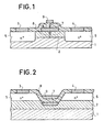
- FIG. 1 represents a simplified diagram, in section, of a MIMFET transistor according to the invention.
- a substrate 1 made of material from the III-V family, but more frequently made of semi-insulating GaAs or InP, supports an active layer 2.
- the transistor has two access electrodes 3 and 4, one of which constitutes the source and the other constitutes the drain of the transistor, these access electrodes being advantageously placed on wells 5 and 6 which limit part of the active layer 2, with a view to decreasing the series source-drain resistance.
- the enrichment transistor according to the invention comprises a control electrode, generally called a gate, which in the present case has a complex structure formed by a first metallization 7, forming Schottky contact with the active layer 2, then by a layer 8 of an insulator having a controlled electrical leak, and finally by a second metallization 9 forming the control grid on which the bias voltage is applied.
- the first metallization 7, the insulator having a leak 8, and the second metallization 9, form a capacitor, and as the dielectric 8 of this capacitor has an electrical leak, the Schottky interface 7 and the control grid 9 are maintained in electrical balance.
- the leakage of the dielectric short-circuits the capacity formed by the two metallizations and the dielectric.
- the transconductance and the pinch voltage are identical to that of an equivalent MESFET, according to known art.
- this type of transistor is designed to work at very high frequencies: at high frequencies, or in dynamic regime, the capacity of the dielectric is in series with the capacity of space charge under the gate, which reduces transconductance and the pinch tension of the channel.
- FIG. 1 are represented the symbolic diagrams of a resistance which represents the controlled leakage of the dielectric layer 8 and of a capacity which represents the capacity of the capacitor formed by the complex metal-insulator-metal grid.
- the space charge under the Schottky grid and the capacity of said space charge are also shown in dotted lines.
- the transistor according to the invention has a theoretical dispersion of its characteristics at low frequencies or at high frequencies, depending on whether the leakage resistance short-circuits a capacitor or whether two capacitors are in series, it is possible to minimize the dispersion of transconductance using as material 8 for the grid a material having a high dielectric constant, preferably between 8 and 30.
- the preferred materials for producing a MIM grid according to the invention are non-stoichiometric oxides of titanium, tantalum or aluminum, for which the dielectric constants are, respectively, of the order of 30, 26 and 12, these may vary depending on the stoichiometry of the oxide.
- Silicon nitride, doped or not with a metal and corresponding to the general formula Si x NyM Z , which has a dielectric constant close to 8 to 10 depending on doping with a metal M is perfectly suitable for producing a MIM grid according to the invention.
- the first metallization 7 is essentially consisting of a metal forming a Schottky contact with the active layer 2: titanium and aluminum, for example, are metals very commonly used for this use.
- the second metallization 9 which essentially constitutes a contact point for bringing a bias to the gate of the transistor must have as a first quality to be well attached to the dielectric layer: it can for example be formed by a series of metallizations titanium, platinum , gold, then recharged with gold if it is necessary to make contact with this control grid 9.
- FIG. 1 represents a MIM field effect transistor according to the invention, produced on materials of the GaAs type and the active layer as well as the wells are of the n type.
- FIG. 2 represents a variant of the transistor according to the invention, and the same reference indices have been kept to designate the same elements in the figure.
- the advantage of this FIG. 2 resides on the one hand in the production of a buried grid, in direct contact with an active layer 2 which is no longer delimited as in FIG. 1 by two boxes 5 and 6.
- This figure shows also that the dielectric layer interposed between the two metal layers 7 and 9 of the gate can advantageously be extended over the entire free access surface of the transistor, and serve as a passivator.
- Figures 3, 4 and 5 compare the drain-source current characteristics I DS as a function of the drain-source voltage V DS for different types of transistors according to the known art and according to the invention.
- the voltage V DS is plotted on the abscissa, at the rate of 0.5 V per division, and the current 1 DS is plotted on the ordinate, at the rate of 5 milliamps per division.
- the different curves correspond to different values of polarization of the grid, these values being reported on the right part of each diagram.
- FIG. 3 represents the normal characteristic curves of a MESFET type field effect transistor. These characteristic curves will serve as benchmarks for Figures 4 and 5.
- FIG. 4 a positive gate voltage is applied to a MESFET type transistor according to the known art.
- the upper curve corresponding to a LV bias voltage of + 1 V, shows a gate leak.
- a more detailed analysis that is to say the analysis of the transistor under tests subjected to gate voltages which no longer proceed in steps of 0.5 V but in steps of 1/10 th of a volt for example, shows that the gate leakage phenomenon appears around + 0.55 V in the case of a MESFET on GaAs.
- FIG. 5 represents the same characteristics for a MIM transistor according to the invention. This figure shows that in the interval between -1 V and + 0.5 V the curves of a transistor according to the invention are exactly identical to the curves of a MESFET transistor according to known art, but that, in addition , the gate bias voltage can be pushed up to + 1.5 V, that is to say almost 3 times the limit value of the transistors of the known art without any gate leakage.
- the operations for manufacturing a MIM transistor according to the invention belong to the knowledge of a person skilled in the art, and are conventional. However, in the case of a transistor having a buried gate as in FIG. 2, the depth of the channel is approximately 400 angstroms.
- the thickness of the insulating layer 8 is of the order of 500 angstroms, and if the silicon nitride rich in silicon, that is to say non stoichiometric, is used to manufacture this layer, it is deposited by plasma and chemical decomposition in vapor phase, by controlling the thickness, close to 500 angstroms, so as to control the current leakage through said dielectric layer, as well as by controlling the possible doping of this layer by a metal since c is the supply of metal which controls the electrical leakage through the layer.
- the transistor according to the invention or MIMFET has transconductance characteristics equivalent to those of a MESFET, but its current transfer capacity, in enrichment, is increased by around 100% compared to that of a conventional MESFET , and the leakage through the gate is suppressed up to gate polarization values of the order of + 1.5 V.
- This MIMFET transistor is essentially used to make logic integrated circuits, preferably on fast materials from group III -V, such as GaAs, Al x Ga lx As, InP, In GaAs but it is conceivable to also use it on silicon although the speed of integrated circuits on silicon is less interesting than that of integrated circuits on GaAs.
Landscapes
- Junction Field-Effect Transistors (AREA)
Applications Claiming Priority (2)
| Application Number | Priority Date | Filing Date | Title |
|---|---|---|---|
| FR8307792 | 1983-05-10 | ||
| FR8307792A FR2545989B1 (fr) | 1983-05-10 | 1983-05-10 | Transistor a effet de champ, fonctionnant en regime d'enrichissement |
Publications (2)
| Publication Number | Publication Date |
|---|---|
| EP0128062A1 true EP0128062A1 (de) | 1984-12-12 |
| EP0128062B1 EP0128062B1 (de) | 1987-02-11 |
Family
ID=9288749
Family Applications (1)
| Application Number | Title | Priority Date | Filing Date |
|---|---|---|---|
| EP84400902A Expired EP0128062B1 (de) | 1983-05-10 | 1984-05-03 | Feldeffekttransistor vom Anreicherungs-Typ |
Country Status (5)
| Country | Link |
|---|---|
| US (1) | US4612560A (de) |
| EP (1) | EP0128062B1 (de) |
| JP (1) | JPS59208880A (de) |
| DE (1) | DE3462381D1 (de) |
| FR (1) | FR2545989B1 (de) |
Families Citing this family (10)
| Publication number | Priority date | Publication date | Assignee | Title |
|---|---|---|---|---|
| JPS60253958A (ja) * | 1984-05-31 | 1985-12-14 | Sharp Corp | センサ |
| EP0226678B1 (de) * | 1985-12-24 | 1989-04-26 | Fujitsu Limited | Logische Schaltung |
| US5027166A (en) * | 1987-12-04 | 1991-06-25 | Sanken Electric Co., Ltd. | High voltage, high speed Schottky semiconductor device and method of fabrication |
| US5688703A (en) * | 1995-09-05 | 1997-11-18 | Motorola, Inc. | Method of manufacturing a gate structure for a metal semiconductor field effect transistor |
| US5882961A (en) * | 1995-09-11 | 1999-03-16 | Motorola, Inc. | Method of manufacturing semiconductor device with reduced charge trapping |
| JP2001127265A (ja) * | 1999-10-29 | 2001-05-11 | Matsushita Electronics Industry Corp | 半導体記憶装置およびその駆動方法 |
| JP2004014547A (ja) * | 2002-06-03 | 2004-01-15 | Toshiba Corp | 半導体装置及び容量調節回路 |
| US8183595B2 (en) * | 2005-07-29 | 2012-05-22 | International Rectifier Corporation | Normally off III-nitride semiconductor device having a programmable gate |
| TWI715018B (zh) | 2018-04-23 | 2021-01-01 | 愛爾蘭商納維達斯半導體有限公司 | 氮化鎵電晶體結構 |
| US20240038869A1 (en) * | 2020-09-18 | 2024-02-01 | Iii-V Technologies Gmbh | Normally-off mesfet device with stacked gate contact |
Citations (1)
| Publication number | Priority date | Publication date | Assignee | Title |
|---|---|---|---|---|
| DE1923279A1 (de) * | 1969-05-07 | 1970-12-23 | Licentia Gmbh | Transistor mit isolierter Steuerelektrode |
Family Cites Families (5)
| Publication number | Priority date | Publication date | Assignee | Title |
|---|---|---|---|---|
| US4016643A (en) * | 1974-10-29 | 1977-04-12 | Raytheon Company | Overlay metallization field effect transistor |
| JPS54127280A (en) * | 1978-03-27 | 1979-10-03 | Sumitomo Electric Ind Ltd | Semiconductor device |
| US4407004A (en) * | 1978-11-13 | 1983-09-27 | Xerox Corporation | Self-aligned MESFET having reduced series resistance |
| US4375643A (en) * | 1980-02-14 | 1983-03-01 | Xerox Corporation | Application of grown oxide bumper insulators to a high-speed VLSI SASMESFET |
| JPS58102565A (ja) * | 1981-12-14 | 1983-06-18 | Fujitsu Ltd | 半導体装置 |
-
1983
- 1983-05-10 FR FR8307792A patent/FR2545989B1/fr not_active Expired
-
1984
- 1984-05-03 EP EP84400902A patent/EP0128062B1/de not_active Expired
- 1984-05-03 DE DE8484400902T patent/DE3462381D1/de not_active Expired
- 1984-05-07 US US06/607,503 patent/US4612560A/en not_active Expired - Fee Related
- 1984-05-09 JP JP59091165A patent/JPS59208880A/ja active Pending
Patent Citations (1)
| Publication number | Priority date | Publication date | Assignee | Title |
|---|---|---|---|---|
| DE1923279A1 (de) * | 1969-05-07 | 1970-12-23 | Licentia Gmbh | Transistor mit isolierter Steuerelektrode |
Non-Patent Citations (6)
| Title |
|---|
| APPLIED PHYSICS LETTERS, vol. 37, no. 1, juillet 1980, pages 61-64, American Institute of Physics, New York, US; D.J. DIMARIA et al.: "Dual electron injector structure" * |
| ELECTRONICS LETTERS, vol. 19, no. 12, juin 1983, pages 434-435, Londres, GB; E. KOHN et al.: "MIM gate FET: new GaAs enhancement-mode transistor" * |
| IBM TECHNICAL DISCLOSURE BULLETIN, vol. 24, no. 5, octobre 1981, page 2452, New York, US; T.L. ANDRADE et al.: "GaAs lossy gate dielectric FET" * |
| IBM TECHNICAL DISCLOSURE BULLETIN, vol. 24, no. 7A, décembre 1981, page 3485, New York, US; J. BOITUZAT et al.: "Characterization method of metalloid contamination in the plasma etching step of Schottky barrier diodes" * |
| JAPANESE JOURNAL OF APPLIED PHYSICS, vol. 21, no. 2, partie 2, février 1982, pages L122-L124, Tokyo, JP; T. HOTTA et al.: "A new AlGaAs/GaAs heterojunction FET with insulated gate structure (MISSFET)" * |
| JOURNAL OF THE ELECTROCHEMICAL SOCIETY, vol. 117, no. 11, novembre 1970, pages 1410-1417; J.E. FOSTER et al.: "Electrical characteristics of the silicon nitride-gallium arsenide interface" * |
Also Published As
| Publication number | Publication date |
|---|---|
| DE3462381D1 (en) | 1987-03-19 |
| JPS59208880A (ja) | 1984-11-27 |
| FR2545989B1 (fr) | 1985-07-05 |
| FR2545989A1 (fr) | 1984-11-16 |
| EP0128062B1 (de) | 1987-02-11 |
| US4612560A (en) | 1986-09-16 |
Similar Documents
| Publication | Publication Date | Title |
|---|---|---|
| EP0543742B1 (de) | Monolithische Niederspannungsschutzdiode mit geringer Kapazität | |
| US5273920A (en) | Method of fabricating a thin film transistor using hydrogen plasma treatment of the gate dielectric/semiconductor layer interface | |
| EP0608376A1 (de) | Spannungsvariabler kondensator | |
| EP0017697A1 (de) | Verbindungsvorrichtung für integrierte Halbleiterschaltungen und Verfahren zu ihrer Herstellung | |
| FR2744836A1 (fr) | Substrat epitaxial a concentration progressive pour dispositif a semi-conducteurs a diffusion par resurf | |
| EP0128062B1 (de) | Feldeffekttransistor vom Anreicherungs-Typ | |
| FR2953995A1 (fr) | Interrupteur de puissance bidirectionnel commandable a la fermeture et a l'ouverture | |
| EP0673068B1 (de) | Schutzeinrichtung gegen Überspannungen in integrierten Schaltungen | |
| FR2843488A1 (fr) | Dispositif de commutation pour un capteur a rayons x | |
| EP0305253B1 (de) | Mikrowellentransistor mit Doppelheteroübergang | |
| FR2694450A1 (fr) | Condensateur en technologie CMOS. | |
| EP0624943B1 (de) | Seriengeschaltetes Strombegrenzerbauelement | |
| EP0011694B1 (de) | Verfahren und Vorrichtung zum reversiblen Einstellen elektrischer Parameter eines Stromkreises | |
| EP4099397A1 (de) | Elektronische vorrichtung mit transistoren | |
| EP3754697A1 (de) | Monolithisches bauteil, das einen leistungstransistor mit galliumnitrid enthält | |
| FR2623017A1 (fr) | Dispositif a semiconducteur organique a base de phtalocyanine | |
| FR2960342A1 (fr) | Commutateur bidirectionnel a commande hf | |
| EP3654384B1 (de) | Halbleitervorrichtung mit feldplatte | |
| EP0128061B1 (de) | Feldeffekttransistor des Verarmungstyps | |
| EP0204387A1 (de) | Halbleiteranordnung zur Herstellung der Entkupplungskapazitäten, die zwischen der Versorgung und der Erdung von integrierten Schaltungen liegen | |
| EP0697734A1 (de) | Schutzschaltung gegen elektrostatische Entladung | |
| EP3648346B1 (de) | Vorspannungsschaltung eines leistungsbauelements | |
| EP0472481B1 (de) | Hochspannungshalbleiteranordnung mit kleinem Leckstrom | |
| FR2574594A1 (fr) | Structure integree de triac a commande par diac | |
| EP0081423B1 (de) | Halbleiteranordnung mit niedriger parasitärer Kapazität mit "beam-lead" Typ Zuleitungen und Verfahren zur Herstellung dieser Anordnung |
Legal Events
| Date | Code | Title | Description |
|---|---|---|---|
| PUAI | Public reference made under article 153(3) epc to a published international application that has entered the european phase |
Free format text: ORIGINAL CODE: 0009012 |
|
| AK | Designated contracting states |
Designated state(s): DE GB NL |
|
| 17P | Request for examination filed |
Effective date: 19841220 |
|
| 17Q | First examination report despatched |
Effective date: 19860415 |
|
| GRAA | (expected) grant |
Free format text: ORIGINAL CODE: 0009210 |
|
| AK | Designated contracting states |
Kind code of ref document: B1 Designated state(s): DE GB NL |
|
| REF | Corresponds to: |
Ref document number: 3462381 Country of ref document: DE Date of ref document: 19870319 |
|
| PLBE | No opposition filed within time limit |
Free format text: ORIGINAL CODE: 0009261 |
|
| STAA | Information on the status of an ep patent application or granted ep patent |
Free format text: STATUS: NO OPPOSITION FILED WITHIN TIME LIMIT |
|
| 26N | No opposition filed | ||
| PGFP | Annual fee paid to national office [announced via postgrant information from national office to epo] |
Ref country code: GB Payment date: 19920427 Year of fee payment: 9 |
|
| PGFP | Annual fee paid to national office [announced via postgrant information from national office to epo] |
Ref country code: DE Payment date: 19920502 Year of fee payment: 9 |
|
| PGFP | Annual fee paid to national office [announced via postgrant information from national office to epo] |
Ref country code: NL Payment date: 19920531 Year of fee payment: 9 |
|
| PG25 | Lapsed in a contracting state [announced via postgrant information from national office to epo] |
Ref country code: GB Effective date: 19930503 |
|
| PG25 | Lapsed in a contracting state [announced via postgrant information from national office to epo] |
Ref country code: NL Effective date: 19931201 |
|
| GBPC | Gb: european patent ceased through non-payment of renewal fee |
Effective date: 19930503 |
|
| NLV4 | Nl: lapsed or anulled due to non-payment of the annual fee | ||
| PG25 | Lapsed in a contracting state [announced via postgrant information from national office to epo] |
Ref country code: DE Effective date: 19940201 |