EP0132415A2 - Drucksystem für einen Punktdrucker - Google Patents
Drucksystem für einen Punktdrucker Download PDFInfo
- Publication number
- EP0132415A2 EP0132415A2 EP84305069A EP84305069A EP0132415A2 EP 0132415 A2 EP0132415 A2 EP 0132415A2 EP 84305069 A EP84305069 A EP 84305069A EP 84305069 A EP84305069 A EP 84305069A EP 0132415 A2 EP0132415 A2 EP 0132415A2
- Authority
- EP
- European Patent Office
- Prior art keywords
- printing
- dot
- data
- pattern
- dots
- Prior art date
- Legal status (The legal status is an assumption and is not a legal conclusion. Google has not performed a legal analysis and makes no representation as to the accuracy of the status listed.)
- Granted
Links
Images





Classifications
-
- G—PHYSICS
- G06—COMPUTING OR CALCULATING; COUNTING
- G06K—GRAPHICAL DATA READING; PRESENTATION OF DATA; RECORD CARRIERS; HANDLING RECORD CARRIERS
- G06K15/00—Arrangements for producing a permanent visual presentation of the output data, e.g. computer output printers
- G06K15/02—Arrangements for producing a permanent visual presentation of the output data, e.g. computer output printers using printers
- G06K15/10—Arrangements for producing a permanent visual presentation of the output data, e.g. computer output printers using printers by matrix printers
-
- G—PHYSICS
- G06—COMPUTING OR CALCULATING; COUNTING
- G06K—GRAPHICAL DATA READING; PRESENTATION OF DATA; RECORD CARRIERS; HANDLING RECORD CARRIERS
- G06K2215/00—Arrangements for producing a permanent visual presentation of the output data
- G06K2215/111—Arrangements for producing a permanent visual presentation of the output data with overlapping swaths
Definitions
- the present invention relates to a printing system for performing high-grade printing in a dot printer in which letters or symbols are printed by aggregated dots.
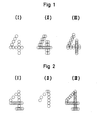
- Fig. 1-(I) shows a basic dot pattern
- Figs. 1-(II) and 1-(III) show a high-grade printing pattern
- Figs. 2-(I) and 2-(II) show two different printing patterns
- Fig. 2-(III) shows the high-grade printing pattern.
- numeral 4 is used as an example of the pattern.
- a first conventional system the number of wires of a printing head is increased and dots are arranged in zigzags to form a high-density dot arrangement.
- This system is defective in that, though the required high-grade printing can be attained, the structure and control of the apparatus are complicated and the apparatus is expensive.
- a basic pattern as shown in Fig. 1-(I) is slightly shifted in the horizontal direction as shown in F ig. 1-(II) and printing is then carried out again.
- the basic pattern is slightly shifted in the vertical direction as shown in Fig. 1-(III) and printing is carried out again.
- the operation is simple and the apparatus is not expensive.
- the system is defective in that the quality of printed letters is poor.
- the present invention relates to a printing system in which a second dot matrix pattern is generated from a basic dot matrix pattern by an algorithm so that gaps between desirable dots of the basic dot matrix pattern are filled up, and the basic dot matrix pattern and the second dot matrix pattern are synthesized to obtain printing of the synthesized dot matrix pattern.
- the claimed system is advantageous in that a high-grade printing pattern can be obtained with a simple apparatus without increasing the number of wires of a printing head.
- a further advantage is that the required memory capacity is reduced relative to where printing is carried out two times while slightly shifting different printing patterns.
- Fig. 3 is a block diagram illustrating the structure of an apparatus according to one embodiment of the present invention.
- Reference numeral 10 represents a microprocessor (hereinafter referred to as "CPU") for controlling a printer
- reference numeral 12 represents a read-only memory (hereinafter referred to as "ROMa”) for storing a program therein.
- Reference numeral 14 represents a read-only memory (hereinafter referred to as "ROMb”) for storing a dot pattern of letters or symbols therein and reference numeral 16 represents an I/O driver driven by instructions from CPU 10.
- a printing head 18 is connected to the I/O driver 16.
- An LF motor (not shown) for effecting line shifting in a printing paper, a spacing SP motor (not shown) for moving the printing head 18 in the printing direction and an interface portion (not shown) for taking in printing data are connected to the I/O driver 16.
- the respective parts are connected to one another through bus lines 20.
- CPU 10 receives control data and printing data from the interface according to the program stored in ROMa 12. On receipt of the printing data, a letter dot pattern is read out from ROMb 14 by using the received data as an address.
- the control data indicates high-grade printing
- the letter dot pattern read out from ROMb 14 is edited according to a conversion algorithm and printing is carried out based on the edited data.
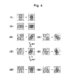
- Figs. 4-(I) through 4-(IIX) show algorithmic conversion of various basic patterns.
- Dot 0 indicates data of the dot read out from ROMb 14, indicates the absence of data read out from ROMb 14 on the corresponding bit, and indicates data of the dot to be interpolated.
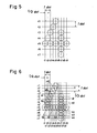
- Fig. 5 shows a basic pattern which is read out from ROMb 14.
- the basic pattern is a letter pattern consisting of 7 vertical rows (r l through r 7 ) and 9 horizontal columns (c l through cg).
- Fig. 6 shows a printing pattern formed by printing a second pattern edited according to the conversion algorithm shown in Fig. 4 on the basic pattern shown in Fig. 5.
- Fig. 6 al through a4 indicate interpolated dots according to the conversion shown in Fig. 4-(I)
- bl through b4 indicate interpolated dots according to the conversion shown in Fig. 4-(II)
- el through e3 indicate interpolated dots according to the conversion shown in Fig. 4-(V)
- hl indicates an interpolated dot according to the conversion shown in Fig. 4-(IIX).
- Printing of this numeral 4 is performed by the printing head 18 shown in Fig. 3.
- This printing head 18 comprises seven wires, and at the first spacing (one pass), dots of rows rl through r7 shown in Fig. 6 are printed, and a printing paper is shifted upward by 1/2 dot or the printing head 18 is shifted downward by 1/2 dot.
- dots r 1 ' through r 6 ' shown in Fig. 6 are printed to effect high-grade printing as shown in F ig. 6.
- Printing for filling up gaps in the basic pattern is performed based on the interpolation data according to the conversion algorithm.
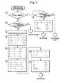
- Fig. 7 is a flow chart illustrating the conversion procesing using integer columns
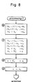
- Fig. 8 is a flow chart illustrating the conversion processing using columns other than integer columns.
- c l through cg shown in Fig. 6 are used as the integer columns, and R n , R n-1 and Rn+1 represent registers for storing printing data of the column to be printed, printing data of the preceding column and printing data of the next column, respectively.
- R n , R n-1 and R n +l represent registers for storing printing data of the column appearing 1/4 dot after the column to be printed, printing data of the column appearing 1/4 dot before the column to be printed and printing data of the column appearing 3/4 dot after the column to be printed respectively.
- Each of R a through R d and R x through R z represents a general-purpose register, Rx represents a register for storing printing data appearing 1/4 dot before the column to be printed, and A represents an accumulator.
- Rx represents a register for storing printing data appearing 1/4 dot before the column to be printed
- A represents an accumulator.
- " . " indicates a logical product
- + " indicates a logical sum
- " x2 " represents 1-bit shift-up " - " indicates a complement
- " xl/2 " indicates 1-bit shift-down.
- Reference numerals 1through 13 are step numbers.
- the SP motor in Fig. 3 is driven to move the printing head 18 to a predetermined position, and a letter code to be printed is given to CPU 10 from the interface through the I/O driver.
- CPU 10 reads out the printing data of the column to be printed and the next column from ROMb 14 and these data are stored in the registers R n and R n+1 . At this point, 0 is stored in the register R n-1 .
- the conversion processing shown in Fig. 7 is started. At first, it is judged at the step 1 whether or not it is the first pass. If it is judged that the pass is the first pass, the step 2is carried out and the interpolation shown in Fig. 4-(II) is carried out.
- ROMb 14 reads out the subsequent printing data and stores it in the register R n+1 .
- printing is started by giving the data of the accumulator A to the printing head 18.
- the printing operation is transferred to the subsequent integer column, and in this manner, the steps 1and 2 are repeated to complete printing of one letter.
- CPU 10 receives the next letter code and the above steps are repeated.
- printing of one line is carried out. This corresponds to the state where printing of the rows r l through r 7 is conducted over one line.
- the printing paper is shifted upward by 1/2 dot or the printing head 18 is shifted downward by 1/2 dot, and the printing head 18 is returned to the position of the first letter to be printed on the new line and printing of the second pass is started.
- the printing data are stored in the registers R n , Rn - 1 and R n+1 .
- the flow enters into the step 3 from the step 1.
- the step 3 it is judged whether or not the column is an integer column, and when it is judged that the column is an integer column, the flow enters into the step
- the processing of forming the interpolation data shown in fig. 4-(I) is carried out, and at the step 5 , the processing of forming the interpolation data shown in Figs. 4-(I I I) and 4-(IV) is carried out. Only when there is no data on the bit in Figs. 4-(III) and 4-(IV), at the step 6 , the interpolation data obtained at the step 5 is effectively processed.
- the processing for effecting the interpolation shown in Figs. 4-(VII) and 4-(IIX) is performed (the processing for interpolating a dot at the median when three dots form a triangle).
- the editing processing is carried out so that printing is not effected on the row where printing has been effected before 1/4 dot.
- the processing for preparing for printing of the next column is carried out at the step 9.
- the foregoing processing is one using integer columns, as shown in Fig. 7, and the conversion processing columns other than the integer columns, as shown in Fig. 8, is further carried out.
- the processing for forming the interpolation data shown in Figs. 4-(V) and 4-(VI) is carried out. Only when there is no data on the bit in Figs. 4-(V) and 4-(VI), at the step 11, the processing for rendering the interpolationdata obtained at the step 10 effective is carried out.
- the same editing processing as conducted at the step .8 shown in Fig. 7 is carried out at the step @, and the preparatory processing as conducted at the step 9shown in Fig. 7 is carried out at the step 13.
- This printing of the second pass is accomplished by giving the data obtained by the editing processing conducted at the step 8 and the data of the accumulator A obtained at the step 12 to the printing head 18.
- step 3 When printing of one column is completed, printing of the next column is started and step 3 and subsequent steps are repeated, until printing of one letter is completed.
- This operation corresponds to printing of the rows r l ' through r 6 ' shown in Fig. 6.
- CPU 10 receives the letter code of the subsequent letter and the above-mentioned steps are repeated. In this manner, printing of one line is completed. This corresponds to the state where printing is effected over 1 line with respect to the rows r 1 ' through r 6 ' shown in Fig. 6. Printing of letters of this line according to the algorithmic conversion processing, that is, high-grade printing, is thus completed.
- the conversion processing is carried out at a low printing speed of the printer.
- a buffer memory is connected to the bus line 20 shown in Fig. 3, and the editing processing is carried out before the printing operation to store printing data in the buffer memory.
- the printing data is read out from the buffer memory and printing is then performed. If this arrangement is adopted, the above-mentioned effects can similarly be attained even if the printing speed is high.
- the results of editing at the step 2 shown in Fig. 7 and the results of editing at the steps 8O and 12shown in Figs. 7 and 8 are separately stored in the buffer memory, and other procedures are the same as in the above-mentioned embodiment and the printing data of the first pass and the printing data of the second pass are read out from the separated areas of the buffer memory, respectively.
- the dot matrix has been described with reference to the dot matrix having 7 rows and 9 columns, but the dot matrix is not limited to this dot matrix.
- it can be carried out on any basic dot matrix irrespective of the dot matrix structure and a dot pattern of high-grade printing can be obtained with a reduced memory capacity.
- the number of letters used for an ordinary printer is about 256 inclusive of alphabetic letters, numerical letters, symbols and kana letters.
- a conversion program of about 200 bytes is sufficient.
- the present invention will now be described with reference to a second embodiment where the printing density is doubled in the column direction, that is, printing is carried out at 1/2 dot intervals to further increase the printing grade.
- interpolation in the column direction need not be computed.
- the data of the basic pattern and the auxiliary data of dots to be interpolated are stored in the ROMb 14 shown in Fig. 3, as shown in Fig. 12-(II) (pattern A is illustrated as an example).
- Fig. 12-(I) shows the memory space
- a 1 , A 2 , .... A 17 represent addresses and bl , b2 whil b8 represent bits of each address.
- a 1 , A 2 , .... A 17 are made to correspond to columns C 1 , C2, .... C17 shown in Fig. 10-(I) and the bits b 1 , b 2 , .... b 7 are made to correspond to rows r l , r 2 , .... r 7 .
- the memory space has a 8-bit width, though the width of the memory space is not limited to this width.
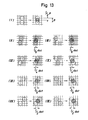
- Fig. 13 diagrammatically shows the conversion algorithm of the present embodiment.
- Fig. 10-(I) one letter is horizontally divided into segments of 1/4 dot, but the interval between two continuous dots in the horizontal direction is 1/2 dot and there is no continuity of the interval of 1/4 dot. The reason is that since the interval of 1/2 dot is sufficient for the printing grade in the horizontal direction and the printing speed of the printer is limited by the repeated driving speed of the printing head, the dot interval in the horizontal direction cannot be so narrowed for increasing the printing speed.
- the auxiliary data 1 for determining whether or not the interpolation dot should be added can be added relatively to the printing data as shown in Fig. 12-(II). Addition of the auxiliary data 1 may be accomplished by adding data "1" of the subsequent dot positions of the same row to the positions of two basic dots where interpolation is not desired.
- auxiliary data 1 is added to the position of (A 6 , b 4 ) subsequent to the position of address A5 and b i t 4 corresponding to dot D [hereinafter referred to as " ( A5 , b4 )"; similar abbreviations will be used hereinafter] and the position of (A 7 , b 5 ) subsequent to the position of ( A6 , b 5 ) corresponding to dot E.
- auxiliary data 1 s added to the position of ( A14 , b 4 ) and the position of ( A 13 , b 5 ). In this case, the reading direction is of A 1 ⁇ A 17 .
- the following method is adopted for forming the printing data for the above printing operation.
- the data of address A 1 [hereinafter referred to as “ ( A 1 ) "; similar abbreviations will be used with reference to A 2 , A 3 , ....] is directly used in the column C 1 , and with respect to the column C 3 (stored at address A 2 ), logical product (A 1 ).
- (A 2 ) of the preceding printing data (A 1 ) and the present printing data ( A2 ) is computed and by inversion (A 1 ).(A 2 ) of this logical operation, the position of the auxiliary data-stored bit (the data at this position is logic " 0 ”) is known. Furthermore, the logic product (A 1 ). (A 2 ).
- (A 2 ) of the obtained result and the present printing data ( A2 ) is computed to obtain the data to be practically printed.
- the data to be practically printed that is, [ (A 1 ). (A 2 ). (A 2 ) ] . (A 3 ). (A 3 ), is similarly determined from the preceding printing data [ (A 1 ).(A 2 ).(A 2 ) ] and the present printing data (A3).
- the columns C 7 , C 9 , .... C 33 data to be practically printed will similarly be obtained.
- the printing data is logic " 0 ".
- the pattern to be printed in this case is as shown in Fig. 10-(I) and the interval between two continuous dots is 1/2 dot or more, as pointed out hereinbefore.
- the printing paper is shifted upward by 1/2 pitch (1/2P) and interpolation dots are printed while setting the driving timing of the printing head at 1/8 dot.
- the column where the auxiliary data (left “ ⁇ ") corresponding to the printing data of the column Y 0 is carried is designated as Y l
- the printing data of the column Y 1 is designated as R 1 .
- the column where the auxiliary data (right “ ⁇ ”) corresponding to the printing data of the column Y2 is carried is designated as Y 3
- the printing data of the column Y3 is designated as R 3 .
- the columns Y 1 , Y 2 , and Y3 are located at the odd number column positions shown in Fig. 10(11), and the printing data and auxiliary data are stored in the letter pattern-storing memory as shown in Fig. 12(11).
- Formation of the interpolation dot data is accomplished according to the following procedures.
- R 2' is a value obtained by shifting R2 by 1 bit in the direction of a solid line arrow and mark " . " indicates a logical product.
- R 0 ' is a value obtained by shifting R 0 by 1 bit in the direction of a solid line arrow.
- (R 0 ⁇ R 1 ) and (R 2 .R 3 ) are formulas for determining the auxiliary data
- data " 1 " is auxiliary data (the printing data is not continuous between the columns Y o and Y 1 or between the columns Y 2 and Y 3 ).
- (R 2 .R 3 )' is a value obtained by shifting the result (R 2 ⁇ R 3 ) of the logical operation by 1 bit in the direction of a dotted line arrow.
- (R 0 ⁇ R 1 )' is a value obtained by shifting the result (R 0 ⁇ R 1 ) by 1 bit in the direction of a dotted line arrow.
- the data of the interpolation dot to be practically printed is determined from the stipulation data obtained in the methods (i) and (ii) and the interpolation-inhibiting data obtained in the methods (iii) and (iv) according to the following logical operation:
- " + " represents the logical sum.
- the data to be printed is determined from the above formula (5) and (6) as follows: i
- the dot to be printed at this time is dot in Fig. 10-(II), and the interval between two continuous dots in the horizontal direction is 1/2 dot or more.
- a second matrix pattern is generated from a basic dot matrix pattern by the algorithmic conversion processing, and both the dot matrix patterns are synthesized and edited so that gaps of the basic dot matrix pattern are filled up, whereby the following effects are attained.
- the memory capacity can be reduced, as compared with the conventional system where printing is carried out while slightly shifting different patterns.
- the described system is advantageous over the conventional system where the wire number is increased, because the structure of the apparatus can be simplified and the cost of the apparatus can be reduced.
- the capacity of the letter pattern-storing memory for high-grade printing can be reduced, and the logical operation for determining the interpolation dot is simplified and the printing grade is further enhanced.
Landscapes
- Physics & Mathematics (AREA)
- Engineering & Computer Science (AREA)
- Mathematical Physics (AREA)
- General Engineering & Computer Science (AREA)
- General Physics & Mathematics (AREA)
- Theoretical Computer Science (AREA)
- Dot-Matrix Printers And Others (AREA)
Applications Claiming Priority (4)
| Application Number | Priority Date | Filing Date | Title |
|---|---|---|---|
| JP135228/83 | 1983-07-26 | ||
| JP13522883A JPS6027552A (ja) | 1983-07-26 | 1983-07-26 | ドツトプリンタの印字方式 |
| JP17316383A JPS6064858A (ja) | 1983-09-21 | 1983-09-21 | ドットプリンタの文字パターン作成方法 |
| JP173163/83 | 1983-09-21 |
Publications (3)
| Publication Number | Publication Date |
|---|---|
| EP0132415A2 true EP0132415A2 (de) | 1985-01-30 |
| EP0132415A3 EP0132415A3 (en) | 1985-10-09 |
| EP0132415B1 EP0132415B1 (de) | 1988-11-02 |
Family
ID=26469124
Family Applications (1)
| Application Number | Title | Priority Date | Filing Date |
|---|---|---|---|
| EP84305069A Expired EP0132415B1 (de) | 1983-07-26 | 1984-07-25 | Drucksystem für einen Punktdrucker |
Country Status (3)
| Country | Link |
|---|---|
| US (1) | US4632579A (de) |
| EP (1) | EP0132415B1 (de) |
| DE (1) | DE3474933D1 (de) |
Cited By (5)
| Publication number | Priority date | Publication date | Assignee | Title |
|---|---|---|---|---|
| EP0159895A3 (en) * | 1984-04-20 | 1986-05-28 | International Business Machines Corporation | Printer for printing characters in two alternative print qualities |
| US4652155A (en) * | 1984-06-18 | 1987-03-24 | Hitachi, Ltd. | Printer having a thermal head |
| GB2199967A (en) * | 1987-01-13 | 1988-07-20 | Plessey Co Plc | Character enhancement systems |
| EP0526738A3 (en) * | 1991-07-05 | 1993-08-11 | Oki Electric Industry Co., Ltd. | Printer having print data correction circuit |
| EP0207788B1 (de) * | 1985-07-03 | 1993-09-01 | Lexmark International, Inc. | Gerät und Verfahren zur Aufzeichnung von Punktmatrix Zeichen in hervorgehobener Form |
Families Citing this family (16)
| Publication number | Priority date | Publication date | Assignee | Title |
|---|---|---|---|---|
| JP2835719B2 (ja) * | 1986-07-14 | 1998-12-14 | 株式会社日立製作所 | 画像処理装置 |
| US4851825A (en) * | 1987-07-24 | 1989-07-25 | Naiman Abraham C | Grayscale character generator and method |
| JPH0832469B2 (ja) * | 1988-01-29 | 1996-03-29 | 富士通株式会社 | ビットマップフォントの横拡大方式 |
| DE68927008T2 (de) * | 1988-09-26 | 1997-03-20 | Oki Electric Ind Co Ltd | Verfahren zum komprimieren und dekomprimieren von punktmatrixzeichen |
| US5016195A (en) * | 1989-03-03 | 1991-05-14 | Da Vinci Graphics, Inc. | High quality plotting technique for raster printing devices |
| JPH02232690A (ja) * | 1989-03-04 | 1990-09-14 | Brother Ind Ltd | データ変換装置 |
| US5239312A (en) * | 1990-02-02 | 1993-08-24 | Dataproducts Corporation | Interlaced ink jet printing |
| US5070345A (en) * | 1990-02-02 | 1991-12-03 | Dataproducts Corporation | Interlaced ink jet printing |
| JP2647226B2 (ja) * | 1990-03-23 | 1997-08-27 | 沖電気工業株式会社 | ドットパターン圧縮方法及び伸長方法 |
| US5410615A (en) * | 1990-09-25 | 1995-04-25 | Xerox Corporation | Bitmap image resolution converter compensating for write-white xerographic laser printing |
| US5282057A (en) * | 1990-04-23 | 1994-01-25 | Xerox Corporation | Bit-map image resolution converter |
| US5555557A (en) * | 1990-04-23 | 1996-09-10 | Xerox Corporation | Bit-map image resolution converter with controlled compensation for write-white xerographic laser printing |
| US5480240A (en) * | 1993-12-01 | 1996-01-02 | Lexmark International, Inc. | Print quality enhancement method and apparatus |
| GB9819081D0 (en) * | 1998-09-03 | 1998-10-28 | Videojet Systems Int | An ink jet printing system |
| JP3520034B2 (ja) * | 2000-07-25 | 2004-04-19 | 古河電気工業株式会社 | 電子電気機器部品用銅合金材 |
| CN113689334B (zh) * | 2021-08-24 | 2024-12-03 | 深圳市先地图像科技有限公司 | 一种激光成像设备以及激光成像控制方法 |
Family Cites Families (3)
| Publication number | Priority date | Publication date | Assignee | Title |
|---|---|---|---|---|
| US4242003A (en) * | 1978-10-16 | 1980-12-30 | Xerox Corporation | Multi-pass matrix printing |
| JPS5738165A (en) * | 1980-08-18 | 1982-03-02 | Seiko Epson Corp | Serial dot printer |
| US4584573A (en) * | 1981-07-20 | 1986-04-22 | Sharp Kabushiki Kaisha | Combined character and background pattern print control system |
-
1984
- 1984-07-25 DE DE8484305069T patent/DE3474933D1/de not_active Expired
- 1984-07-25 EP EP84305069A patent/EP0132415B1/de not_active Expired
-
1985
- 1985-12-26 US US06/815,280 patent/US4632579A/en not_active Expired - Lifetime
Cited By (9)
| Publication number | Priority date | Publication date | Assignee | Title |
|---|---|---|---|---|
| EP0159895A3 (en) * | 1984-04-20 | 1986-05-28 | International Business Machines Corporation | Printer for printing characters in two alternative print qualities |
| US4652155A (en) * | 1984-06-18 | 1987-03-24 | Hitachi, Ltd. | Printer having a thermal head |
| EP0207788B1 (de) * | 1985-07-03 | 1993-09-01 | Lexmark International, Inc. | Gerät und Verfahren zur Aufzeichnung von Punktmatrix Zeichen in hervorgehobener Form |
| GB2199967A (en) * | 1987-01-13 | 1988-07-20 | Plessey Co Plc | Character enhancement systems |
| GB2199967B (en) * | 1987-01-13 | 1990-12-05 | Plessey Co Plc | Improvements in or relating to character enhancement systems |
| EP0526738A3 (en) * | 1991-07-05 | 1993-08-11 | Oki Electric Industry Co., Ltd. | Printer having print data correction circuit |
| EP0744707A3 (de) * | 1991-07-05 | 1997-10-01 | Oki Electric Ind Co Ltd | Drucker mit einer Druckdatenverbesserungsschaltung |
| US6049349A (en) * | 1991-07-05 | 2000-04-11 | Oki Electric Industry Co., Ltd. | Printer having print data correction circuit |
| US6373513B1 (en) | 1991-07-05 | 2002-04-16 | Oki Data Corporation | Printer having print data correction circuit |
Also Published As
| Publication number | Publication date |
|---|---|
| DE3474933D1 (en) | 1988-12-08 |
| EP0132415B1 (de) | 1988-11-02 |
| US4632579A (en) | 1986-12-30 |
| EP0132415A3 (en) | 1985-10-09 |
Similar Documents
| Publication | Publication Date | Title |
|---|---|---|
| EP0132415B1 (de) | Drucksystem für einen Punktdrucker | |
| US4400791A (en) | Dot matrix printer with compressed character data storage | |
| US5207517A (en) | Methods of compression and expansion of dot pattern | |
| EP0159895B1 (de) | Drucker zum Drucken von Zeichen in zwei alternativen Druckqualitäten | |
| EP0326295B1 (de) | Verfahren zum Vergrössern der Daten eines Bitrasters in einer horizontalen Richtung | |
| EP0436026B1 (de) | Verfahren zum komprimieren und dekomprimieren von punktmatrixzeichen | |
| GB2243808A (en) | Deriving draft quality dot patterns from letter quality dot patterns in matrix printers | |
| CA1108303A (en) | Method and apparatus for addressing a character generator | |
| JP2000158720A (ja) | バーコード印刷装置 | |
| EP0114989B1 (de) | Thermischer Druckerund Verfahren zum thermischen Drucken | |
| JPH0795392A (ja) | ファクシミリ画像の平滑化スケーリング方法 | |
| EP0009662A2 (de) | Verfahren und Vorrichtung zum Speichern und Darstellen von Zeichen, die der chinesischen Schrift ähnlich sind | |
| JPH0457510B2 (de) | ||
| WO1988001571A1 (en) | Dot matrix printer | |
| JPH0632953B2 (ja) | ドットプリンタの印字方法 | |
| EP0542316B1 (de) | Vorrichtung zur Erzeugung von Bit-Map-Daten | |
| JPH0358310B2 (de) | ||
| JPH021677B2 (de) | ||
| JPH0525673B2 (de) | ||
| KR910009064B1 (ko) | 프린터용 문자크기의 보정방법 | |
| JP3003266B2 (ja) | シリアルプリンタ | |
| JPH03120060A (ja) | 縮小印刷方法 | |
| JPS62290546A (ja) | 記録装置 | |
| JPH05246075A (ja) | ビットマップデ−タ発生装置 | |
| JPH0419167A (ja) | 印字装置 |
Legal Events
| Date | Code | Title | Description |
|---|---|---|---|
| PUAI | Public reference made under article 153(3) epc to a published international application that has entered the european phase |
Free format text: ORIGINAL CODE: 0009012 |
|
| AK | Designated contracting states |
Designated state(s): DE FR GB |
|
| 17P | Request for examination filed |
Effective date: 19841220 |
|
| PUAL | Search report despatched |
Free format text: ORIGINAL CODE: 0009013 |
|
| AK | Designated contracting states |
Designated state(s): DE FR GB |
|
| 17Q | First examination report despatched |
Effective date: 19870129 |
|
| GRAA | (expected) grant |
Free format text: ORIGINAL CODE: 0009210 |
|
| AK | Designated contracting states |
Kind code of ref document: B1 Designated state(s): DE FR GB |
|
| ET | Fr: translation filed | ||
| REF | Corresponds to: |
Ref document number: 3474933 Country of ref document: DE Date of ref document: 19881208 |
|
| PLBE | No opposition filed within time limit |
Free format text: ORIGINAL CODE: 0009261 |
|
| STAA | Information on the status of an ep patent application or granted ep patent |
Free format text: STATUS: NO OPPOSITION FILED WITHIN TIME LIMIT |
|
| 26N | No opposition filed | ||
| PGFP | Annual fee paid to national office [announced via postgrant information from national office to epo] |
Ref country code: FR Payment date: 19980709 Year of fee payment: 15 |
|
| PGFP | Annual fee paid to national office [announced via postgrant information from national office to epo] |
Ref country code: GB Payment date: 19980716 Year of fee payment: 15 |
|
| PGFP | Annual fee paid to national office [announced via postgrant information from national office to epo] |
Ref country code: DE Payment date: 19980803 Year of fee payment: 15 |
|
| PG25 | Lapsed in a contracting state [announced via postgrant information from national office to epo] |
Ref country code: GB Free format text: LAPSE BECAUSE OF NON-PAYMENT OF DUE FEES Effective date: 19990725 |
|
| PG25 | Lapsed in a contracting state [announced via postgrant information from national office to epo] |
Ref country code: FR Free format text: THE PATENT HAS BEEN ANNULLED BY A DECISION OF A NATIONAL AUTHORITY Effective date: 19990731 |
|
| GBPC | Gb: european patent ceased through non-payment of renewal fee |
Effective date: 19990725 |
|
| PG25 | Lapsed in a contracting state [announced via postgrant information from national office to epo] |
Ref country code: DE Free format text: LAPSE BECAUSE OF NON-PAYMENT OF DUE FEES Effective date: 20000503 |
|
| REG | Reference to a national code |
Ref country code: FR Ref legal event code: ST |