EP0132849A2 - Bekleidete metallische Leiterrahmen-Substrate - Google Patents
Bekleidete metallische Leiterrahmen-Substrate Download PDFInfo
- Publication number
- EP0132849A2 EP0132849A2 EP84108887A EP84108887A EP0132849A2 EP 0132849 A2 EP0132849 A2 EP 0132849A2 EP 84108887 A EP84108887 A EP 84108887A EP 84108887 A EP84108887 A EP 84108887A EP 0132849 A2 EP0132849 A2 EP 0132849A2
- Authority
- EP
- European Patent Office
- Prior art keywords
- cladding
- composite structure
- substrate
- nickel
- lead frame
- Prior art date
- Legal status (The legal status is an assumption and is not a legal conclusion. Google has not performed a legal analysis and makes no representation as to the accuracy of the status listed.)
- Withdrawn
Links
Images
Classifications
-
- H—ELECTRICITY
- H10—SEMICONDUCTOR DEVICES; ELECTRIC SOLID-STATE DEVICES NOT OTHERWISE PROVIDED FOR
- H10W—GENERIC PACKAGES, INTERCONNECTIONS, CONNECTORS OR OTHER CONSTRUCTIONAL DETAILS OF DEVICES COVERED BY CLASS H10
- H10W76/00—Containers; Fillings or auxiliary members therefor; Seals
- H10W76/10—Containers or parts thereof
- H10W76/12—Containers or parts thereof characterised by their shape
- H10W76/15—Containers comprising an insulating or insulated base
- H10W76/157—Containers comprising an insulating or insulated base having interconnections parallel to the insulating or insulated base
-
- H—ELECTRICITY
- H10—SEMICONDUCTOR DEVICES; ELECTRIC SOLID-STATE DEVICES NOT OTHERWISE PROVIDED FOR
- H10W—GENERIC PACKAGES, INTERCONNECTIONS, CONNECTORS OR OTHER CONSTRUCTIONAL DETAILS OF DEVICES COVERED BY CLASS H10
- H10W70/00—Package substrates; Interposers; Redistribution layers [RDL]
- H10W70/40—Leadframes
- H10W70/456—Materials
- H10W70/457—Materials of metallic layers on leadframes
-
- H—ELECTRICITY
- H10—SEMICONDUCTOR DEVICES; ELECTRIC SOLID-STATE DEVICES NOT OTHERWISE PROVIDED FOR
- H10W—GENERIC PACKAGES, INTERCONNECTIONS, CONNECTORS OR OTHER CONSTRUCTIONAL DETAILS OF DEVICES COVERED BY CLASS H10
- H10W72/00—Interconnections or connectors in packages
- H10W72/50—Bond wires
- H10W72/551—Materials of bond wires
- H10W72/552—Materials of bond wires comprising metals or metalloids, e.g. silver
- H10W72/5522—Materials of bond wires comprising metals or metalloids, e.g. silver comprising gold [Au]
-
- H—ELECTRICITY
- H10—SEMICONDUCTOR DEVICES; ELECTRIC SOLID-STATE DEVICES NOT OTHERWISE PROVIDED FOR
- H10W—GENERIC PACKAGES, INTERCONNECTIONS, CONNECTORS OR OTHER CONSTRUCTIONAL DETAILS OF DEVICES COVERED BY CLASS H10
- H10W72/00—Interconnections or connectors in packages
- H10W72/50—Bond wires
- H10W72/551—Materials of bond wires
- H10W72/552—Materials of bond wires comprising metals or metalloids, e.g. silver
- H10W72/5524—Materials of bond wires comprising metals or metalloids, e.g. silver comprising aluminium [Al]
-
- H—ELECTRICITY
- H10—SEMICONDUCTOR DEVICES; ELECTRIC SOLID-STATE DEVICES NOT OTHERWISE PROVIDED FOR
- H10W—GENERIC PACKAGES, INTERCONNECTIONS, CONNECTORS OR OTHER CONSTRUCTIONAL DETAILS OF DEVICES COVERED BY CLASS H10
- H10W72/00—Interconnections or connectors in packages
- H10W72/851—Dispositions of multiple connectors or interconnections
- H10W72/874—On different surfaces
- H10W72/884—Die-attach connectors and bond wires
-
- H—ELECTRICITY
- H10—SEMICONDUCTOR DEVICES; ELECTRIC SOLID-STATE DEVICES NOT OTHERWISE PROVIDED FOR
- H10W—GENERIC PACKAGES, INTERCONNECTIONS, CONNECTORS OR OTHER CONSTRUCTIONAL DETAILS OF DEVICES COVERED BY CLASS H10
- H10W90/00—Package configurations
- H10W90/701—Package configurations characterised by the relative positions of pads or connectors relative to package parts
- H10W90/751—Package configurations characterised by the relative positions of pads or connectors relative to package parts of bond wires
- H10W90/756—Package configurations characterised by the relative positions of pads or connectors relative to package parts of bond wires between a chip and a stacked lead frame, conducting package substrate or heat sink
Definitions
- CRDIP ceramic dual-in-line integrated circuit packages
- a suitable glass is applied to an aluminum-oxide-ceramic substrate using any desired technique such as silk screening.
- the glass is then fused into a homogeneous glass layer which adheres to the aluminum-oxide-ceramic substrate.
- a lead frame is partially embedded into a glass layer.
- a semiconductor chip is affixed to the surface of the substrate by any conventional technique including a gold-silicon eutectic brazing, a lead-base soldering, a glass soldering, or applying a high temperature adhesive.
- An alternative CERDIP package uses a lead frame having a pad incorporated therein.
- the chip is affixed to the lead frame by any suitable mounting means such as solder.
- lead wires are interconnected between the bonding pads on the chip and the lead frame.
- a preglazed ceramic substrate and preglazed ceramic cover are. simultaneously disposed on either side of the lead frame and fused together with glass. The chip is then suspended in the space between the substrate and cover attached to the alumina substrate as described with regards to the previous CERDIP package.
- the fundamental design of the CERDIP package is controlled by several factors such as those which follow.
- the aluminum-oxide-ceramic material used to form the substrate and cover has a relatively low coefficient of thermal expansion.
- the metal lead frame having a substantially higher coefficeint of thermal expansion is bonded to the ceramic, the resulting mismatch in the thermal expansion coefficients can cause stress failures when a wide operational temperature range is encountered.
- This problem has been partially bypassed by designing the lead frame of iron-nickel alloys which have a coefficient of thermal expansion that is relatively close to that of the aluminum-oxide-ceramic. This approach does effectively reduce stress failures between the lead frame and the surrounding ceramic. However, it does create several additional problems which must be overcome.
- the lead wire between the chip and the lead frame can be quickly and easily bonded to both the aluminum metallization or pad on the - semiconductor chip and onto the lead frame.
- gold wire is customarily used because of its fast bonding speed.
- the sealing temperature of between about 400 and 450°C required for glass sealing would quickly form gold-aluminum lead wire. Even if the temperature could be reduced to around 200°C, gold-aluminum intermetallics would form and result in a high risk of CERDIP failure at the brittle bond.
- the electronics industry has overcome this problem by bonding aluminum lead wires to the aluminum metallized pad on the chip and onto the lead frame.
- ultrasonic bonding generally requires a long process time to attach the aluminum lead wire to the chip and the lead frame.
- the time factor results in the use of aluminum wire being more expensive than the use of gold wire.
- nickel-iron base alloys Another consideration in the use of nickel-iron base alloys is the need to place an aluminum pad on the alloy to which the aluminum lead wire can be bonded.
- the electronics industry commonly provides an aluminum stripe on at least one surface of a nickel-iron alloy core to which the aluminum lead wire is bonded.
- the stripe may be produced either by vapor deposition or by cladding.
- One serious disadvantage of the aluminum striped nickel-iron alloy is that the temperature required to anneal and soften the nickel-iron alloy would melt the aluminum stripe.
- the maximum amount of cold work which can be tolerated by the nickel-iron core is limited by the need to subsequentially form or bend the lead frame without fracture. This problem may actually be exacerbated by the processing requirements that the CERDIP lead frames be finally bent along an axis parallel to the direction of rolling.
- the resulting cold work tolerance requires the bonding of the aluminum to the nickel-iron alloy to be performed at thicknesses only moderately above the final thickness, i.e. about .010 in. and the aluminum feed stock to be very thin, i.e. less than about .001 in. which creates handling problems.
- Another disadvantage of aluminum striped nickel-iron alloy is the difficulty in applying solder to these bare nickel-iron alloy portions of the lead frame which were subjected to glass sealing temperatures. Accordingly, it is difficult to attach the completed CERDIP package device to a printed circuit board.
- the assembly includes a lead frame formed from a composite structure.
- the composite structure comprises a substrate formed of a nickel-iron alloy.
- a cladding is bonded to opposite surfaces of the substrate.
- the cladding consists essentially of about 15% to about 70% nickel and the balance essentially copper.
- a second embodiment of the integrated circuit assembly also relates to a lead frame formed from a composite structure.
- the composite structure comprises a substrate formed of a nickel-iron alloy.
- a cladding material is bonded to. opposite surfaces of the substrate for providing the lead frame with relatively high electrical and thermal conductivity.
- a second cladding material bonded to opposite surfaces of the first cladding so that the lead frame has a coefficient of thermal expansion of between 50 to about 100 x 10 -7 in/in/°C.
- a third cladding of aluminum is bonded to opposite surfaces of the second cladding to enhance the bondability of the lead frame to an aluminum lead wire.
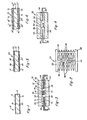
- the composite structure 10 characterized by a relatively low coefficient of thermal expansion.
- the composite comprises a substrate 12 formed of a nickel-iron alloy. Claddings 14 and l6 are bonded to opposite surfaces 18 and 20 of the substrate 12.
- the cladding is an alloy consisting of about 15 to 70% nickel and the balance essentially copper.
- the composite structure has a coefficient of thermal expansion between about 50 x 10 -7 to about 100 x 10 -7 in/in/°C in the temperature range of about 30 to about 450°C.
- the substrate 12 of the composite structure 10 is a nickel-iron alloy which the electronics industry has found to be particularly useful as lead frame material for CERDIP packages.
- the iron-nickel alloy exhibits excellent mechanical properties, including high yield and tensile strengths, high modulus of elasticity and excellent elongation characteristics.
- the alloy composition is in the range of about 35% nickel and the balance essentially iron to about 45% nickel and the balance essentially iron.
- the coefficient of thermal expansion of these alloys is below about 71 x 10 -7 in/in/°C.
- nickel-64 iron commonly called INVAR
- 42 nickel-58 iron commonly known as 42 nickel alloy
- 42 nickel alloy has a coefficient of thermal expansion of about 71 x 10 -7 in/in/°C within the temperature range of about 30 to about 450 C.
- a phase transformation of the alloy occurs so that it may be unsuitable for incorporation as lead frame material into CERDIP packages.
- nickel-iron alloys are of primary interest in the present invention, it is also within the terms of the present invention to form the substrate 12 from other alloys such as an iron-nickel-cobalt alloy which maintains its coefficient of thermal expansion over a wider range of temperature.
- alloy of this type is 29% nickel, 70% cobalt, and the balance essentially iron.
- This latter configuration has a coefficient of thermal expansion of about 53 x 10 -7 in/in/°C in the temperature range of about 30 to about 450 C.
- alloys having a coefficient of thermal expansion in this range frequently are a source of failures of CERDIP packages being subjected to high temperature cycling.
- the cause of the failure is the mismatch in thermal expansion coefficient between the substrate metal and the glass seal and/or alumina base and cover.
- the typical aluminum striped nickel-iron lead frame can tolerate only a minimum amount of annealing and cold work.
- a cladding 14 and 16 is bonded to opposite surfaces 18 and 20, respectively, of the substrate 12.
- the cladding is an alloy consisting essentially of about l5 to about 70% nickel and the balance essentially copper. A more preferred range of the alloy is about 15 to about 40% nickel and the balance essentially copper. A most preferred range of the alloy is about 20 to about 30% nickel and the balance essentially copper.
- One or more additional elements may be present in the alloys provided they do not interfere with the role of the nickel addition and do not adversely'affect other desirable properties.
- the elements which may be added include zinc, manganese, iron, tin, chromium and molybdenum.
- These elements may be present in the following levels: up to about 25% zinc; up to about 6% manganese; up to about 1% iron; up to about 1% tin; up to about 3% chromium; and up to about 2% molybdenum. These elements may be chosen to further resist the formation of copper-aluminum intermetallics. As used herein, the percentages described are weight percentages.
- the copper-nickel alloy is advantageous to the present invention because of its ability to retard the growth of copper-aluminum intermetallics. In the applications suggested for the present invention, substantial copper-aluminum intermetallics would cause brittle bonds between the aluminum lead wire and the. lead frame and ultimately failure of the electronic package.
- the coefficient - of thermal expansion of these alloys is in the range of about 150 x 10 -7 to about 170 x 10 -7 in/in/°C in the temperature range of about 30 to about 450°C.
- the cladding is applied onto the substrate so that the coefficient of thermal expansion of the resulting composite is between about 50 x 10 -7 to about 100 x 10 7 in/in/°C in the temperature range of about 30 to about 450°C.
- each layer of cladding 14 and 16 may comprise between about 5 to about 20% of the thickness of the total composite structure.
- the composite metal laminate material is used in integrated circuit assemblies, such as lead frames, the material may have a thickness of about .010 inches.
- the present invention may provide the composite with any desired thickness.
- the thickness of cladding depends upon the desired coefficient of thermal expansion of the substrate. For example, if the substrate were formed of INVAR, the cladding would be thicker than if the substrate were formed with 42 nickel.
- Each of the clad layers must be of substantially the same thickness to prevent thermostatic deflection during temperature cycling.
- the cladding may be applied using any conventional technique such as, for example, the bonding principle as disclosed in U.S. Patent No, 3,381,364.
- the bonding can be accomplished using a substrate and cladding layers of substantial thickness followed by rolling and heat treatment to obtain the desired hardness.
- the annealing or heat treating temperature is between about 850°C to about 1000°C.
- the melting temperature of the nickel-copper is about 1170°C and the melting temperature of the nickel-iron is about 1450°C, there are no special process problems in annealing the composite. By contrast, this anneal cannot be performed with a conventional aluminum striped nickel-iron alloy because the aluminum has a melting temperature of about 600°C.
- the composite structure 10 is particularly useful when incorporated into an integrated circuit assembly 22 of the type shown in Figure 3.
- the circuit assembly may include a lead frame 24 formed of the composite 10 which may be of any conventional configuration such as shown in Figure 2.
- the specific design of the lead frame is not a part of the present invention.
- the lead frame configuration shown in Figure 2 includes support rails 26 and 28 and side bars 30 and 32. After the lead frame is sealed into the integrated circuit assembly 22, illustrated as a CERDIP package therein, the rails and side bars are removed as will'be explained hereinbelow.
- the integrated circuit assembly 22 is preferably a conventional CERDIP package including an aluminum-oxide-ceramic substrate 34 and and aluminum-oxide-ceramic cover 36.
- a glass or ceramic 38 bonds the substrate 34 to the cover 36 so as to hermetically seal integrated circuit chip 40 within an enclosed space 42.
- the glass or ceramic preferably has a low melting temperature and a coefficient of thermal expansion in the range of about 50 x 10 -7 to about 100 x 10 7 in/in/°C in the temperature range of about 30 .to about 450°C. More specifically, the glass is a low melting temperature lead-oxide base glass having a melting temperature in the range of about 350 to about 460°C.
- the glass may include additives to. adjust the coefficient of thermal expansion to the individual applications as required. Table I lists various exemplary glasses which are adapted for use in accordance with this invention.
- a lead frame of the type illustrated in Figure 2 and similar to those commonly used in plastic dual-in-line packages is incorporated.
- the lead frame 24 is formed from a composite structure of materials in accordance with the description of the composite structure 10.
- the chip 40 is mounted on the pad 44 by a conventional bonding means such as a gold-silicon eutectic braze, a lead base soldering operation, a glass soldering operation, or application of a high temperature adhesive.
- bonding pads 46 (usually aluminized) on chip 40 are conneccted to the appropriate lead tips 48 with lead wires 50.
- the lead wires are preferably of aluminum wire and may be bonded to the pads 46 and the outermost layer 51 using a conventional technique such as ultrasonic bonding. Then, a preglazed pair of ceramic or glass components 38 of the type described above are placed between the ceramic substrate and ceramic cover 36 and fused into place. Since the melting temperature of the glass is relatively low, and the package has a relatively brief exposure time of less than about 10 minutes and preferably less than 8 minutes at about 400°C, the integrated circuit chip is not adversely effected and intermetallics formed between the aluminum and the copper-nickel base cladding are insufficient to degrade the bond performance.
- the thermal dissipation characteristics of the package illustrated in Figure 3 are somewhat inferior to those of the more conventional CERDIP packages of the type shown in Figure 4. This is because the chip is suspended in space rather than attached to the moderately conductive alumina substrate. With certain devices and applications, substantial thermal dissipation is not required and, therefore, the thermal dissipation characteristics of this package may be quite acceptable.
- the primary advantage of the type of package as shown in Figure 3 is the reduction in processing steps as compared with the number of steps required for more conventional CERDIP package of Figure 4. The reduction in processing steps provides a significant lowering of-manufacturing costs.
- the package of Figure 3 with an aluminum striped nickel-iron alloy lead frame first required the removal of the aluminum cladding from the area of the lead frame to which the chip was bonded. This step was necessary because of the inability to practically solder or braze to aluminum. Next, this area required electroplating with a metal such as silver or gold in order to solder or braze the chip in place since even the solderability of the nickel-iron is poor. Both of these operations are relatively expensive and their cost has generally inhibited the wide spread use of this package.
- the copper-nickel alloy cladding of the nickel-iron alloy as taught by the present invention eliminates the need to remove the cladding or to plate the area to which the chip is to be bonded since the copper-nickel itself is solderable.
- CERDIP package 52 includes an aluminum-oxide-ceramic substrate 34 and cover 36.
- a glass or ceramic 38 seals the cover to the substrate.
- a conventional lead frame 53 formed of a unique composite, as described in the present invention, is connected to chip 40 by lead wires 50.
- glass or ceramic 38 is applied to the aluminum-oxide-ceramic substrate 34 by any conventional technique such as silk screening. Then-, the glass is fused into a homogeneous glass layer adherent to the ceramic substrate. Either separately or concurrently with the glass fusing step, a lead frame 53 is partially embedded in the glass layer.
- a semiconductor chip 40 is affixed to the surface of the substrate by any conventional handling technique such as gold-silicon eutectic brazing, lead base soldering, glass soldering or applying a high temperature adhesive. Then, aluminum lead wires are ultrasonically bonded to bonding pads 46 on the chip 40 and to the tips 48 of the lead frame in order to electrically interconnect the chip to the lead frame.
- a cover 36 having a layer of glass 38 fused thereon, as described with regards to substrate 34, is then positioned above the substrate and heated to fuse the two layers of glass together and hermetically seal chip 40 within the package 52.
- FIG. 5 there is illustrated a composite structure 60 characterized by a relatively low coefficient of thermal expansion and a relatively high thermal comductivity.
- the composite is similar to composite 10 of Figure 1 and identical elements are designated by primed numerals.
- the composite comprises a substrate 12' which is a nickel-iron alloy of the type described with regards to the composite structure 10 described hereinabove.
- Cladding layers 62 and 64 are bonded to opposite surfaces 18' and 20' of substrate 12'.
- the cladding layers consist of a copper or copper alloy having a conductivity of between about 113 to about 226 B.T.U./ft 2 /ft/hr/°F and a preferred range of about 172 to about 226 B.T.U./ft 2 /ft/hr/ o F.
- cladding layers 14' and 16' are bonded to the surfaces 66 and 68 of the cladding layers 62 and 64, respectively.
- outer claddings 14' and 16' are essentially identical with the cladding layers 14 and 16 of the composite 10. and consist essentialy of about 20 to about 70% nickel and the balance essentially copper.
- the thickness of the claddings are determined so that composite structure 60 has a coefficient of thermal expansion of between 50 x 10 -7 to about 100 x 10 -7 in/in/°C at a temperature range of about 30 to about 450°C and a thermal conductivity of between about 30 to about 75 B.T.U./ft 2 /ft/hr/°F.
- the cladding layers 62, 64, 14' and l6' may be applied using any conventional technique such as the bonding principle of U.S. Patent No. 3,381,364.
- Each layer of copper-nickel alloy cladding 14' and 16' may comprise about 5 to about 10% of the thickness of the total composite structure and each layer of copper or copper alloy cladding 62 and 64 may comprise about 20 to about 40% of the thickness of the total composite structure.
- a lower expansivity material such as 36 nickel-54 iron may be used for the substrate 12' in order to obtain the desired coefficient of thermal expansion of the composite.
- the clad layers of a particular material must be of substantially the same thickness to prevent thermostatic deflection during temperature cycling. For instance, the thickness of cladding layers 62 and 64 must be substantially the same and the thickness of'claddings 1 4 ' and l6' must be substantially the same.
- the composite structure 60 is particularly useful when incorporated as a lead frame into an integrated circuit assembly of the type shown in Figures 3 and 4.
- the laminated composite 60 may be formed into a lead frame of any desired configuration and substituted for lead frames 24 or 53 in Figures 3 and 4, respectively.
- the cladding layers 62 and 64 provide a highly conductive path for heat dissipation from the inside of the circuit assemblies 22 and 52 to the atmosphere or to a connected heat sink (not shown).
- Composite 70 which is also characterized by a relatively low coefficient of thermal expansion and a relatively high thermal conductivity.
- the composite 70 is similar to the composites 10 and 60 of Figures 1 and 5, respectively, and similar components are designated by double primed numbers.
- Composite 70 comprises a substrate 12" formed of a nickel-iron alloy. Cladding layers 62" and 64" are bonded to surfaces 18" and 20" of substrate 12". Layers 62" and 64" are formed of a copper or copper alloy having a thermal conductivity of about 113 to about 226 B.T.U./ft 2 /ft/hr/°F as further elaborated hereinabove.
- Second cladding layers 14" and 16" consist essentially of about 20 to about 70% nickel and the balance essentially copper and are bonded to opposite surfaces 66" and 68" of the first cladding layers 62" and 64", respectively, to insure that the composite structure has a coefficient of thermal expansion in the range of about 50 to about 100 in/in/°C at a temperature range of about 30 to 450°C and a thermal conductivity of between about 30 to about 75 B.T.U./ft 2 /ft/hr/°F.
- third cladding layers 72 and 74 are bonded to opposite surfaces 76 and 78 of the second cladding layers 14" and 16", respectively.
- the third cladding layers are formed of aluminum or aluminum alloy and may enhance the wire bonding of aluminum wire to its surface in specified applications of the type described hereinbelow.
- the claddings 72 and 74 comprise aluminum foil.
- the cladding layers 62", 64", 14", 16", 72 and 74 may be bonded by using any conventional technique such as the banding procedure of U.S. Patent No. 3,381,364 set forth hereinabove.
- Each layer of the copper-nickel alloy cladding l4" and 16" may comprise about 5 to about 10% of the thickness of the total composite structure.
- Each layer of copper or copper alloy cladding 62" and 64" may comprise about 20 to about 40% of the thickness of the total composite structure.
- each layer of the aluminum or aluminum alloy cladding 72 and 74 may comprise about 1 to about 3% of the total composite thickness.
- a lower expandivity material such as the 36 nickel-54 iron may be used for the substrate 12", in order to obtain the desired coefficient of thermal expansion of the composite.
- The'clad layers of each particular material must be substantially the same thickness to prevent thermostatic deflection during temperature cycling. For instance, the thickness of cladding layers 62" and 64" must be substantially the same and the thickness of cladding layers 14" and l6" must be substantially the same. Finally, the thickness of cladding layers 72 and 74 must also be substantially the same.
- the composite structure 70 is particularly useful when incorporated into an integrated circuit assembly of the type shown in Figures 3 and 4.
- the composite may be formed into lead frames 24 or 53 having any conventional configuration such as the design illustrated in Figure 2.
- the integrated circuit assemblies combined with the lead frame formed of the composite 70 may be particularly useful to improve the relatively poor solderability of the commonly employed nickel-iron alloys and to simultaneously provide improved thermal and electrical conductivities in conjunction therewith.
- the aluminum lead wires 50 may be conveniently bonded using techniques such as ultrasonic bonding to the aluminum cladding layers 72 or 74.
- the lead frame has a coefficient of thermal expansion of between about 50 to about 100 in/in/°C in a temperature range of about 30 to 450°C and a thermal conductivity of between about 30 to about 75 B.T.U./ft 2 /ft/hr/°F.
- the coefficient of thermal expansion prevents stress failure from mismatch in the thermal expansion coefficient between the lead frame, the alumina cover and base and the glass or ceramic seal.
- the thermal conductivity dissipates the heat generated within the package.
- the ends of the lead frame which are external to the package are generally soldered to some other device such as, for example, a printed circuit board. Since the outer aluminum cladding does not easily solder, it is convenient to remove the aluminum cladding external to the package. This may be accomplished by masking the area or areas of the cladding which it is desired to retain and removing the aluminum by etching from the areas where it is not wanted. It is also within the scope of the present invention to remove the aluminum cladding using any other desired technique.
Landscapes
- Lead Frames For Integrated Circuits (AREA)
Applications Claiming Priority (2)
| Application Number | Priority Date | Filing Date | Title |
|---|---|---|---|
| US07/517,592 US5001546A (en) | 1983-07-27 | 1983-07-27 | Clad metal lead frame substrates |
| US517592 | 1983-07-27 |
Publications (2)
| Publication Number | Publication Date |
|---|---|
| EP0132849A2 true EP0132849A2 (de) | 1985-02-13 |
| EP0132849A3 EP0132849A3 (de) | 1986-11-26 |
Family
ID=24060428
Family Applications (1)
| Application Number | Title | Priority Date | Filing Date |
|---|---|---|---|
| EP84108887A Withdrawn EP0132849A3 (de) | 1983-07-27 | 1984-07-26 | Bekleidete metallische Leiterrahmen-Substrate |
Country Status (3)
| Country | Link |
|---|---|
| US (1) | US5001546A (de) |
| EP (1) | EP0132849A3 (de) |
| JP (1) | JPS6043851A (de) |
Cited By (3)
| Publication number | Priority date | Publication date | Assignee | Title |
|---|---|---|---|---|
| GB2285883A (en) * | 1994-01-13 | 1995-07-26 | Samsung Electronics Co Ltd | Lead frame for semiconductor device |
| CN101847615A (zh) * | 2010-05-12 | 2010-09-29 | 北京中庆微数字设备开发有限公司 | 集成电路芯片封装体 |
| CN119208153A (zh) * | 2024-09-23 | 2024-12-27 | 泰州东田电子有限公司 | 一种半导体封装用高散热引线框架及其制作方法 |
Families Citing this family (36)
| Publication number | Priority date | Publication date | Assignee | Title |
|---|---|---|---|---|
| US5066614A (en) * | 1988-11-21 | 1991-11-19 | Honeywell Inc. | Method of manufacturing a leadframe having conductive elements preformed with solder bumps |
| US5161729A (en) * | 1988-11-21 | 1992-11-10 | Honeywell Inc. | Package to semiconductor chip active interconnect site method |
| US5015803A (en) * | 1989-05-31 | 1991-05-14 | Olin Corporation | Thermal performance package for integrated circuit chip |
| JP2736453B2 (ja) * | 1989-11-27 | 1998-04-02 | 京セラ株式会社 | 半導体素子収納用パッケージ |
| JP2736452B2 (ja) * | 1989-11-27 | 1998-04-02 | 京セラ株式会社 | 半導体素子収納用パッケージ |
| JP2736460B2 (ja) * | 1989-11-30 | 1998-04-02 | 京セラ株式会社 | 半導体素子収納用パッケージ |
| US5300809A (en) * | 1989-12-12 | 1994-04-05 | Sumitomo Special Metals Co., Ltd. | Heat-conductive composite material |
| EP0434264B1 (de) * | 1989-12-22 | 1994-10-12 | Westinghouse Electric Corporation | Gehäuse für Leistungshalbleiterbauelemente |
| US5453293A (en) * | 1991-07-17 | 1995-09-26 | Beane; Alan F. | Methods of manufacturing coated particles having desired values of intrinsic properties and methods of applying the coated particles to objects |
| US5820721A (en) * | 1991-07-17 | 1998-10-13 | Beane; Alan F. | Manufacturing particles and articles having engineered properties |
| US5343073A (en) * | 1992-01-17 | 1994-08-30 | Olin Corporation | Lead frames having a chromium and zinc alloy coating |
| US5608267A (en) * | 1992-09-17 | 1997-03-04 | Olin Corporation | Molded plastic semiconductor package including heat spreader |
| US5540378A (en) * | 1993-09-27 | 1996-07-30 | Olin Corporation | Method for the assembly of an electronic package |
| US5728285A (en) * | 1993-12-27 | 1998-03-17 | National Semiconductor Corporation | Protective coating combination for lead frames |
| US5650661A (en) * | 1993-12-27 | 1997-07-22 | National Semiconductor Corporation | Protective coating combination for lead frames |
| KR970010678B1 (ko) * | 1994-03-30 | 1997-06-30 | 엘지반도체 주식회사 | 리드 프레임 및 이를 이용한 반도체 패키지 |
| US5661336A (en) * | 1994-05-03 | 1997-08-26 | Phelps, Jr.; Douglas Wallace | Tape application platform and processes therefor |
| US5969414A (en) * | 1994-05-25 | 1999-10-19 | Advanced Technology Interconnect Incorporated | Semiconductor package with molded plastic body |
| US5573845A (en) * | 1994-12-09 | 1996-11-12 | Olin Corporation | Superficial coating layer having acicular structures for electrical conductors |
| US5545850A (en) * | 1995-01-13 | 1996-08-13 | Olin Corporation | Guard ring for integrated circuit package |
| US5744752A (en) * | 1995-06-05 | 1998-04-28 | International Business Machines Corporation | Hermetic thin film metallized sealband for SCM and MCM-D modules |
| KR19990028818A (ko) * | 1995-07-14 | 1999-04-15 | 와인스타인 폴 | 금속 볼 그리드 전자 패키지 |
| US5916695A (en) * | 1995-12-18 | 1999-06-29 | Olin Corporation | Tin coated electrical connector |
| KR0183645B1 (ko) * | 1996-03-26 | 1999-03-20 | 이대원 | 다층 구조의 도금층을 구비한 반도체 리드 프레임 |
| JP3259894B2 (ja) * | 1996-04-30 | 2002-02-25 | ソニー株式会社 | リードフレーム、その製造方法及びそのリードフレームを用いた半導体装置 |
| KR100231828B1 (ko) * | 1997-02-20 | 1999-12-01 | 유무성 | 다층 도금 리드프레임 |
| US6037653A (en) * | 1997-03-25 | 2000-03-14 | Samsung Aerospace Industries, Ltd. | Semiconductor lead frame having multi-layered plating layer including copper-nickel plating layer |
| US6083633A (en) * | 1997-06-16 | 2000-07-04 | Olin Corporation | Multi-layer diffusion barrier for a tin coated electrical connector |
| US5809663A (en) * | 1997-07-17 | 1998-09-22 | Perque; Allen J. | Portable, solar powered clothes dryer |
| US6255723B1 (en) * | 1997-10-27 | 2001-07-03 | Tessera, Inc. | Layered lead structures |
| TW446627B (en) * | 1998-09-30 | 2001-07-21 | Toyo Kohan Co Ltd | A clad sheet for lead frame, a lead frame using thereof and a manufacturing method thereof |
| US6545342B1 (en) * | 1999-05-03 | 2003-04-08 | Texas Instruments Incorporated | Pre-finished leadframe for semiconductor devices and method of fabrication |
| US20030137032A1 (en) * | 2000-05-01 | 2003-07-24 | Abbott Donald C. | Pre-finished leadframe for semiconductor devices and method fo fabrication |
| US6759142B2 (en) | 2001-07-31 | 2004-07-06 | Kobe Steel Ltd. | Plated copper alloy material and process for production thereof |
| JP5578326B2 (ja) * | 2011-03-29 | 2014-08-27 | 日立金属株式会社 | リード部品及びその製造方法、並びに半導体パッケージ |
| KR102335720B1 (ko) * | 2017-03-27 | 2021-12-07 | 삼성전자주식회사 | 표면 실장용 금속 유닛 및 이를 포함하는 전자 장치 |
Family Cites Families (19)
| Publication number | Priority date | Publication date | Assignee | Title |
|---|---|---|---|---|
| CA913812A (en) * | 1972-10-31 | The Jade Corporation | Method of forming leads for attachment to semi-conductor devices | |
| US3381364A (en) * | 1965-05-07 | 1968-05-07 | Olin Mathieson | Process for obtaining a clad article with a copper base alloy core |
| US3568301A (en) * | 1968-03-30 | 1971-03-09 | Chugai Electric Ind Co Ltd | Bonding of precious metal to a metal substrate and product therefor |
| US3684464A (en) * | 1970-11-04 | 1972-08-15 | Texas Instruments Inc | Composite metal laminate material and lead frame |
| US3689684A (en) * | 1971-02-05 | 1972-09-05 | Du Pont | Lead frame connector and electronic packages containing same |
| US3832769A (en) * | 1971-05-26 | 1974-09-03 | Minnesota Mining & Mfg | Circuitry and method |
| JPS5151281A (de) * | 1974-10-31 | 1976-05-06 | Tokyo Shibaura Electric Co | |
| US3999955A (en) * | 1975-07-15 | 1976-12-28 | Allegheny Ludlum Industries, Inc. | Strip for lead frames |
| US4055062A (en) * | 1975-07-15 | 1977-10-25 | Allegheny Ludlum Industries, Inc. | Process for manufacturing strip lead frames |
| JPS52116074A (en) * | 1976-03-26 | 1977-09-29 | Hitachi Ltd | Electronic part |
| US4071909A (en) * | 1976-09-30 | 1978-01-31 | Xerox Corporation | Digital interface system for a printer |
| JPS5596665A (en) * | 1979-01-19 | 1980-07-23 | Totoku Electric Co Ltd | Lead component for semiconductor element |
| JPS5690546A (en) * | 1979-12-24 | 1981-07-22 | Sumitomo Electric Ind Ltd | Composite material for semiconductor part |
| JPS5727051A (en) * | 1980-07-25 | 1982-02-13 | Nippon Telegr & Teleph Corp <Ntt> | Copper nickel tin alloy for integrated circuit conductor and its manufacture |
| JPS5817649A (ja) * | 1981-07-24 | 1983-02-01 | Fujitsu Ltd | 電子部品パツケ−ジ |
| US4500028A (en) * | 1982-06-28 | 1985-02-19 | Olin Corporation | Method of forming a composite material having improved bond strength |
| JPS5936952A (ja) * | 1982-08-25 | 1984-02-29 | Toshiba Corp | 半導体装置 |
| US4498121A (en) * | 1983-01-13 | 1985-02-05 | Olin Corporation | Copper alloys for suppressing growth of Cu-Al intermetallic compounds |
| US4441118A (en) * | 1983-01-13 | 1984-04-03 | Olin Corporation | Composite copper nickel alloys with improved solderability shelf life |
-
1983
- 1983-07-27 US US07/517,592 patent/US5001546A/en not_active Expired - Fee Related
-
1984
- 1984-07-26 JP JP59154156A patent/JPS6043851A/ja active Pending
- 1984-07-26 EP EP84108887A patent/EP0132849A3/de not_active Withdrawn
Cited By (5)
| Publication number | Priority date | Publication date | Assignee | Title |
|---|---|---|---|---|
| GB2285883A (en) * | 1994-01-13 | 1995-07-26 | Samsung Electronics Co Ltd | Lead frame for semiconductor device |
| GB2285883B (en) * | 1994-01-13 | 1998-01-21 | Samsung Electronics Co Ltd | Lead frame for semiconductor devices |
| CN101847615A (zh) * | 2010-05-12 | 2010-09-29 | 北京中庆微数字设备开发有限公司 | 集成电路芯片封装体 |
| CN101847615B (zh) * | 2010-05-12 | 2016-02-03 | 北京中庆微数字设备开发有限公司 | 集成电路芯片封装体 |
| CN119208153A (zh) * | 2024-09-23 | 2024-12-27 | 泰州东田电子有限公司 | 一种半导体封装用高散热引线框架及其制作方法 |
Also Published As
| Publication number | Publication date |
|---|---|
| US5001546A (en) | 1991-03-19 |
| JPS6043851A (ja) | 1985-03-08 |
| EP0132849A3 (de) | 1986-11-26 |
Similar Documents
| Publication | Publication Date | Title |
|---|---|---|
| US5001546A (en) | Clad metal lead frame substrates | |
| US4656499A (en) | Hermetically sealed semiconductor casing | |
| US4784974A (en) | Method of making a hermetically sealed semiconductor casing | |
| US4542259A (en) | High density packages | |
| US4577056A (en) | Hermetically sealed metal package | |
| US4524238A (en) | Semiconductor packages | |
| US4556899A (en) | Insulated type semiconductor devices | |
| US5506446A (en) | Electronic package having improved wire bonding capability | |
| US5889320A (en) | Tape application platform and processes therefor | |
| US4682414A (en) | Multi-layer circuitry | |
| US4827377A (en) | Multi-layer circuitry | |
| JPH04162756A (ja) | 半導体モジュール | |
| US4649229A (en) | All metal flat package for microcircuitry | |
| JPS6318648A (ja) | 窒化アルミニウム回路基板 | |
| CA1201211A (en) | Hermetically sealed semiconductor casing | |
| Smith et al. | Hybrid Microcircuit Tape Chip Carrier Materials/Processing Trade-Offs | |
| JP3199018B2 (ja) | 光モジュール | |
| JP2521624Y2 (ja) | 半導体装置 | |
| JP2614495B2 (ja) | 電子部品搭載用基板 | |
| JPH01273690A (ja) | ロウ付け用材料 | |
| JPS5835956A (ja) | 混成集積回路装置 | |
| JPH0290663A (ja) | リードフレーム | |
| JPH04137552A (ja) | リードフレーム | |
| JPS6117355A (ja) | 異種部材のはんだ接合方法 | |
| JPH0744190B2 (ja) | パワ−ic装置の製造方法 |
Legal Events
| Date | Code | Title | Description |
|---|---|---|---|
| PUAI | Public reference made under article 153(3) epc to a published international application that has entered the european phase |
Free format text: ORIGINAL CODE: 0009012 |
|
| AK | Designated contracting states |
Designated state(s): DE FR GB IT |
|
| PUAL | Search report despatched |
Free format text: ORIGINAL CODE: 0009013 |
|
| AK | Designated contracting states |
Kind code of ref document: A3 Designated state(s): DE FR GB IT |
|
| STAA | Information on the status of an ep patent application or granted ep patent |
Free format text: STATUS: THE APPLICATION IS DEEMED TO BE WITHDRAWN |
|
| 18D | Application deemed to be withdrawn |
Effective date: 19870201 |
|
| RIN1 | Information on inventor provided before grant (corrected) |
Inventor name: BUTT, SHELDON H. |