EP0133023B1 - Nur-Lesespeicher - Google Patents
Nur-Lesespeicher Download PDFInfo
- Publication number
- EP0133023B1 EP0133023B1 EP84305083A EP84305083A EP0133023B1 EP 0133023 B1 EP0133023 B1 EP 0133023B1 EP 84305083 A EP84305083 A EP 84305083A EP 84305083 A EP84305083 A EP 84305083A EP 0133023 B1 EP0133023 B1 EP 0133023B1
- Authority
- EP
- European Patent Office
- Prior art keywords
- lines
- metal layer
- word lines
- metal
- ground
- Prior art date
- Legal status (The legal status is an assumption and is not a legal conclusion. Google has not performed a legal analysis and makes no representation as to the accuracy of the status listed.)
- Expired
Links
Images

Classifications
-
- H—ELECTRICITY
- H10—SEMICONDUCTOR DEVICES; ELECTRIC SOLID-STATE DEVICES NOT OTHERWISE PROVIDED FOR
- H10B—ELECTRONIC MEMORY DEVICES
- H10B69/00—Erasable-and-programmable ROM [EPROM] devices not provided for in groups H10B41/00 - H10B63/00, e.g. ultraviolet erasable-and-programmable ROM [UVEPROM] devices
-
- H—ELECTRICITY
- H10—SEMICONDUCTOR DEVICES; ELECTRIC SOLID-STATE DEVICES NOT OTHERWISE PROVIDED FOR
- H10B—ELECTRONIC MEMORY DEVICES
- H10B20/00—Read-only memory [ROM] devices
-
- H—ELECTRICITY
- H10—SEMICONDUCTOR DEVICES; ELECTRIC SOLID-STATE DEVICES NOT OTHERWISE PROVIDED FOR
- H10W—GENERIC PACKAGES, INTERCONNECTIONS, CONNECTORS OR OTHER CONSTRUCTIONAL DETAILS OF DEVICES COVERED BY CLASS H10
- H10W20/00—Interconnections in chips, wafers or substrates
- H10W20/40—Interconnections external to wafers or substrates, e.g. back-end-of-line [BEOL] metallisations or vias connecting to gate electrodes
- H10W20/41—Interconnections external to wafers or substrates, e.g. back-end-of-line [BEOL] metallisations or vias connecting to gate electrodes characterised by their conductive parts
- H10W20/43—Layouts of interconnections
-
- Y—GENERAL TAGGING OF NEW TECHNOLOGICAL DEVELOPMENTS; GENERAL TAGGING OF CROSS-SECTIONAL TECHNOLOGIES SPANNING OVER SEVERAL SECTIONS OF THE IPC; TECHNICAL SUBJECTS COVERED BY FORMER USPC CROSS-REFERENCE ART COLLECTIONS [XRACs] AND DIGESTS
- Y10—TECHNICAL SUBJECTS COVERED BY FORMER USPC
- Y10S—TECHNICAL SUBJECTS COVERED BY FORMER USPC CROSS-REFERENCE ART COLLECTIONS [XRACs] AND DIGESTS
- Y10S257/00—Active solid-state devices, e.g. transistors, solid-state diodes
- Y10S257/927—Different doping levels in different parts of PN junction to produce shaped depletion layer
Definitions
- the present invention relates to the structure of a read-only-memory (hereinafter referred to as a ROM).
- a ROM read-only-memory
- MOS transistors In a ROM in which data are stored by signals in insulated gate field effect transistors (hereinafter referred to as MOS transistors, referring to the case where an oxide film is used as an insulator), a single MOS transistor corresponds to one bit of memory. Therefore, the number of elements per bit can be reduced, as compared with various other memories, so that it is possible to manufacture the device in a highly integrated form. Furthermore, the orderly layout of the device enables design effort for large scale integration (LSI) to be reduced. Therefore, the ROM is frequently used in the logic circuitry of highly integrated microcomputers. LSI can be achieved in a highly densely integrated form, thereby permitting high-speed operation, if the memory cell area constituting the bits of the ROM is reduced, if parasitic capacitance is reduced, and if parasitic resistance is reduced.
- LSI large scale integration
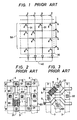
- Fig. 1 of the accompanying drawings shows the circuit structure of a major portion of a standard ROM, having a memory cell array 30, memory cells 31 consisting of MOS elements selectively formed using a mask pattern, data lines 40, and word lines 50.
- Figs. 2 and 3 of the accompanying drawings are plan views showing the structures of conventional ROM memory cells. Each of these figures shows a memory cell having four bits.
- the MOS transistors have gate electrodes 1 consisting of polycrystalline silicon which are connected together by aluminium lines of a first metal layer running in a horizontal direction in the figure, which lines constitute word lines 2. Diffusion layers are connected together by aluminium lines of a second metal layer running in a vertical direction, in the figure which lines constitute ground lines 3 and data lines 4.
- the words 'horizontal' and 'vertical' are used herein merely for ease of description; the device may be in any orientation.
- a thin oxide region either is or is not formed under the gate electrode 1 as reprsented by a hatched region 20 in Fig. 2. This is accomplished by changing the photomask of an isolation region 101 (usually by using local oxidation of silicon (LOCOS)).
- LOC local oxidation of silicon
- the word lines and data lines are usually formed by aluminium lines having a small wiring resistance. Therefore, the delay time of any interconnection line, given by the product of the parasitic capacitance and the parasitic resistance, is small, and operation can occur at high speeds.
- presence of as many as five contact holes 21 in the memory of four bits makes it difficult to reduce the area of the memory cells and, hence makes it difficult to increase the density of integration.
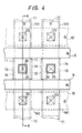
- gate electrodes of the transistors run in the horizontal direction in the figure to form word lines 5.
- ground lines 6 and data lines 7 are formed by aluminium lines of a first metal layer running in the vertical direction in the figure.
- a thin oxide film either is or is not formed on a region 8 indicated by hatched lines to write information into the memory cell.
- a thick insulator is formed (as for the isolation region) under the gate electrode (word line 5) in the right lower portion of Fig. 3, and information has already been written into the cell.
- Fig. 3 The structure of Fig. 3 has been disclosed in IEEE J. of SC "A 256 Kbit ROM with Serial ROM cell Structure", Roger Cuppens and L. H. M. Sevat, June, 1983, Vol. SC-18, No. 3.
- the number of contact holes 22 is as small as three for a memory of four bits, and the memory cell area can be reduced compared with that of the structure of Fig. 2.
- three aluminium layers one ground line and two data lines
- a limitation is imposed on further reduction of the area of the memory cell.
- the word lines are not straight and are long; i.e. the word lines have increased resistance and increased parasitic capacitance. Therefore, the structure of Fig. 3 is not advantageous for operating the ROM at high speed.
- US-A-4255210 shows an example of a read-only memory (ROM) discussed above which employs insulated gate field effect transistors comprising word lines extending linearly over a semiconductor substrate, ground lines, and data lines, the data lines intersecting, in plan view, the word lines. Furthermore, in US-A-4255210 a common source region is provided which extend substantially parallel to the word lines. That common source region is connected to a ground line and thus may be considered part of the ground line even though the terminology in US-A-4255210 is different.
- ROM read-only memory
- the present invention in a first aspect seeks to achieve a high density of integration and proposes that the ground lines comprise metal of the first metal layer, and the data lines comprise metal of the second metal layer.
- the linearity of the word lines minimises the parasitic capacitance and parasitic resistance, and the fact that the ground lines are parallel to the word lines permits a more compact geometrical arrangement.
- the ground lines comprise a first part and as second part, the first part being a semiconductor impurity region extending substantially parallel to the word lines, and the second part comprising metal of the first metal layer and extending substantially parallel to the data lines, and that the second metal layer is provided over the word lines through an insulator and electrically connected to the word line.
- the data lines preferably intersect the word lines approximately at right angles, and may be formed from the same metal layer as the ground lines, or the word and ground lines may be formed from the same metal layer.
- ground lines are located in the gaps between the word lines, but it is not necessary that they are provided in every such gap; in most arrangements it is preferable that they are provided in alternate gaps.
- the substrate, on which the word, ground, and data lines are formed, will normally have impurity regions in it, which impurity regions form the sources and drains of the insulated gate field effect transistors of the ROM.
- the drains are connected to the data lines either directly or via pads, and the ground lines are connected to the sources.
- the word lines then overlie the gates of the transistors.
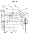
- Fig. 4 is a plan view of a memory of four bits according to a first embodiment of the present invention
- Fig. 5 is a section view along the line A-A' of Fig. 4.
- the data line 11 is formed by aluminium of a second metal layer.
- the pad 13 is not the one usually provided in LSI devices to make connection to the external unit, i.e., to effect wire bonding. Instead, the pad 13 connects the data line 11 to the n +- type diffusion layer 14 through the contact hole 25.
- the n +- type diffusion layer 14 acts as a common drain region for the two transistors that constitute adjacent memory cells, respectively. As shown in Fig. 5, furthermore, insulation films 15, 16 are interposed between the word lines, data lines and ground lines.
- the insulation films 15 may be composed of Si0 2 formed by thermally oxidizing a silicon substrate and/or polycrystalline silicon.
- the insulation films 15,16 may be composed of Si0 2 that is formed by the chemical vapor deposition CVD method or may be composed of other insulation films. It is convenient to form the insulation film 16 by the CVD method.
- the insulation films 15, 16 obtained by the above-mentioned methods are formed into desired shapes by a lithographic technique.
- Figs. 4 and 5 illustrate only two word lines 9
- additional word lines will normally be provided on the upper and lower sides of Fig. 4 to form MOS transistors that themselves form memory cells. Therefore, the n +- type diffusion layer 141 serves as a common source region for the MOS transistors.
- the structure shown in Fig. 4 repeats itself in the upper, lower, right and left directions to form a ROM which has a highly densely integrated form.
- the word lines 9 are not folded but run linearly in the horizontal direction, so that the length thereof is minimized. Therefore, the word lines have reduced parasitic resistance and reduced parasitic capacitance (and in particular the parasitic capacitance between the silicon substrate and the word lines is reduced), and the ROM may operate at high speeds.
- the delay time of the word lines may be reduced significantly, to enable a ROM that operates at very high speeds to be fabricated, if the word lines 9 are made of a metal having a small resistivity, such as tungsten (W), molybdenum (Mo), titanium (Ti), tantalum (Ta), or a silicide of these metals, or if the word lines 9 are composed of such metals or silicides thereof formed on the polycrystalline silicon. This is because, these materials have very small resis- tivites.
- the ground lines 10 are composed of metal lines of the first metal layer such as aluminium (Al) lines or tungsten (W) lines that run in the horizontal direction parallel to the word lines.
- the structure of such ground lines is altogether different from the structures shown in Figs. 2 and 3.
- the number of metal lines running in the vertical direction of the memory cell is two, which is smaller than the three metal lines of Fig. 3. Therefore, the lateral size of the ROM cell is greatly reduced, making it possible to fabricate the ROM cell in a highly integrated form.
- the individual patterns intersect substantially at right angles in the plane shown in Fig. 4, and the device can be designed so that its minimum size is determined by the processing technique. Therefore, the area of the ROM cell according to the present invention can be reduced, as compared with that of a ROM cell having a known structure prepared by the same process level, i.e.
- the ROM cell of the present invention it is also possible to reduce the area of the drain diffusion layer of each transistor compared with that of the structures shown in Figs. 2 and 3, and the junction capacitance of the diffusion layer, which produces about one-half the parasitic capacitance of the data line, also reduces, contributing to an increase in the speed of operation of the cell.
- the second aluminium layer which serves as the data line is connected to the diffusion layer 14 via the first aluminium layer.
- the insulation films 15, 16 under the data line 11 may have thicknesses greater than they could have when the data line is formed from the metal line of the first aluminium layer. Therefore, the distance between the data line and the substrate or the word line increases, and the parasitic capacitance of the data line decreases, also contributing to the increase in the operation speed of ROM cells.
- the data line 11 and the n +- type diffusion layer 141 may be connected together without necessarily providing the pad 13 by use of the first aluminium layer.
- the data line 11 (which is formed from a line of the second aluminium layer) may be directly connected to the n +- type diffusion layer 141 by forming a contact hole that penetrates through the insulation films 15 and 16.
- the parasitic capacitance of the data line may be decreased, as compared with conventional structures.
- the material for forming the ground lines 10, the data lines 11 and the pads 13 need not necessarily be aluminium.
- Other suitable material include e.g. tungsten (W), and molybdenum (Mo).
- Memory information can be written into the ROM cell of the present invention by forming an oxide film 231 under the word line 9 by using a mask pattern 17 in the hatched portion as shown in Fig. 6, i.e., by changing the threshold voltage of the MOS transistor.
- the information recorded depends on the thickness of the oxide film 231.
- memory information may be written into the cell by implanting impurities using a mask pattern 19 in the hatched portion.
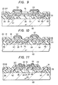
- Fig. 8 is a plan view of a memory of four bits according to a second embodiment of the present invention
- Figs. 9, 10 and 11 are sectional views along the line B-B', line C-C' and line E-E' thereof, respectively.
- electrically conductive lines 30 which consist of polycrystalline silicon, a silicide, or any other metal, and which form word lines
- electrically conductive lines 31 which consist of aluminium or any other metal and which form data lines
- electrically conductive lines 311 which are part of the same metal layer as the conductive lines 31 and which form a part of the ground lines.
- Intermediate layers 312 connect the word lines 30 to metal lines 33 which are located above the word lines 30 and are connected thereto via contact holes 36, 37.
- the ground lines also include diffusion layers 141 which diffusion layers 141 are connected to the metal ground lines 311 via contact holes 35.
- Other diffusion layers 14 serve as source or drain regions and are connected to data lines 31 via contact holes 34.
- a silicon dioxide layer forming an isolation region 39, and the substrate 60 of the device.
- the contact holes 34, 35, 36 under the metal lines of the first layer are formed separate from the contact holes 37 under the metal lines of the second layer on a plane.
- the two contact holes 24, 25 are superposed. Therefore, a large step exists in the portions of contact holes, and a difficulty exists in regard to forming the metal film.
- the layout of contact holes of the first embodiment gives advantage with regard to increasing the integration density.
- the word lines 30 are short-circuited by metal lines 33 made of aluminium, tungsten, or molybdenum having very small resistivity, giving an advantage if it is desired to operate the cell at high speeds.
- metal lines 33 made of aluminium, tungsten, or molybdenum having very small resistivity, giving an advantage if it is desired to operate the cell at high speeds.
- an additional area is required to connect the gate electrode 30 to the metal line 33 of the second layer, presenting a slight disadvantage from the standpoint of integration density as compared with the first embodiment.
- the data lines and the word lines are formed linearly, and intersect each other at right angles based upon the fundamental idea mentioned in the first embodiment.
- the second embodiment offers improvements with regard to high-speed operation and manufacturing process, but slightly sacrifices the integration density.
- memory information is written into the ROM cells in the same manner as the first embodiment.
- the thickness of the oxide film is reduced underthe word line 30 using a mask pattern in the hatched portion 38, and the threshold voltage of the MOS transistor is decreased to write memory information into the cell.
- the fundamental idea of the present invention can also be maintained even if the metal lines of the first layer and the metal lines of the second layer are used in a reversed manner in the second embodiment.
- the resistance of the diffusion layers 141 which form part of the ground lines may be further reduced by forming silicides of W, Mo, Ti, Ta etc. or refractory metals such as W, Mo etc. on the diffusion layers.
- the present invention makes if possible to achieve highly integrated memory cells for a ROM, which cells require an area which is reduced to one-half to one-fifth that of the conventional structures. Furthermore, according to the present invention, parasitic resistance and parasitic capacitance of the word lines and data lines may be decreased, enabling the ROM to operate at high speeds.
- the memory cells for ROM of the present invention may be made up of either n-channel MOS transistors or p-channel MOS transistors using a silicon semiconductor.
- Compound semi-conductors can also be used such as SOS (silicon on sapphire), SOI (silicon on insulation), GaAs, and the like.
- SOS silicon on sapphire
- SOI silicon on insulation
- GaAs GaAs
Landscapes
- Semiconductor Memories (AREA)
- Read Only Memory (AREA)
Claims (12)
Applications Claiming Priority (2)
| Application Number | Priority Date | Filing Date | Title |
|---|---|---|---|
| JP137537/83 | 1983-07-29 | ||
| JP58137537A JPS6030170A (ja) | 1983-07-29 | 1983-07-29 | 高集積読み出し専用メモリ |
Publications (3)
| Publication Number | Publication Date |
|---|---|
| EP0133023A2 EP0133023A2 (de) | 1985-02-13 |
| EP0133023A3 EP0133023A3 (en) | 1986-07-02 |
| EP0133023B1 true EP0133023B1 (de) | 1990-06-13 |
Family
ID=15201000
Family Applications (1)
| Application Number | Title | Priority Date | Filing Date |
|---|---|---|---|
| EP84305083A Expired EP0133023B1 (de) | 1983-07-29 | 1984-07-26 | Nur-Lesespeicher |
Country Status (5)
| Country | Link |
|---|---|
| US (1) | US4707718A (de) |
| EP (1) | EP0133023B1 (de) |
| JP (1) | JPS6030170A (de) |
| KR (1) | KR920010196B1 (de) |
| DE (1) | DE3482529D1 (de) |
Families Citing this family (15)
| Publication number | Priority date | Publication date | Assignee | Title |
|---|---|---|---|---|
| KR880700464A (ko) * | 1985-07-29 | 1988-03-15 | 마이클 와이.엡스타인 | 집적 회로에 대한 세 레벨 상호 연결 기법 |
| JP2511485B2 (ja) * | 1988-01-12 | 1996-06-26 | 沖電気工業株式会社 | 半導体記憶装置 |
| JP2765583B2 (ja) * | 1988-10-20 | 1998-06-18 | 株式会社リコー | 半導体メモリ装置 |
| US5301349A (en) * | 1988-12-28 | 1994-04-05 | Kabushiki Kaisha Toshiba | Single chip computer having ground wire formed immediately parallel a data bus and drivers formed directly under the data bus for high speed data transfer |
| JP2901188B2 (ja) * | 1988-12-28 | 1999-06-07 | 株式会社東芝 | 半導体集積回路 |
| KR930003273B1 (ko) * | 1989-03-14 | 1993-04-24 | 가부시키가이샤 도시바 | 반도체장치 |
| JPH07114258B2 (ja) * | 1989-09-13 | 1995-12-06 | 東芝マイクロエレクトロニクス株式会社 | 半導体メモリ |
| US5117389A (en) * | 1990-09-05 | 1992-05-26 | Macronix International Co., Ltd. | Flat-cell read-only-memory integrated circuit |
| EP0558133B1 (de) * | 1992-02-27 | 1997-06-18 | Koninklijke Philips Electronics N.V. | Integrierte CMOS-Schaltung |
| US5291435A (en) * | 1993-01-07 | 1994-03-01 | Yu Shih Chiang | Read-only memory cell |
| US5380676A (en) * | 1994-05-23 | 1995-01-10 | United Microelectronics Corporation | Method of manufacturing a high density ROM |
| TW583431B (en) * | 2000-02-22 | 2004-04-11 | Toshiba Corp | Liquid crystal display device |
| US6646312B1 (en) * | 2000-07-28 | 2003-11-11 | Oki Electric Industry Co., Ltd. | Semiconductor memory device with bit lines having reduced cross-talk |
| JP2003224212A (ja) * | 2002-01-30 | 2003-08-08 | Mitsubishi Electric Corp | 半導体装置及びその製造方法 |
| EP4002453B1 (de) * | 2020-05-28 | 2025-03-26 | Changxin Memory Technologies, Inc. | Ausleitstruktur für wortleitung und verfahren zu ihrer herstellung |
Family Cites Families (10)
| Publication number | Priority date | Publication date | Assignee | Title |
|---|---|---|---|---|
| JPS51111020A (en) * | 1975-03-26 | 1976-10-01 | Hitachi Ltd | Semiconductor fixing memory equipment |
| JPS54121685A (en) * | 1978-03-14 | 1979-09-20 | Kyushu Nippon Electric | Ic and method of fabricating same |
| JPS5571063A (en) * | 1978-11-24 | 1980-05-28 | Hitachi Ltd | Semiconductor fixed memory |
| EP0014388B1 (de) * | 1979-01-25 | 1983-12-21 | Nec Corporation | Halbleiterspeicher-Vorrichtung |
| US4282646A (en) * | 1979-08-20 | 1981-08-11 | International Business Machines Corporation | Method of making a transistor array |
| JPS56157056A (en) * | 1980-05-09 | 1981-12-04 | Fujitsu Ltd | Manufacture of read-only memory |
| EP0054102A3 (de) * | 1980-12-11 | 1983-07-27 | Rockwell International Corporation | ROM-Zellen in sehr dichter Anordnung und Herstellungsverfahren |
| US4380866A (en) * | 1981-05-04 | 1983-04-26 | Motorola, Inc. | Method of programming ROM by offset masking of selected gates |
| US4358889A (en) * | 1981-05-28 | 1982-11-16 | General Motors Corporation | Process for making a late programming enhanced contact ROM |
| DE3380548D1 (en) * | 1982-03-03 | 1989-10-12 | Fujitsu Ltd | A semiconductor memory device |
-
1983
- 1983-07-29 JP JP58137537A patent/JPS6030170A/ja active Pending
-
1984
- 1984-07-23 KR KR1019840004348A patent/KR920010196B1/ko not_active Expired
- 1984-07-26 EP EP84305083A patent/EP0133023B1/de not_active Expired
- 1984-07-26 DE DE8484305083T patent/DE3482529D1/de not_active Expired - Lifetime
- 1984-07-30 US US06/635,401 patent/US4707718A/en not_active Expired - Fee Related
Also Published As
| Publication number | Publication date |
|---|---|
| US4707718A (en) | 1987-11-17 |
| KR920010196B1 (ko) | 1992-11-19 |
| EP0133023A2 (de) | 1985-02-13 |
| EP0133023A3 (en) | 1986-07-02 |
| JPS6030170A (ja) | 1985-02-15 |
| DE3482529D1 (de) | 1990-07-19 |
| KR850000799A (ko) | 1985-03-09 |
Similar Documents
| Publication | Publication Date | Title |
|---|---|---|
| EP0133023B1 (de) | Nur-Lesespeicher | |
| JP2989579B2 (ja) | Dramセル構造、およびnvramセル構造を単一の基板に形成する方法およびこれら構造を単一の基板に含む半導体メモリ・デバイス | |
| US4970564A (en) | Semiconductor memory device having stacked capacitor cells | |
| KR100724029B1 (ko) | 반도체 장치 및 트랜지스터 | |
| US4992389A (en) | Making a self aligned semiconductor device | |
| KR0120926B1 (ko) | 반도체 집적회로 장치 및 그 제조방법 | |
| US5818090A (en) | Semiconductor devices with load elements | |
| US5012443A (en) | Semiconductor static ram including load resistors formed on different layers | |
| JP4471504B2 (ja) | 半導体記憶装置 | |
| WO1992002042A1 (en) | Compact sram cell layout | |
| US4807017A (en) | Semiconductor memory device with wirings having ensured cross-sections | |
| JP3896214B2 (ja) | 半導体メモリデバイス及びその製造方法 | |
| JPH0328831B2 (de) | ||
| US5610856A (en) | Semiconductor integrated circuit device | |
| JP3940495B2 (ja) | Sramセルの構造及びその製造方法 | |
| JP3539705B2 (ja) | 半導体記憶装置 | |
| US6455899B2 (en) | Semiconductor memory device having improved pattern of layers and compact dimensions | |
| US6407463B2 (en) | Semiconductor memory device having gate electrode, drain-drain contact, and drain-gate contact layers | |
| JP2000040388A (ja) | 半導体メモリ装置とその作製方法 | |
| US6653696B2 (en) | Semiconductor device, memory system, and electronic instrument | |
| US5227319A (en) | Method of manufacturing a semiconductor device | |
| JP2689940B2 (ja) | スタティック型メモリセル | |
| JP2770348B2 (ja) | 半導体記憶装置 | |
| JPS60167360A (ja) | 半導体記憶装置 | |
| JPH02106966A (ja) | 半導体記憶装置 |
Legal Events
| Date | Code | Title | Description |
|---|---|---|---|
| PUAI | Public reference made under article 153(3) epc to a published international application that has entered the european phase |
Free format text: ORIGINAL CODE: 0009012 |
|
| 17P | Request for examination filed |
Effective date: 19840831 |
|
| AK | Designated contracting states |
Designated state(s): DE FR GB IT |
|
| PUAL | Search report despatched |
Free format text: ORIGINAL CODE: 0009013 |
|
| AK | Designated contracting states |
Kind code of ref document: A3 Designated state(s): DE FR GB IT |
|
| 17Q | First examination report despatched |
Effective date: 19880329 |
|
| GRAA | (expected) grant |
Free format text: ORIGINAL CODE: 0009210 |
|
| AK | Designated contracting states |
Kind code of ref document: B1 Designated state(s): DE FR GB IT |
|
| REF | Corresponds to: |
Ref document number: 3482529 Country of ref document: DE Date of ref document: 19900719 |
|
| ET | Fr: translation filed | ||
| ITF | It: translation for a ep patent filed | ||
| PLBE | No opposition filed within time limit |
Free format text: ORIGINAL CODE: 0009261 |
|
| STAA | Information on the status of an ep patent application or granted ep patent |
Free format text: STATUS: NO OPPOSITION FILED WITHIN TIME LIMIT |
|
| 26N | No opposition filed | ||
| ITTA | It: last paid annual fee | ||
| PGFP | Annual fee paid to national office [announced via postgrant information from national office to epo] |
Ref country code: DE Payment date: 19970925 Year of fee payment: 14 |
|
| PGFP | Annual fee paid to national office [announced via postgrant information from national office to epo] |
Ref country code: GB Payment date: 19980624 Year of fee payment: 15 |
|
| PGFP | Annual fee paid to national office [announced via postgrant information from national office to epo] |
Ref country code: FR Payment date: 19980710 Year of fee payment: 15 |
|
| PG25 | Lapsed in a contracting state [announced via postgrant information from national office to epo] |
Ref country code: DE Free format text: LAPSE BECAUSE OF NON-PAYMENT OF DUE FEES Effective date: 19990501 |
|
| PG25 | Lapsed in a contracting state [announced via postgrant information from national office to epo] |
Ref country code: GB Free format text: LAPSE BECAUSE OF NON-PAYMENT OF DUE FEES Effective date: 19990726 |
|
| PG25 | Lapsed in a contracting state [announced via postgrant information from national office to epo] |
Ref country code: FR Free format text: THE PATENT HAS BEEN ANNULLED BY A DECISION OF A NATIONAL AUTHORITY Effective date: 19990731 |
|
| GBPC | Gb: european patent ceased through non-payment of renewal fee |
Effective date: 19990726 |
|
| REG | Reference to a national code |
Ref country code: FR Ref legal event code: ST |