EP0135039A1 - Réduction du bruit par interpolation linéaire au moyen d'un circuit d'échantillonnage et de maintien simple - Google Patents
Réduction du bruit par interpolation linéaire au moyen d'un circuit d'échantillonnage et de maintien simple Download PDFInfo
- Publication number
- EP0135039A1 EP0135039A1 EP84108562A EP84108562A EP0135039A1 EP 0135039 A1 EP0135039 A1 EP 0135039A1 EP 84108562 A EP84108562 A EP 84108562A EP 84108562 A EP84108562 A EP 84108562A EP 0135039 A1 EP0135039 A1 EP 0135039A1
- Authority
- EP
- European Patent Office
- Prior art keywords
- voltage
- capacitor
- output
- differentiator
- amplifier
- Prior art date
- Legal status (The legal status is an assumption and is not a legal conclusion. Google has not performed a legal analysis and makes no representation as to the accuracy of the status listed.)
- Granted
Links
- 230000009467 reduction Effects 0.000 title claims abstract description 16
- 239000003990 capacitor Substances 0.000 claims abstract description 48
- 238000005070 sampling Methods 0.000 claims description 18
- 230000000694 effects Effects 0.000 claims description 4
- 230000003321 amplification Effects 0.000 claims description 3
- 238000003199 nucleic acid amplification method Methods 0.000 claims description 3
- 230000004044 response Effects 0.000 abstract description 5
- 230000005236 sound signal Effects 0.000 description 10
- 230000009471 action Effects 0.000 description 5
- 230000003111 delayed effect Effects 0.000 description 5
- 238000010586 diagram Methods 0.000 description 4
- 238000001228 spectrum Methods 0.000 description 3
- 238000000034 method Methods 0.000 description 2
- 230000008859 change Effects 0.000 description 1
- 230000004069 differentiation Effects 0.000 description 1
- 230000036039 immunity Effects 0.000 description 1
- 230000008569 process Effects 0.000 description 1
- 230000001960 triggered effect Effects 0.000 description 1
Images




Classifications
-
- H—ELECTRICITY
- H03—ELECTRONIC CIRCUITRY
- H03K—PULSE TECHNIQUE
- H03K17/00—Electronic switching or gating, i.e. not by contact-making and –breaking
-
- H—ELECTRICITY
- H03—ELECTRONIC CIRCUITRY
- H03G—CONTROL OF AMPLIFICATION
- H03G3/00—Gain control in amplifiers or frequency changers
- H03G3/20—Automatic control
- H03G3/30—Automatic control in amplifiers having semiconductor devices
- H03G3/34—Muting amplifier when no signal is present
- H03G3/345—Muting during a short period of time when noise pulses are detected, i.e. blanking
Definitions
- the present invention relates to a noise reduction circuit of the type wherein noise-affected portion of an information signal is linearly interpolated.
- Linear interpolation techniques are known in the art as a means for reconstructing the portion of audio signals which is disrupted by a noise impulse, as shown and described in the above listed copending U.S. applications.
- the linear interpolation approach employed in the aforesaid applications involves the use of two sample-and-hold circuits; one connected in a circuit between input and output terminals for generating a voltage which follows the waveform of the input signal during tracking modes and storing a voltage immediately prior to the occurrence of a noise impulse and subsequently performing charge or dishcharge action during a sampling mode and the other for generating an interpolation voltage representing the rate of variation of the information signal to allow the first one to perform the charge or discharge action in accordance with the interpolation voltage.
- An object of the present invention is eliminate the need for the second sample-and-hold circuit to provide a simplified noise reduction circuit.
- the noise reduction circuit of the present invention comprises a noise detector connected to an input terminal to which an information signal is applied for detecting a noise impulse introduced therein and generating a sampling pulse time-coincident with the portion of the signal affected by the impulse.
- a sample-and-hold circuit connected between the input and output terminals, includes a capacitor and a switch for passing the information signal to the output terminal in the absence of the sampling signal.
- a slope detector is responsive to a voltage developed in the capacitor for generating a voltage representative of the rate of variation of the capacitor voltage. Further provided is a voltage-to-current converter connected between the output of the slope detector and the capacitor for converting the voltage to a corresponding current and injecting the current to the capacitor when the rate of variation is positive and draining the current from the capacitor when the rate is negative.
- the slope detector comprises a first differentiator connected to the sample-and-hold circuit and a second differentiator connected to the first differentiator.
- the outputs of the first and second differentiators are combined and applied to the voltage-to-current converter.
- the first differentiator has a time constant value greater than 1/(2 ⁇ fm), where fm represents the highest frequency of the information signal so that the output of the first differentiator becomes substantially constant when the information signal has a frequency lower than 1/(2 ⁇ T 1 ) where T 1 is the time constant value.
- the slope detector further includes an amplifier for amplifying the combined differentiator output.
- the amplification gain of this amplifier is such that when the frequency of the information signal is lower than 1/(2 ⁇ T 1 ) a voltage at the output of the amplifier substantially equals the voltage developed in the capacitor.
- the voltage-to-current converter can advantageously be constituted by an impedance element, or resistor.
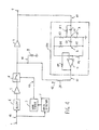
- the signal applied to an input terminal 1 is an audio signal which may be derived from an audio track of a videotape, the input signal being applied to a noise detector 2.
- a noise impulse as shown at 20 in Fig. 2, by which the signal is disrupted, is detected and a pulse of a duration T equal to the disrupted portion is produced by noise detector 2 and applied to a waveshaper 3 for generating a sampling pulse having sharp edges as shown at 21 in Fig. 2.
- the audio signal is also applied through a delay circuit 4, an amplifier 5 having a low output impedance, an electronic switch 6 and through.a second amplifier 7 having a high input impedance to an output terminal 9 to which noise-suppressed signal is delivered.
- Switch 6 is of a normally closed contact type which cuts off the circuit between input and output terminals 1 and 9 in response to a sampling pulse provided by waveshaper 3.
- the audio signal is delayed in the circuit 4 so that its noise-affected portion is time coincident with the sampling pulse.
- capacitor 8 To a node between switch 6 and amplifier 7 is connected a "holding" capacitor 8 which is grounded. Since the switch 6 is normally closed in the absense of noise impulses, capacitor 8 is normally charged to a voltage level that varies with the waveform of the input signal and "freezes" the voltage which appeared immediately prior to the switch being opened in response to sampling pulse.
- a slope detector 10 To the output of amplifier 7 is connected a slope detector 10.
- This detector comprises a first differentiator formed by capacitor Cl and resistor Rl, and a second differentiator formed by capacitor C2 and resistor R2.
- the first differentiator differentiates the output of amplifier 7 so that its output is 90 0 out of phase with the input signal.
- the second differentiator is connected to the node between capacitor Cl and resistor Rl to provide double differentiation of the audio output.
- a first differentiator output appears at a node between capacitor Cl and resistor Rl and a second differentiator output appears at a node between capacitor C2 and resistor R2, the voltages appearing at these nodes being combined by resistors R3 and R4 in such a proportion that, as will be described, a voltage developed in capaictor 8 during hold mode adequately interpolates the disrupted portion of the audio signal.
- the combined differentiators output is applied to the positive input of an operational amplifier 11 which constitutes an noninverting amplifier with a feedback resistor R5 and a bias resistor R6 the junction of which is coupled to the negative input of amplifier 11.
- the output of amplifier 11 represents an estimated value of the slope between the noise-disrupted portion of the audio signal, this output being delayed by a delay circuit 12 and fed to the input of a voltage-to-current converter, or bipolar constant current source 13 whose output is connected to capacitor 8.
- Delay circuit 12 can be dispensed with if the sampling pulse lasts as long as 30 microseconds since the feedback loop has an inherent delay time of the order of microseonds.
- the operation of the noise reduction circuit is as follows. In the absence of impulsive noise, the output of the constant current source 13 sees a low impedance path through the output of amplifier 5 via switch 6 which is in a closed state. Thus, the voltage on capacitor 8 is not influenced under the effect of the constant current source during such modes and capacitor 8 allows the voltage to follow the waveform of the input audio signal.
- Slope detector 10 generates an output shown at 22 in Fig. 2 which is out of phase with the input waveform 23 and is delayed by an amount t in delay circuit 12 providing a delayed output 24 which drives the constant current source 13.
- This constant current source includes a pair of transistors 19 and 20 of opposite conductivity types connected in series through resistors 17 and 18 to positive and negative voltage sources, with the junction between them being coupled to capacitor 8.
- a biasing resistor network comprising a series combination of resistors 14, 15 and 16 biases transistors 19 and 20 with positive and negative voltages, respectively.
- sampling pulse 2 is applied to switch 6 time coincident with the noise impulse to cut off the channel between input and output terminals 1 and 9.
- the voltage developed in capacitor 8 at the moment immediately prior to the leading edge of sampling pulse is sampled and frozen in that capacitor. Since this voltage represents the location of the noise impulse in the excursion of the waveform, the input signal fed through amplifier 7 to slope detector 10 indicates whether the disrupted portion is to be interpolated with a positive or negative slope. In the illustrated example, the noise impulse is assumed to have occurred on a negative slope of the audio signal. Immediately prior to the occurrence of sampling pulse 21, slope detector 10 is generating a negative voltage.
- slope detector 10 continues its differentiating action, so that it generates a negative voltage. Due to the delay time t ot the loop, the current to be injected to capacitor 8 is derived from a voltage which occurred in capacitor 8 t period earlier than the time the sampling pulse occurred.
- the negative voltage drives transistor 20 into conduction and drains a current from capacitor 8 by an amount proportional to the negative voltage.
- the voltage at the output of amplifier 7, shown at 25 in Fig. 2 begins to decrease linearly as indicated by a thick line 26.
- the loop's delayed action enables the slope detector to respond to a successive change in voltage output from amplifier 7 by generating a voltage of a constant value as indicated by a thick line 27. This process is repeated until the end of the period T. As a result, the current drained from capacitor 8 will appear as indicated at 28, and the noise-affected portion of the waveform 25 is linearly interpolated by slope voltage 26.
- slope detector 10 will generate a positive interpolation voltage which turns on sransistor 19 to inject a current into capacitor 8.
- the loop gain of the closed loop interpolation is appropriately determined by the ratio (R5 + R6)/R6, for example. If the loop gain is too low, the voltage section 26 would follow an upper path indicated by a broken-line 26a in Fig. 3 and if too high, the voltage would follow a lower path indicated by a broken line 26b.
- the constant current source is formed by a single impedance element or resistor 30 and slope detector 10a differs from that shown in Fig. 1 by the inclusion of a resistor R7 connected in parallel with capacitor Cl.
- resistor R7 and capacitor Cl are dominant factors in determining the time constant value of the first differentiator and for higher frequency signals, resistor R1 becomes dominant in addition to R7 and Cl so that first differentiator has two time constant values T 1 and T 2 for lower and higher frequency signals, respectively, as given below:
- T 2 is given by:
- time constant T 2 is much smaller than the period 1/(2 ⁇ fm), where fm represents the highest frequency of the audio spectrum.
- the phase-vs-trequcncy characteristic indicates a peak at a point close to the highest frequency value fm and the phase gradually increases with frequency from zero degree within the audio frequency spectrum W.
- the level-vs-frequency and phase-vs-frequency characteristics of the second differentiator measured at node B show similar tendencies to those of Fig. 5a as indicated at 32L and 32P in Fig. 5b, respectively.
- resistance values of R3 and R4 are sufficiently high in comparison with the resistances Rl, R2 and R4 to minimize their effects on the time constant values of the two differentiators.
- the loop gain of the system which is determined exclusively by the ratio (R5 + R6)/R6, is determined so that the output level of amplifier 11 is substantially equal to the voltage developed in capacitor 8 when the frequency of the audio signal is lower than f 1 .
- the resultant level-vs-frequency characteristic of slope detector 10a shows a tendency to approach the 0-dB level with a decrease in frequency.
- the phase-vs-frequency characteristic, shown at 33P has a near-90° peak value at a point slightly lower than fm.
- the level-vs-frequency and phase-vs-frequency characterstics measured at capacitor 8 are flat over the frequency spectrum W and beyond as indicated at 34L and 34P, respectively, in Fig. 5d.
- the voltage waveform shown at 40 in Fig. 6 is a signal delivered to output terminal 9 and the difference between it and an output voltage 41 of slope detector lOa is thus taken and this difference, shown at 42, is proportional to the gradient of the voltage 40 and flows through resistor 30. It is seen in Fig. 6 that current 42 is advanced in phase with respect to the output 41 of slope detector 10a, In response to a noise-triggered sampling pulse 43, current 44 begins to flow into or out of capacitor 8 depending on the location of the noise impulse 45 on the waveform of input signal 46.
- the interpolation loop has an inherent loop delay on the order of microseconds as described in the previous embodiment and this loop delay is not explicitly shown in Fig. 4. Due to this inherent loop delay, the voltage developed by slope detector 10a at the moment switch 6 is opened represents the slope of the audio input signal immediately prior to the occurrence of the switching action. By using this starting voltage, linear interpolation proceeds until the switch is closed.
- Amplifier 7 has a 0-dB amplification gain.
- the voltage delivered to output terminal 9 is therefore substantially equal to that developed in capacitor 8.
- the voltage-to-current converter or constant-current source is greatly simplified and there is no need to use a second sample-and-hold circuit which is employed in the aforesaid copending applications.
Landscapes
- Noise Elimination (AREA)
- Amplifiers (AREA)
Applications Claiming Priority (4)
| Application Number | Priority Date | Filing Date | Title |
|---|---|---|---|
| JP13312883A JPS6024716A (ja) | 1983-07-21 | 1983-07-21 | 信号補間回路 |
| JP133128/83 | 1983-07-21 | ||
| JP15566883A JPS6046621A (ja) | 1983-08-25 | 1983-08-25 | 信号補間回路 |
| JP155668/83 | 1983-08-25 |
Publications (2)
| Publication Number | Publication Date |
|---|---|
| EP0135039A1 true EP0135039A1 (fr) | 1985-03-27 |
| EP0135039B1 EP0135039B1 (fr) | 1988-09-28 |
Family
ID=26467550
Family Applications (1)
| Application Number | Title | Priority Date | Filing Date |
|---|---|---|---|
| EP84108562A Expired EP0135039B1 (fr) | 1983-07-21 | 1984-07-19 | Réduction du bruit par interpolation linéaire au moyen d'un circuit d'échantillonnage et de maintien simple |
Country Status (4)
| Country | Link |
|---|---|
| US (1) | US4555669A (fr) |
| EP (1) | EP0135039B1 (fr) |
| KR (1) | KR900004194B1 (fr) |
| DE (1) | DE3474390D1 (fr) |
Cited By (2)
| Publication number | Priority date | Publication date | Assignee | Title |
|---|---|---|---|---|
| EP1860781A4 (fr) * | 2005-03-17 | 2010-06-09 | Pioneer Corp | Systeme de suppression du bruit |
| EP1860780A4 (fr) * | 2005-03-16 | 2010-06-09 | Pioneer Corp | Dispositif d'annulation de bruit |
Families Citing this family (10)
| Publication number | Priority date | Publication date | Assignee | Title |
|---|---|---|---|---|
| JPS61184933A (ja) * | 1985-02-12 | 1986-08-18 | Clarion Co Ltd | パルス性雑音除去用信号補償ゲ−ト回路 |
| JPS62132434A (ja) * | 1985-12-05 | 1987-06-15 | Clarion Co Ltd | ゲ−ト回路 |
| US4924115A (en) * | 1989-02-21 | 1990-05-08 | Xerox Corporation | Integrated circuit RC filters with very large time constants |
| KR0182943B1 (ko) * | 1995-02-04 | 1999-04-15 | 김광호 | 오디오신호의 잡음 제거 회로 |
| US5859392A (en) * | 1996-02-09 | 1999-01-12 | Lsi Logic Corporation | Method and apparatus for reducing noise in an electrostatic digitizing tablet |
| IT1308062B1 (it) * | 1999-05-28 | 2001-11-29 | St Microelectronics Srl | Circuito di protezione per ridurre il rumore sui riferimenti ditensione, in particolare in convertitori dc-dc |
| US6359504B1 (en) * | 2000-01-28 | 2002-03-19 | Lucent Technologies Inc. | Power amplifier using upstream signal information |
| DE60143193D1 (de) * | 2000-02-07 | 2010-11-18 | Draeger Medical Systems Inc | Abtastvorrichtung mit optimierter abtastrate |
| US7724042B2 (en) * | 2007-07-06 | 2010-05-25 | Texas Instruments Incorporated | Reducing power consumption in an amplification stage driving a sample and hold circuit while maintaining linearity |
| WO2012027327A2 (fr) * | 2010-08-24 | 2012-03-01 | Cypress Semiconductor Corporation | Circuits de suppression de bruit et procédés en rapport avec des systèmes de détection de capacitance |
Citations (3)
| Publication number | Priority date | Publication date | Assignee | Title |
|---|---|---|---|---|
| DE2262560A1 (de) * | 1972-12-21 | 1974-06-27 | Blaupunkt Werke Gmbh | Verfahren und vorrichtung zum unterdruecken von stoerungen in einem elektrischen signal |
| DE2929030A1 (de) * | 1978-07-18 | 1980-02-07 | Matsushita Electric Ind Co Ltd | Verfahren zur stoerimpulsunterdrueckung |
| EP0103385A2 (fr) * | 1982-07-30 | 1984-03-21 | Victor Company Of Japan, Limited | Montage pour reconstituer des signaux affectés par du bruit parasite |
Family Cites Families (3)
| Publication number | Priority date | Publication date | Assignee | Title |
|---|---|---|---|---|
| JPS5514734A (en) * | 1978-07-17 | 1980-02-01 | Nec Corp | Pulse noise elimination circuit |
| US4335322A (en) * | 1979-09-17 | 1982-06-15 | Nippon Electric Co., Ltd. | Pulse generator for producing a pulse having a pulse width dependent on an input signal |
| JPS5795728A (en) * | 1980-12-05 | 1982-06-14 | Nippon Gakki Seizo Kk | Impulse noise eliminating device |
-
1984
- 1984-07-19 EP EP84108562A patent/EP0135039B1/fr not_active Expired
- 1984-07-19 DE DE8484108562T patent/DE3474390D1/de not_active Expired
- 1984-07-20 US US06/632,875 patent/US4555669A/en not_active Expired - Lifetime
- 1984-07-21 KR KR1019840004333A patent/KR900004194B1/ko not_active Expired
Patent Citations (3)
| Publication number | Priority date | Publication date | Assignee | Title |
|---|---|---|---|---|
| DE2262560A1 (de) * | 1972-12-21 | 1974-06-27 | Blaupunkt Werke Gmbh | Verfahren und vorrichtung zum unterdruecken von stoerungen in einem elektrischen signal |
| DE2929030A1 (de) * | 1978-07-18 | 1980-02-07 | Matsushita Electric Ind Co Ltd | Verfahren zur stoerimpulsunterdrueckung |
| EP0103385A2 (fr) * | 1982-07-30 | 1984-03-21 | Victor Company Of Japan, Limited | Montage pour reconstituer des signaux affectés par du bruit parasite |
Non-Patent Citations (1)
| Title |
|---|
| PATENT ABSTRACTS OF JAPAN, vol. 6, no. 182, 18 September 1982 & JP-A-57-095728 (NIPPON GAKKI SEIZO K.K.) 14-06-1982 * |
Cited By (2)
| Publication number | Priority date | Publication date | Assignee | Title |
|---|---|---|---|---|
| EP1860780A4 (fr) * | 2005-03-16 | 2010-06-09 | Pioneer Corp | Dispositif d'annulation de bruit |
| EP1860781A4 (fr) * | 2005-03-17 | 2010-06-09 | Pioneer Corp | Systeme de suppression du bruit |
Also Published As
| Publication number | Publication date |
|---|---|
| US4555669A (en) | 1985-11-26 |
| EP0135039B1 (fr) | 1988-09-28 |
| KR850001644A (ko) | 1985-03-30 |
| DE3474390D1 (en) | 1988-11-03 |
| KR900004194B1 (ko) | 1990-06-18 |
Similar Documents
| Publication | Publication Date | Title |
|---|---|---|
| US4463320A (en) | Automatic gain control circuit | |
| US4555669A (en) | Noise reduction by linear interpolation using a single sample-and-hold circuit | |
| US3678416A (en) | Dynamic noise filter having means for varying cutoff point | |
| US4112384A (en) | Controlled recovery automatic gain control amplifier | |
| US4433256A (en) | Limiter with dynamic hysteresis | |
| US6556685B1 (en) | Companding noise reduction system with simultaneous encode and decode | |
| US3947636A (en) | Transient noise filter employing crosscorrelation to detect noise and autocorrelation to replace the noisey segment | |
| EP0135081B1 (fr) | Réduction de bruit par interpolation linéaire utilisant un circuit amplificateur à double fonction | |
| EP0066110A2 (fr) | Dispositif d'élimination de bruit dans un récepteur FM | |
| US4207527A (en) | Pre-processing apparatus for FM stereo overshoot elimination | |
| EP0103385B1 (fr) | Montage pour reconstituer des signaux affectés par du bruit parasite | |
| US4577161A (en) | Noise reduction by linear interpolation using a dual function amplifier circuit | |
| US3769592A (en) | Squench circuit with time delay variable in accordance with strength of received signal | |
| EP0099760B1 (fr) | Circuit pour reconstituer des signaux affectés par du bruit parasite | |
| US3278866A (en) | Selective transmission | |
| US4531095A (en) | Impulse noise reduction by linear interpolation having immunity to white noise | |
| US4370620A (en) | Efficient high performance envelope detector with controlled decay envelope detection | |
| US4490838A (en) | Muting circuit for AM stereophonic receiver | |
| US4106063A (en) | Circuit arrangement for a dropout detector | |
| US3873925A (en) | Audio frequency squelch system | |
| US4140928A (en) | Monostable multivibrator | |
| US4532475A (en) | Impulse noise reduction by linear interpolation having a deemphasis characteristic | |
| GB1563873A (en) | Noise clearing system | |
| US3319013A (en) | Apparatus for recording high frequency signals on magnetic tape | |
| US4208634A (en) | Circuit for suppressing noise caused by scratches on a phonograph record |
Legal Events
| Date | Code | Title | Description |
|---|---|---|---|
| PUAI | Public reference made under article 153(3) epc to a published international application that has entered the european phase |
Free format text: ORIGINAL CODE: 0009012 |
|
| AK | Designated contracting states |
Designated state(s): DE FR NL |
|
| 17P | Request for examination filed |
Effective date: 19850327 |
|
| 17Q | First examination report despatched |
Effective date: 19861027 |
|
| GRAA | (expected) grant |
Free format text: ORIGINAL CODE: 0009210 |
|
| AK | Designated contracting states |
Kind code of ref document: B1 Designated state(s): DE FR NL |
|
| REF | Corresponds to: |
Ref document number: 3474390 Country of ref document: DE Date of ref document: 19881103 |
|
| ET | Fr: translation filed | ||
| PLBE | No opposition filed within time limit |
Free format text: ORIGINAL CODE: 0009261 |
|
| STAA | Information on the status of an ep patent application or granted ep patent |
Free format text: STATUS: NO OPPOSITION FILED WITHIN TIME LIMIT |
|
| 26N | No opposition filed | ||
| PGFP | Annual fee paid to national office [announced via postgrant information from national office to epo] |
Ref country code: FR Payment date: 20030711 Year of fee payment: 20 |
|
| PGFP | Annual fee paid to national office [announced via postgrant information from national office to epo] |
Ref country code: NL Payment date: 20030730 Year of fee payment: 20 |
|
| PGFP | Annual fee paid to national office [announced via postgrant information from national office to epo] |
Ref country code: DE Payment date: 20030731 Year of fee payment: 20 |
|
| PG25 | Lapsed in a contracting state [announced via postgrant information from national office to epo] |
Ref country code: NL Free format text: LAPSE BECAUSE OF EXPIRATION OF PROTECTION Effective date: 20040719 |
|
| NLV7 | Nl: ceased due to reaching the maximum lifetime of a patent |
Effective date: 20040719 |