EP0135407B1 - Anordnung zur Verteilung und Zusammenführung von Mikrowellenenergie und damit aufgebauter Mikrowellenleistungsverstärker - Google Patents
Anordnung zur Verteilung und Zusammenführung von Mikrowellenenergie und damit aufgebauter Mikrowellenleistungsverstärker Download PDFInfo
- Publication number
- EP0135407B1 EP0135407B1 EP84401431A EP84401431A EP0135407B1 EP 0135407 B1 EP0135407 B1 EP 0135407B1 EP 84401431 A EP84401431 A EP 84401431A EP 84401431 A EP84401431 A EP 84401431A EP 0135407 B1 EP0135407 B1 EP 0135407B1
- Authority
- EP
- European Patent Office
- Prior art keywords
- distributing
- electric field
- synthesizing
- base
- microwave
- Prior art date
- Legal status (The legal status is an assumption and is not a legal conclusion. Google has not performed a legal analysis and makes no representation as to the accuracy of the status listed.)
- Expired
Links
Images




Classifications
-
- H—ELECTRICITY
- H03—ELECTRONIC CIRCUITRY
- H03F—AMPLIFIERS
- H03F3/00—Amplifiers with only discharge tubes or only semiconductor devices as amplifying elements
- H03F3/60—Amplifiers in which coupling networks have distributed constants, e.g. with waveguide resonators
- H03F3/602—Combinations of several amplifiers
-
- H—ELECTRICITY
- H01—ELECTRIC ELEMENTS
- H01P—WAVEGUIDES; RESONATORS, LINES, OR OTHER DEVICES OF THE WAVEGUIDE TYPE
- H01P5/00—Coupling devices of the waveguide type
- H01P5/12—Coupling devices having more than two ports
Definitions
- the present invention relates to a microwave power distributor, a microwave power synthesizer, and a microwave power amplifying apparatus including the microwave power distributor and the microwave power synthesizer.
- GaAs FET gallium arsenide field effect transistors
- the power distributor, power synthesizer, and semiconductor amplifying devices are connected by coaxial cables. This results in more loss of power of microwave signals at a high frequency, for example, higher than 10 GHz, in the apparatus due to the increase of the cable loss and the connector loss.
- a microwave power distributing and synthesizing device having a coaxial cable axially connected to a cylindrical cavity resonator, and a plurality of further coaxial cables radially connected to the resonator.
- US-A-4,188,590 also discloses a device having a cavity defined by the space between two structure parts, the cavity acting as a common waveguide region to propagate the energy provided by power sources supported by one of the structure parts in order to couple the power sources to an output coaxial line extending through an axial hole provided in the other structure part.
- a microwave power distributing and synthesizing device comprising:
- the electric field distributing and synthesizing means have at least one ridge portion incorporated with the second base and facing the first base at a predetermined distance.
- a cavity is provided around one end of the inner conductive member of the coaxial line means and the plurality of electric field distributing and synthesizing means are openings arranged in the circumference of the cavity and connecting the cavity to the neighbouring waveguides.
- Said openings may be defined by joint tips of the inner ends of the neighbouring waveguides, or may be in the form of holes provided in the circumference of a cylindrical enclosure defining the cavity.
- the waveguides may show tapered end portions to have a same inner diameter as the holes.
- the coaxial line means further includes a dielectric member inserted between the inner wall of the hole of the second base and the inner conductive member.
- a microwave power amplifying apparatus comprising: a first microwave power distributing and synthesizing device as above defined, for receiving and distributing an input microwave signal; a plurality of amplifiers connected to the outputs of the first microwave power distributing and synthesizing device; and a second microwave power distributing and synthesizing device as above defined having inputs connected to the amplifiers for receiving and synthesizing the output microwave signals from the amplifiers.
- FIG. 1 is a schematic view of a prior art microwave power amplifying apparatus.
- the apparatus includes a power distributor 1 consisting of a resonator 11 and a plurality of coaxial cables 10y to 10 n , a plurality of semiconductor amplifiers 2 1 to 2n, and a power synthesizer 3 consisting of a plurality of coaxial cables 32 1 to 32 n and a resonator 31.
- a microwave signal is applied to the power distributor 1 through an input coaxial cable 10 and divided into n signals.
- the divided microwave signals are amplified at the amplifiers 2 1 to 2 n and synthesized at the synthesizer 3.
- the finally amplified and synthesized microwave signal is output to an output coaxial cable 30.
- the power amplifying apparatus shown in Fig. 1 the power of each channel is equally distributed and each phase of the distributed signals in the channels matches.
- the power amplifying apparatus includes coaxial cables for connecting the distributor and amplifiers and the amplifiers and synthesizer. Accordingly, there is a power loss when the frequency of the input microwave signal is high, for example, over 10 GHz (X band), the exact loss depending on the frequency. Also, the smaller the size of the distributor and the synthesizer, the longer the length of the coaxial cables and the greater the power loss.
- FIG. 2 is a block diagram of the microwave power amplifying apparatus in accordance with the present invention.
- the apparatus is formed with a power distributor 4, a plurality of semiconductor amplifiers 6, and a power synthesizer 5, as shown in Fig. 2.
- the basic operation of the apparatus is also similar to that of the apparatus shown in Fig. 1.
- Microwave signal power applied to an input terminal 4a is equally distributed with the same phase at the power distributor 4, the distributed microwave signals are individually amplified at the individual amplifiers 6, the amplified signals are combined at the power synthesizer 5, and the amplified and combined microwave signal is output to an output terminal 5a.
- the apparatus of the present invention differs from the conventional apparatus in the construction of the power distributor 4 and power synthesizer 5 and the characteristics and effects thereof.
- FIG. 2 A first embodiment of the power distributor 4 shown in Fig. 2 will be explained with reference to Figs. 3 to 10.
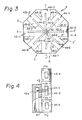
- Figure 3 is a plane view of the power distributor 4.
- the broken lines in Fig. 3 show elements of the distributor 4, taken along the line H o -Ho in Fig. 4.
- Figure 4 is a partially sectional side view of the power distributor 4, taken in the direction of an arrow A in Fig. 3.
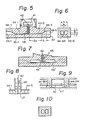
- Figure 5 is a sectional view of the power distributor 4, taken along the line X-X' shown in Fig. 3.
- Figure 6 is a sectional view of a channel provided with a ridge of the power distributor 4, taken along the line R-R' shown in Fig. 3.
- Figure 7 is a sectional view of a center portion of the power distributor 4, taken along the line Z-Z' of Fig. 3.
- the power distributor has eight distributing channels 45-1 to 45-8.
- An input microwave signal to be amplified propagates along in an input waveguide 41 and is applied to an antenna 42a of one end of an internal conductor 42 in a coaxial line path. Accordingly, the signal applied at the antenna 42a is converted into a coaxial mode.
- the other end of the inner conductor 42 in the coaxial line path is supported by a base 47 so that the inner conductor 42 is installed coaxially and spaced from a cylindrical inner wall 48 of a conductor.
- a dielectric or air is inserted between an outer conductor (the inner wall) 48 of the coaxial line path and the inner conductor 42.
- the microwave signal converted into the coaxial mode at the antenna 42a propagates with a transverse electromagnetic (TEM) mode in a path between the inner conductor 42 in the coaxial line path and the inner wall 48.
- the TEM mode signal consists of a transverse electric field and a transverse magnetic field.
- the TEM mode signal reaches the base 47.
- the power distributor 4 includes eight ridge distributing paths 44-1 to 44-8 facing the base 47 at a predetermined distance and radially formed at equal angles relative to and in a plane perpendicular to the inner conductor 42.
- a longitudinal and sectional view of the ridge distributing paths is shown in Fig. 5:
- a front sectional view of one of the ridge distributing paths is shown in Fig. 6.
- the ridge distributing paths 44-1 to 44-8 form part of the inner wall at one end and have inclined portions 46-1 to 46-8 at the other end.
- each of the ridge distributing paths 44-1 to 44-8 forms a ridge line in each of rectangular waveguides 49-1 to 49-8 each having a width a, and height b.
- the ridges terminate at the inclined portions 46-1 to 46-8.
- the ridge distributing paths 44-1 to 44-8 have the same construction and are spaced at equal angles in the radial direction.
- the microwave signal propagated with the TEM mode in the coaxial line path to the other end (the bottom) of the inner conductor 42 is equally distributed at spaces between one of the ends of the ridge distributing paths 44-1 to 44-8 adjacent to the inner conductor 42 and the base 47.
- Each of the equally distributed microwave signals at the ends of the ridge distributing paths 44-1 to 44-8 propagates radially with a ridge line mode (TEM mode) in the gap defined by the ridge and the base 47 to each of the inclined portions 46-1 to 46-8.
- the ridge distributing paths function as electric field concentration means.
- Each of the microwave signals reaching the inclined portions 46-1 to 46-8 is further introduced to the waveguides 49-1 to 49-8.
- the gradients of the inclined portions 46-1 to 46-8 are the same and designed to smoothly propagate the microwave signals reaching the other ends of the ridge distributing paths 44-1 to 44-8 to the waveguides 49-1 to 49-8. Strictly speaking, there is a partial radial mode of the propagation in the vicinity of the other end of the inner conductor 42 supported in the base 47.
- the individual semiconductor amplifiers 6 are connected to the outputs of the waveguides 49-1 to 49-8 in the power distributor.
- the power synthesizer 5 follows the amplifiers.
- the microwave signal input at the antenna 42a propagates in the coaxial line path and is equally distributed at the one ends of the ridge distributing paths 44-1 to 44-8.
- the distributed microwave signals are smoothly introduced into the waveguides 49-1 to 49-8.
- the power loss of a microwave signal propagating in the waveguide is considerably smaller than that in the coaxial cable, because the waveguide has large cross section and no dielectric loss.
- Figure 9 is a sectional view of the power distributor shown in Fig. 3, taken along the line Q-Q'.
- a normal mode there is no unnecessary electric field between the two ridges 44-2R and 44-3R liable to adversely affect the propagation of the microwave.
- an electric field may be caused by reflection due to the unbalanced load impedance in the circumferential direction of the power distributor. The electric field gives the polarity between the ridges 44-2R and 44-3R as shown. The difference of the potential between the ridges 44-2R and 44-3R would have an adverse effect on the propagation of the microwave.
- the arrows indicate the direction of the electric field.
- the resistance films 52 between the tips of the ridges and parallel to the direction of the electric field.
- the resistance films 52 absorb the unnecessary electric field and equalize the potentials between the ridges. Consequently, no electric field appears between the ridges. In this regard, it should be noted that, even in the normal mode, the resistance films 52 do not adversely influence the microwave signal.
- the resistance films 52 are provided in every gap between the tips of the ridges, however, they can be symmetrically provided concerning the coaxial inner conductor 42.
- the resistance film is formed by, e.g., vapor deposition of the resistance material on a mica film, vapor deposition of nickel-chrome (Ni-Cr) on a dielectric film, or vapor deposition of nitrogen-tantalum on a dielectric film.
- provision of a resistance film between the ridges enables elimination of an unnecessary electric field, further reducing the power loss, and at the same time improving the nature of the distributed and propagating microwave signals.
- the size of the power distributor is decided by the characteristic impedance and other parameters.
- the following are the actual dimensions of the power distributor 4 used for the 30 GHz band:
- the gap between the ridge and the base is 0.25 mm
- the length I, of the inclined portion is greater than M4 (where ⁇ : the wavelength of the microwave signal)
- the length of the ridge 1 0 is approximately 22.5 mm.
- Figure 10 is an alternative embodiment of the ridge shown in Fig. 6.
- Fig. 10 there are two ridges facing each other. The microwave propagates in the gap between the ridges.
- the input waveguide 41 shown in Figs. 4 and 5 is not essential to the present invention and may be, for example a transmission line of a microwave integrated circuit (MIC) or a normal coaxial line path.
- MIC microwave integrated circuit
- the power distributor 4 mentioned above can also be used for the power synthesizer 5, since a combined output of the microwave signal can be obtained at the antenna 42a, when microwave signals with the same phase and amplitude are input to one of the ends of the waveguides 49-1 to 49-8.
- a power synthesizer 5 of the same construction as the power distributor 4 mentioned above features high performance and reduced power loss of the microwave signal. The same applies to the other embodiments of the power distributor described hereinbelow.
- the power distributor and/or the power synthesizer can be used not only in the microwave power amplifying apparatus but also as independent devices.
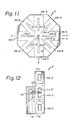
- Figure 11 is a sectional view of the power distributor, taken along the line H o ⁇ H' o shown in Fig. 12.
- Figure 12 is a side view of the power distributor, taken in the direction of an arrow A.
- Figure 13 is a sectional view of a part of the power distributor shown in Fig. 11, taken along the line X-X'.
- the power distributor 4' shown in Figs. 11 to 13 is similar to the power distributor 4 shown in Figs. 3 to 10, however, the ridge distributing paths 44-1' to 44-8' have two inclined portions 46-1 to 46-8 and 50-1 to 50-8 (Fig. 13).
- the second inclined portions 50-1 to 50-8 define a space 51 in a vicinity of the bottom end of the inner conductor 42.
- the section of the ridge distributing paths taken along the line R-R' in Fig. 11 is similar to that shown in Fig. 6.
- the microwave signal with the TEM mode reaching the space 51 along the inner conductor 42 is once converted into a radial mode.
- the converted signal is equally distributed and smoothly introduced into gaps between the ridges 44-1 R' to 44-8R' and the base 47 through the inclined portions 50-1 to 50-8.
- the microwave signals introduced in the gaps propagate with the ridge line mode and travel to waveguides 49-1 to 49-8 through the inclined portions 46-1 to 46-8, which can smoothly diffuse the microwave signals. Due to the provision of the inclined portions 50-1 to 50-8 in the power distributor 4', the power loss of the microwave is further reduced from that of the power distributor 4 of the first embodiment.
- the gap between the ridge and the base is 0.25 mm
- the height of the space 51 is less than ⁇ /4, preferably less than A/6, e.g., 1.5 mm
- the length of the inner inclined portions 50-1 to 50-8 is more than A/4
- the length of the outer inclined portions 46-1 to 46-8 is more than A/4.
- Other dimensions are same as those of the previous embodiment.
- Two ridges can be provided facing each other in the power distributor 4', as shown in Fig. 10. Also, the ridge can be formed on the side of the base 47 instead of the upper side.
- Figure 14 is a sectional view of the power distributor 4" along with individual semiconductor amplifiers 55-1 to 55-8.
- the construction and the shape of the coaxial line path, dielectric 43, inner conductor 42, inner wall 48, and space 51 are similar to those mentioned above.
- Ridges 44-1 R" to 44-8R" of the distributing paths have inner inclined portions 54-1 to 54-8 similar to those as shown in Fig. 13, however, have no outer inclined portions.
- Individual semiconductor amplifiers 55-1 to 55-8 are inserted into gaps between the base 47 and outer ends of the ridges 44-1 R" to 44-8R". On each of the amplifiers is formed a micro-strip line 55b.
- the micro-strip line 55b is one of the transmission lines of a microwave integrated circuit (MIC) formed on a dielectric substrate 55a, as shown in Fig. 15.
- Figure 15 is a plane view of one amplifier.
- One end 55c of the micro-strip line 55b is in contact with the outer end of the ridge, whereby an equally distributed microwave signal is directly introduced into the MIC transmission line and amplified in the amplifier.
- MIC microwave integrated circuit
- a construction with no inner inclined ridge portions can be also provided.
- Figure 16 is a sectional view of the power distributor 4"', taken along the line H o -Ho shown in Fig. 17.
- Figure 17 is a side sectional view of the power distributor shown in Fig. 16, taken along the line Y-Y'.
- Figure 18 is a side view of the power distributor shown in Fig. 16, taken in the direction of an arrow B.
- the power distributor 4"' consists of a coaxial line path 402 and eight waveguides 405-1 to 405-8 circumferentially positioned from the coaxial line path 402 and spaced at equal angles.
- a cylindrical space 411 is defined around the coaxial line path 402.
- the waveguides 405-1 to 405-8 directly distribute the microwave signal.
- the microwave signal input to one end of the coaxial line path 402 propagates with a coaxial mode along with the coaxial line path 402.
- the microwave signal reaching the cylindrical space 411 is converted to a radial mode and equally distributed in the waveguides 405-1 to 405-8.
- Each of the distributed microwave signals in the waveguides 405-1 to 405-8 propagates with a normal transverse electric mode in each of the waveguides.
- the power loss of a microwave of higher-than X band frequency in the power distributor 4"' is smaller than that of a power distributor using a coaxial cables.
- wedge portions 406-1 to 406-8 each of which has an acute angle tip for convergence of the electric field of the microwave signal, as joint portions of neighboring waveguides.
- These wedge portions can reflect part of the microwave signals, which could have a detrimental effect on the power distribution, such as the phase characteristic, and might increase the power loss.
- Various type of wedges able to overcome this problem will be described below with reference to Figs. 19 to 22.
- FIG. 19(A) is a front view of the wedge
- Fig. 19(B) a plane view
- Fig. 19(C) a side view.
- the wedge has a gradient 406a having a length 1 0 which is equal or greater than A/4, where ⁇ is the wavelength of the microwave signal.
- the microwave signal is still reflected on the surface of the gradient 406a, however, an incident and the reflected waves have a phase difference of 180° due to the shape of the gradient 406a. Therefore, the two reflected waves are cancelled, and the effect of the reflection is negligible.
- the wedges shown in Figs. 19 to 22 function to eliminate any adverse effect of reflection as with the wedge 406 shown in Fig. 16.
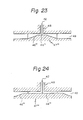
- FIG. 23 is a sectional view of the power distributor.
- the power distributor includes a coaxial line path including an inner conductor 42 and an inner wall 48 of a conductor, a base 47"' having a center flat portion 44'" and an inclined portion 46"', and waveguide 49.
- the radial line portions of the prior embodiments are made level so as to reduce the generation of the higher mode electric field at a transition part of the coaxial line path and the radial line path.
- the inclined portion 46'" introduces the microwave signal into the waveguides smoothly, and the microwave signal is distributed in the waveguides.
- the length of the inclined portion 46'" is, preferably, greater than A/4.
- the inclined portion can be replaced by a plurality of steps.
- FIG. 24 s a sectional view of a power distributor similar to that of the power distributor shown in Fig. 23.
- a base 17"" forms a center flat portion 44"" greater than that shown in Fig. 23 and an inclined portion 46"".
- the microwave signal is equally distributed in a gap between the center flat portion 14"" and an upper flat portion facing the flat portion 44"". The distributed signals are introduced to the waveguides 49.
- the features of the power distributor shown in Fig. 24 are similar to those of the power distributor shown in Fig. 23.
- the same modifications of shape of the power distributor shown in Fig. 23 apply to the power distributor shown in Fig. 24.
- Figure 25 is a plane sectional view of the power distributor.
- Figure 26 is a side sectional view of the power distributor.
- the power distributor has a coaxial line path 422, circumferentially positioned waveguides 425, nner walls 426 having holes 427, and a cylindrical cavity 429 defined by the inner walls 426.
- the microwave signal propagated in the cavity 429 is changed to a radial mode and is equally distributed and introduced nto the waveguides 425 through each of the holes 427.
- the holes 427 have the same dimensions and are positioned at equal distances.
- the semiconductor amplifiers are provided following the waveguides.
- dielectric members 420 are inserted into the holes 427, as shown by a broken line in Fig. 26.
- the dielectric members converge the microwave signal at the tip facing the cavity to reduce the reflection.
- Two examples of the dielectric members are shown in Figs. 27 and 28.
- the first dielectric member shown in Fig. 27 is a multifaceted double cone, while the second member shown in Fig. 28 is a double circular cone.
- the holes 427 are made so the dielectric members can fit therein.
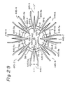
- FIG. 29 is a plane sectional view of the power distributor.
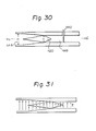
- Figure 30 is a partial side sectional view.
- the power distributor includes a vessel 51 having apertures 511-1 to 511-8 positioned at equal distances and defining a cavity 449, a coaxial line path 442, and waveguides 445-1 to 445-8.
- the waveguides 445-1 to 145-8 have tapered portions 445-1 a to 445-8a, each of which is connected to the aperture of the vessel 51.
- the microwave signal propagated at the cavity 449 with the TEM mode is converted to a radial mode and is equally distributed and introduced into the waveguides 445-1 to 445-8 through the apertures 511-1 to 511-8, as shown in Fig. 31.
- a plurality of waveguides i.e., the power distributing paths, can be radially provided rather than the above-mentioned distributor.
- dielectric members 420-1 to 420-8 for example, as shown in Figs. 27 and 28, are inserted into apertures 511-1 to 511-8.
- the microwave signal with the radial mode in the cavity 449 is equally concentrated on tips each having a sharp shape, of the dielectric members 420-1 to 420-8.
- the trapped electric field of the microwave signals propagate in the dielectric members and are introduced into the waveguides. Consequently, the power loss is minimized, and the power distribution, phase, and amplitude can be improved.
- the size of the aperture for connecting the cavity 49 and the waveguides 445-1 to 445-8 is considerably reduced. This means the joint portion are smaller than those of not only conventional power distributors but also the embodiments of power distributors shown in Figs. 16 to 24.
- the cavity-side length of the dielectric member is approximately ⁇ /8 to ⁇ /2 and the waveguide-side length is greater than ⁇ /4.
- the actual dimensions of the power distributor for 30 GHz with dielectric members having a specific inductive capacity of 10 are as follows:
- the microwave power amplifying apparatus can consist of any one of the above-mentioned power distributors, a plurality of semiconductor amplifiers, and anyone of the above-mentioned power synthesizers.
- the microwave power amplifying apparatus may comprise a ridge-distributing-path-type power distributor and a waveguide-type power synthesizer.
Landscapes
- Engineering & Computer Science (AREA)
- Power Engineering (AREA)
- Microwave Amplifiers (AREA)
- Amplifiers (AREA)
Claims (21)
Applications Claiming Priority (2)
| Application Number | Priority Date | Filing Date | Title |
|---|---|---|---|
| JP125533/83 | 1983-07-12 | ||
| JP58125533A JPS6018007A (ja) | 1983-07-12 | 1983-07-12 | マイクロ波電力増幅装置 |
Publications (2)
| Publication Number | Publication Date |
|---|---|
| EP0135407A1 EP0135407A1 (de) | 1985-03-27 |
| EP0135407B1 true EP0135407B1 (de) | 1988-03-30 |
Family
ID=14912539
Family Applications (1)
| Application Number | Title | Priority Date | Filing Date |
|---|---|---|---|
| EP84401431A Expired EP0135407B1 (de) | 1983-07-12 | 1984-07-05 | Anordnung zur Verteilung und Zusammenführung von Mikrowellenenergie und damit aufgebauter Mikrowellenleistungsverstärker |
Country Status (5)
| Country | Link |
|---|---|
| US (1) | US4598254A (de) |
| EP (1) | EP0135407B1 (de) |
| JP (1) | JPS6018007A (de) |
| CA (1) | CA1223049A (de) |
| DE (1) | DE3470264D1 (de) |
Families Citing this family (25)
| Publication number | Priority date | Publication date | Assignee | Title |
|---|---|---|---|---|
| US4673899A (en) * | 1985-09-23 | 1987-06-16 | General Electric Company | H-plane stacked waveguide power divider/combiner |
| JPS62196266A (ja) * | 1986-02-20 | 1987-08-29 | Toray Ind Inc | 糸条の巻取装置 |
| JPH0733206B2 (ja) * | 1986-02-20 | 1995-04-12 | 東レ株式会社 | 糸条巻取装置 |
| US4724400A (en) * | 1987-04-21 | 1988-02-09 | Trw Inc. | Linear amplifier assembly |
| GB2226201B (en) * | 1988-12-01 | 1992-09-30 | Ferranti Int Signal | Microwave power amplifying arrangement |
| US5128628A (en) * | 1990-12-26 | 1992-07-07 | Sgs-Thomson Microelectronics, Inc. | Solid state high power amplifier module |
| JPH05191178A (ja) * | 1992-01-16 | 1993-07-30 | Japan Radio Co Ltd | 電力増幅装置 |
| US6242984B1 (en) * | 1998-05-18 | 2001-06-05 | Trw Inc. | Monolithic 3D radial power combiner and splitter |
| GB2347793A (en) * | 1999-03-09 | 2000-09-13 | Isis Innovation | Degenerate mode combiner |
| US6730038B2 (en) * | 2002-02-05 | 2004-05-04 | Tensys Medical, Inc. | Method and apparatus for non-invasively measuring hemodynamic parameters using parametrics |
| US7385462B1 (en) * | 2005-03-18 | 2008-06-10 | The United States Of America As Represented By The Administrator Of The National Aeronautics And Space Administration | Wideband radial power combiner/divider fed by a mode transducer |
| FR2925230B1 (fr) * | 2007-12-18 | 2009-12-04 | Thales Sa | Dispositif d'amplification de puissance radiale a compensation de dispersion de phase des voies amplification |
| US8508313B1 (en) | 2009-02-12 | 2013-08-13 | Comtech Xicom Technology Inc. | Multiconductor transmission line power combiner/divider |
| CN101826648B (zh) * | 2009-03-04 | 2013-02-06 | 中国科学院微电子研究所 | 基于波导的功率合成器 |
| CN103219574B (zh) * | 2012-01-19 | 2014-12-17 | 中国电子科技集团公司第十研究所 | 毫米波超宽带空间功率合成网络 |
| US9793593B1 (en) | 2015-03-30 | 2017-10-17 | David B. Aster | Power combiners and dividers including cylindrical conductors and capable of receiving and retaining a gas |
| US9947986B1 (en) | 2015-03-30 | 2018-04-17 | David B. Aster | Reactive power combiners and dividers including nested coaxial conductors |
| US9812756B1 (en) | 2015-03-30 | 2017-11-07 | David B. Aster | Systems and methods for combining or dividing microwave power using satellite conductors and capable of receiving and retaining a gas |
| US9960469B1 (en) | 2015-03-30 | 2018-05-01 | David B. Aster | Broadband reactive power combiners and dividers including nested coaxial conductors |
| US10312565B1 (en) | 2015-03-30 | 2019-06-04 | David B. Aster | Microwave power divider/combiner devices, microwave power divider/combiner bandpass filters, and methods of thermally cooling a cable run |
| US9673503B1 (en) | 2015-03-30 | 2017-06-06 | David B. Aster | Systems and methods for combining or dividing microwave power |
| JP2017076881A (ja) * | 2015-10-15 | 2017-04-20 | 新日本無線株式会社 | 電力合成・分配器 |
| JP6811995B2 (ja) * | 2017-04-17 | 2021-01-13 | 国立研究開発法人理化学研究所 | 高周波電力増幅装置 |
| US12272858B2 (en) * | 2022-11-21 | 2025-04-08 | Raytheon Company | Ridged N-way coaxial vacuum power combiner signal injector with radial feeds usable in a coaxial vacuum-electron device |
| US12283738B2 (en) * | 2022-11-21 | 2025-04-22 | Raytheon Company | N-way coaxial signal injector with axial feeds |
Family Cites Families (14)
| Publication number | Priority date | Publication date | Assignee | Title |
|---|---|---|---|---|
| US2550524A (en) * | 1945-08-20 | 1951-04-24 | Rca Corp | Balanced microwave detector |
| NL160530B (nl) * | 1951-04-14 | Secretary Trade Ind Brit | Passieve anti-slingertank. | |
| US3001160A (en) * | 1959-07-20 | 1961-09-19 | John E Trousdale | High pressure waveguide window |
| US3290682A (en) * | 1964-11-02 | 1966-12-06 | Hughes Aircraft Co | Multiple beam forming antenna apparatus |
| US3582813A (en) * | 1969-06-19 | 1971-06-01 | Microwave Ass | Negative-resistance multiple-element combiner |
| US3873935A (en) * | 1974-05-13 | 1975-03-25 | Hughes Aircraft Co | Microwave power accumulation structures comprising a plurality of stacked elliptical cavities |
| US3986188A (en) * | 1974-09-09 | 1976-10-12 | Litton Systems, Inc. | Dual mode microwave amplifier subsystem |
| US4035746A (en) * | 1976-09-07 | 1977-07-12 | The Bendix Corporation | Concentric broadband power combiner or divider |
| US4175257A (en) * | 1977-10-05 | 1979-11-20 | United Technologies Corporation | Modular microwave power combiner |
| US4188590A (en) * | 1977-11-25 | 1980-02-12 | Hughes Aircraft Company | Conical power combiner |
| US4147994A (en) * | 1978-07-31 | 1979-04-03 | Raytheon Company | Power combiner |
| JPS55147011A (en) * | 1979-05-04 | 1980-11-15 | Mitsubishi Electric Corp | Microwave amplifier |
| US4238747A (en) * | 1979-08-10 | 1980-12-09 | The United States Of America As Represented By The Secretary Of The Air Force | Mode filter apparatus |
| DE3202711C2 (de) * | 1982-01-28 | 1983-12-22 | Siemens AG, 1000 Berlin und 8000 München | Mikrowellen-Verstärkereinrichtung |
-
1983
- 1983-07-12 JP JP58125533A patent/JPS6018007A/ja active Pending
-
1984
- 1984-06-27 CA CA000457606A patent/CA1223049A/en not_active Expired
- 1984-07-05 EP EP84401431A patent/EP0135407B1/de not_active Expired
- 1984-07-05 DE DE8484401431T patent/DE3470264D1/de not_active Expired
- 1984-07-12 US US06/630,240 patent/US4598254A/en not_active Expired - Fee Related
Also Published As
| Publication number | Publication date |
|---|---|
| EP0135407A1 (de) | 1985-03-27 |
| DE3470264D1 (en) | 1988-05-05 |
| CA1223049A (en) | 1987-06-16 |
| US4598254A (en) | 1986-07-01 |
| JPS6018007A (ja) | 1985-01-30 |
Similar Documents
| Publication | Publication Date | Title |
|---|---|---|
| EP0135407B1 (de) | Anordnung zur Verteilung und Zusammenführung von Mikrowellenenergie und damit aufgebauter Mikrowellenleistungsverstärker | |
| US4291278A (en) | Planar microwave integrated circuit power combiner | |
| AU2006220545B2 (en) | Method and apparatus for increasing performance in a waveguide-based spatial power combiner | |
| US4527165A (en) | Miniature horn antenna array for circular polarization | |
| JP2951707B2 (ja) | 平面アンテナ | |
| US4641107A (en) | Printed circuit radial power combiner with mode suppressing resistors fired at high temperature | |
| US5010348A (en) | Device for exciting a waveguide with circular polarization from a plane antenna | |
| US4677393A (en) | Phase-corrected waveguide power combiner/splitter and power amplifier | |
| US5600286A (en) | End-on transmission line-to-waveguide transition | |
| US20130120086A1 (en) | Compact omt device | |
| EP0423114B1 (de) | Mikrowellenmultiplexer mit mehrmodenfilter | |
| US4641106A (en) | Radial power amplifier | |
| JP2004535131A (ja) | 2個の放射要素を備えるリアクティブ結合アンテナ | |
| KR100897864B1 (ko) | 커플링을 이용한 전력 분배기 | |
| EP0417205B1 (de) | Hochleistungsausgangsschaltkreis mit verlängerter wechselwirkung | |
| GB2222489A (en) | Waveguide apparatus | |
| RU2083035C1 (ru) | Высокочастотная плоская антенная решетка | |
| US20040032374A1 (en) | Compact wide scan periodically loaded edge slot waveguide array | |
| JPH0746011A (ja) | 電力分配器 | |
| JPH04233802A (ja) | ストリップ線路マイクロ波モジュール | |
| JP3976004B2 (ja) | T分岐導波管、およびアレーアンテナ | |
| KR20010112034A (ko) | 도파관-마이크로스트립 변환 구조를 이용한 전력 결합기 | |
| JP4972041B2 (ja) | フィルタ | |
| EP0357233A2 (de) | Wellenleitergerät | |
| JPH07202558A (ja) | 平面アンテナ |
Legal Events
| Date | Code | Title | Description |
|---|---|---|---|
| PUAI | Public reference made under article 153(3) epc to a published international application that has entered the european phase |
Free format text: ORIGINAL CODE: 0009012 |
|
| AK | Designated contracting states |
Designated state(s): DE FR GB IT NL |
|
| 17P | Request for examination filed |
Effective date: 19850420 |
|
| 17Q | First examination report despatched |
Effective date: 19860729 |
|
| GRAA | (expected) grant |
Free format text: ORIGINAL CODE: 0009210 |
|
| AK | Designated contracting states |
Kind code of ref document: B1 Designated state(s): DE FR GB IT NL |
|
| REF | Corresponds to: |
Ref document number: 3470264 Country of ref document: DE Date of ref document: 19880505 |
|
| ITF | It: translation for a ep patent filed | ||
| ET | Fr: translation filed | ||
| PLBE | No opposition filed within time limit |
Free format text: ORIGINAL CODE: 0009261 |
|
| STAA | Information on the status of an ep patent application or granted ep patent |
Free format text: STATUS: NO OPPOSITION FILED WITHIN TIME LIMIT |
|
| 26N | No opposition filed | ||
| ITTA | It: last paid annual fee | ||
| PGFP | Annual fee paid to national office [announced via postgrant information from national office to epo] |
Ref country code: GB Payment date: 19930505 Year of fee payment: 10 |
|
| PGFP | Annual fee paid to national office [announced via postgrant information from national office to epo] |
Ref country code: FR Payment date: 19930729 Year of fee payment: 10 |
|
| PGFP | Annual fee paid to national office [announced via postgrant information from national office to epo] |
Ref country code: NL Payment date: 19930731 Year of fee payment: 10 |
|
| PGFP | Annual fee paid to national office [announced via postgrant information from national office to epo] |
Ref country code: DE Payment date: 19930917 Year of fee payment: 10 |
|
| PG25 | Lapsed in a contracting state [announced via postgrant information from national office to epo] |
Ref country code: GB Effective date: 19940705 |
|
| PG25 | Lapsed in a contracting state [announced via postgrant information from national office to epo] |
Ref country code: NL Effective date: 19950201 |
|
| GBPC | Gb: european patent ceased through non-payment of renewal fee |
Effective date: 19940705 |
|
| NLV4 | Nl: lapsed or anulled due to non-payment of the annual fee | ||
| PG25 | Lapsed in a contracting state [announced via postgrant information from national office to epo] |
Ref country code: FR Effective date: 19950331 |
|
| PG25 | Lapsed in a contracting state [announced via postgrant information from national office to epo] |
Ref country code: DE Effective date: 19950401 |
|
| REG | Reference to a national code |
Ref country code: FR Ref legal event code: ST |