EP0135672A1 - Ausgleichsschaltung für in Reihe geschaltete Schalter - Google Patents
Ausgleichsschaltung für in Reihe geschaltete Schalter Download PDFInfo
- Publication number
- EP0135672A1 EP0135672A1 EP84106109A EP84106109A EP0135672A1 EP 0135672 A1 EP0135672 A1 EP 0135672A1 EP 84106109 A EP84106109 A EP 84106109A EP 84106109 A EP84106109 A EP 84106109A EP 0135672 A1 EP0135672 A1 EP 0135672A1
- Authority
- EP
- European Patent Office
- Prior art keywords
- switches
- balancing
- series
- windings
- capacitors
- Prior art date
- Legal status (The legal status is an assumption and is not a legal conclusion. Google has not performed a legal analysis and makes no representation as to the accuracy of the status listed.)
- Granted
Links
Images

Classifications
-
- H—ELECTRICITY
- H02—GENERATION; CONVERSION OR DISTRIBUTION OF ELECTRIC POWER
- H02M—APPARATUS FOR CONVERSION BETWEEN AC AND AC, BETWEEN AC AND DC, OR BETWEEN DC AND DC, AND FOR USE WITH MAINS OR SIMILAR POWER SUPPLY SYSTEMS; CONVERSION OF DC OR AC INPUT POWER INTO SURGE OUTPUT POWER; CONTROL OR REGULATION THEREOF
- H02M3/00—Conversion of DC power input into DC power output
- H02M3/02—Conversion of DC power input into DC power output without intermediate conversion into AC
- H02M3/04—Conversion of DC power input into DC power output without intermediate conversion into AC by static converters
- H02M3/10—Conversion of DC power input into DC power output without intermediate conversion into AC by static converters using discharge tubes with control electrode or semiconductor devices with control electrode
- H02M3/145—Conversion of DC power input into DC power output without intermediate conversion into AC by static converters using discharge tubes with control electrode or semiconductor devices with control electrode using devices of a triode or transistor type requiring continuous application of a control signal
- H02M3/155—Conversion of DC power input into DC power output without intermediate conversion into AC by static converters using discharge tubes with control electrode or semiconductor devices with control electrode using devices of a triode or transistor type requiring continuous application of a control signal using semiconductor devices only
- H02M3/156—Conversion of DC power input into DC power output without intermediate conversion into AC by static converters using discharge tubes with control electrode or semiconductor devices with control electrode using devices of a triode or transistor type requiring continuous application of a control signal using semiconductor devices only with automatic control of output voltage or current, e.g. switching regulators
- H02M3/158—Conversion of DC power input into DC power output without intermediate conversion into AC by static converters using discharge tubes with control electrode or semiconductor devices with control electrode using devices of a triode or transistor type requiring continuous application of a control signal using semiconductor devices only with automatic control of output voltage or current, e.g. switching regulators including plural semiconductor devices as final control devices for a single load
Definitions
- the invention relates to a device for balancing switches connected in series between a voltage source and a load, each switch being connected in parallel with a balancing capacitor and a diode.
- Electronic switches used for the production of electrical energy converters such as, for example, shakers or inverters, are usually made by means of semiconductor components such as thyristors, transistors, or thyristors lockable by the trigger.
- the highest voltage that the semiconductor components can withstand is currently limited to a few hundred volts for the transistors and a few thousand volts for the thyristors and the lockable thyristors.
- the preferred field of application of the device according to the invention is that of the series connection of lockable transistors or thyristors.
- the first drawback is that the balancing of the voltages between the two switches is not perfectly ensured because the capacitor associated with the switch, the opening of which takes place with the lowest delay, charges more than the capacitor associated the switch which opens with the greatest delay. This results in an increase in the voltage withstand required for the switches.
- the second drawback is that, in order to keep the imbalance within acceptable limits, it is necessary to use capacitors of relatively large value.
- the energy stored in these capacitors is therefore relatively high and as it is dissipated in the resistors each time the switches are closed, this causes a reduction in the efficiency and cooling difficulties of the electrical energy converter using this arrangement.
- the device according to the invention makes it possible to improve the voltage balancing of blockable transistors or thyristors connected in series without any sorting being necessary and with a reduction in losses compared with known arrangements.
- the device according to the invention is characterized in that it comprises a transformer provided with windings, each winding being connected in parallel with a switch and in series with a diode, so that the electrical energy initially stored in the capacitors d balancing is, when the switches are closed, stored as magnetic energy in the windings, then reused, when the switches are opened, to accelerate the recharging of the least charged capacitors until the voltage is reached of the most charged capacitor.
- the capacitors being connected in parallel with the switches, this ensures voltage balancing of the switches.
- the remaining magnetic energy surplus, after the balancing capacitors have recharged, is returned to the power source.
- this device comprises two switches, but it) could include at least three switches on which are connected in parallel at least three windings forming part of a single trisformer.
- the device can be applied to the production of an inverter in which each half-phase 3 is constituted by switches in series.
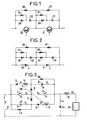
- the switches of this prior device are transistors 30, 31 to which are connected in parallel, and respectively, capacitors 32, 33 of extremely large value.
- the energy stored in these capacitors is therefore relatively high and each time these switches are closed, this energy is dissipated in resistors 34, 35 respectively.
- the switches of this prior device are blockable thyristors 40, 41 to which are connected in parallel and respectively capacitors 42, 43.
- the switches 4, 11 can be either transistors or blockable thyristors, and the device comprises the following elements: two capacitors 2 and 9 of equal values, a transformer 20 comprising two windings 6 and 13 whose resistance ohmic is assumed to be negligible, comprising the same number of turns, and assumed to be perfectly coupled, two diodes 7 and 8 assumed to be perfect, two resistors 3 and 10 of equal values, intended to ensure static balancing of the voltages between the switches 4 and 11, two diodes 5 and 12 assumed to be perfect, intended to prevent the presence of the windings 6 and 13 from disturbing the static balancing of the voltages between the capacitors 2 and 9.
- the device in FIG. 3 represents a voltage chopper, and this device operates in the following manner.
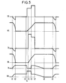
- FIGS. 4 and 5 represent the variations as a function of time of the different currents and voltages, in order to monitor the operation of this device according to the invention.
- the capacitors 2 and 9 then begin to discharge, causing the appearance of a current I 2 through the elements 4, 11, 13, 12 with regard to the capacitor 2 and causing the appearance of a current I 9 through elements 6, 5, 4 and 11 with regard to capacitor 9.
- the capacitors 2 and 9 are completely discharged. They transmitted their energy to winding 13 with regard to capacitor 2 and to winding 6 with regard to capacitor 9. This energy is stored in the form of magnetic energy and is manifested by the presence of a current I 6 flowing through the elements 5, 4 and 8 with regard to the winding 6 and by the presence of a current I 13 flowing through the elements 12, 7, 11 with regard to the winding 13.
- windings 6 and 13 having the same number of turns, the. currents I 6 and I 13 are equal to each other.
- the switch 11 opens in turn and the current I 11 equal to I 15 + I13 which passed through it, is interrupted. This current is derived by the capacitor 9 which begins to charge.
- the voltage across the winding 13 may increase since the winding 6 to which it is coupled is not short-circuited by the switch 4 open from time t 4 .
- the diode 12 therefore remains conductive and the current I 13 continues to flow through the elements 13, 12, 7 and 8.
- the capacitor 9 is therefore charged by a current equal to I 15 + I 13 .
- the magnetic energy stored in the winding 13 and which is equal, assuming negligible losses, to the sum of the energies stored in the windings 6 and 13 at time t 3 , therefore serves to start from the instant t 5 to accelerate the recharging of the capacitor 9 with respect to the recharging of the capacitor 2.
- the diode 14 therefore becomes conductive again and then drifts the current I 15 which ceases to charge the capacitors 2 and 9.
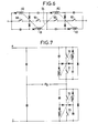
- FIG. 6 represents the device according to the invention applied to the series connection of four switches 50, 51, 52, 53.
- the windings 60, 61, 62, 63 all have the same number of turns and are coupled together in being arranged on a single magnetic circuit, for example, a transformer 64.
- Static balancing resistors, not shown, are each in parallel on a capacitor or on a switch.
- FIG. 7 represents the device according to the invention, applied to the production of a single-phase inverter comprising in each half-phase two switches connected in series 70, 71; 72 ,. 73.
- Static balancing resistors are each in parallel on a capacitor or on a switch.
- this device can extend, on the one hand to any number, but preferably even, of switches connected in series, on the other hand, to all applications requiring the use switches connected in series.
Landscapes
- Power Engineering (AREA)
- Engineering & Computer Science (AREA)
- Direct Current Feeding And Distribution (AREA)
- Power Conversion In General (AREA)
- Details Of Garments (AREA)
- Transplanting Machines (AREA)
- Inverter Devices (AREA)
- Testing Of Balance (AREA)
- Lift-Guide Devices, And Elevator Ropes And Cables (AREA)
- Electrophonic Musical Instruments (AREA)
- Interface Circuits In Exchanges (AREA)
- Constituent Portions Of Griding Lathes, Driving, Sensing And Control (AREA)
- Bakery Products And Manufacturing Methods Therefor (AREA)
- Dc-Dc Converters (AREA)
- Networks Using Active Elements (AREA)
- Keying Circuit Devices (AREA)
- Electronic Switches (AREA)
- Protection Of Static Devices (AREA)
- Charge And Discharge Circuits For Batteries Or The Like (AREA)
- Rectifiers (AREA)
Priority Applications (1)
| Application Number | Priority Date | Filing Date | Title |
|---|---|---|---|
| AT84106109T ATE34259T1 (de) | 1983-05-30 | 1984-05-29 | Ausgleichsschaltung fuer in reihe geschaltete schalter. |
Applications Claiming Priority (2)
| Application Number | Priority Date | Filing Date | Title |
|---|---|---|---|
| FR8308891A FR2547106B1 (fr) | 1983-05-30 | 1983-05-30 | Dispositif d'equilibrage d'interrupteurs connectes en serie |
| FR8308891 | 1983-05-30 |
Publications (2)
| Publication Number | Publication Date |
|---|---|
| EP0135672A1 true EP0135672A1 (de) | 1985-04-03 |
| EP0135672B1 EP0135672B1 (de) | 1988-05-11 |
Family
ID=9289289
Family Applications (1)
| Application Number | Title | Priority Date | Filing Date |
|---|---|---|---|
| EP84106109A Expired EP0135672B1 (de) | 1983-05-30 | 1984-05-29 | Ausgleichsschaltung für in Reihe geschaltete Schalter |
Country Status (9)
| Country | Link |
|---|---|
| US (1) | US4555754A (de) |
| EP (1) | EP0135672B1 (de) |
| JP (1) | JPS59228421A (de) |
| AT (1) | ATE34259T1 (de) |
| CA (1) | CA1207386A (de) |
| DE (1) | DE3471215D1 (de) |
| ES (1) | ES8503452A1 (de) |
| FI (1) | FI842134A7 (de) |
| FR (1) | FR2547106B1 (de) |
Cited By (1)
| Publication number | Priority date | Publication date | Assignee | Title |
|---|---|---|---|---|
| US4686393A (en) * | 1984-02-01 | 1987-08-11 | National Research Development Corporation | Circuit breakers for direct and alternating current |
Families Citing this family (20)
| Publication number | Priority date | Publication date | Assignee | Title |
|---|---|---|---|---|
| FR2579039B1 (fr) * | 1985-03-15 | 1987-06-05 | Thomson Csf | Dispositif d'aide a la commutation d'interrupteur et de diode de roue libre |
| US4674213A (en) * | 1985-04-01 | 1987-06-23 | Cliff Keithley | Extruded aluminum sign frame section |
| US4688165A (en) * | 1986-04-11 | 1987-08-18 | Rca Corporation | Current fed inverter bridge with conduction overlap and load tuning |
| US4783728A (en) * | 1986-04-29 | 1988-11-08 | Modular Power Corp. | Modular power supply with PLL control |
| US4697230A (en) * | 1986-06-23 | 1987-09-29 | Westinghouse Electric Corp. | AC power supplied static switching apparatus having energy recovery capability |
| US4691270A (en) * | 1986-07-22 | 1987-09-01 | Rca Corporation | Current fed inverter bridge with lossless snubbers |
| US4937725A (en) * | 1989-06-19 | 1990-06-26 | Sundstrand Corporation | Circuit for eliminating snubber current noise in the sense circuit of an H-bridge inverter |
| US5124629A (en) * | 1991-04-23 | 1992-06-23 | The United States Of America As Represented By The United States Department Of Energy | Post regulation circuit with energy storage |
| US5880581A (en) * | 1997-12-08 | 1999-03-09 | Yang; Tai-Her | AC or bidirectional circuit utilizing unipolar capacitors |
| DE19843692C2 (de) * | 1998-09-24 | 2003-04-30 | Aloys Wobben | Wechselrichter für die Einspeisung sinusförmiger Ströme in ein Wechselstromnetz |
| JP3280635B2 (ja) * | 1999-04-21 | 2002-05-13 | 長野日本無線株式会社 | エネルギー移送装置および蓄電システム |
| JP3280641B2 (ja) * | 1999-09-08 | 2002-05-13 | 長野日本無線株式会社 | エネルギー移送装置 |
| JP3280642B2 (ja) * | 1999-09-08 | 2002-05-13 | 長野日本無線株式会社 | 蓄電モジュール |
| TW492021B (en) * | 1999-11-05 | 2002-06-21 | Tokin Corp | Electrical energy storage provided with cell energy adjusting device and adjust method of cell energy |
| JP3795499B2 (ja) * | 2003-12-26 | 2006-07-12 | 富士重工業株式会社 | 蓄電素子の電圧均等化装置 |
| DE102005052579A1 (de) * | 2005-11-02 | 2007-05-03 | Phoenix Contact Gmbh & Co. Kg | Einkanalige sichere Schaltung für den Ausgang eines Bus-Teilnehmers |
| DE102006030448B4 (de) | 2006-06-29 | 2022-08-18 | Phoenix Contact Gmbh & Co. Kg | Sichere Ausgangsschaltung mit einem einkanaligen Peripherieanschluss für den Ausgang eines Bus-Teilnehmers |
| EP3945669A1 (de) | 2020-07-27 | 2022-02-02 | TRUMPF Huettinger Sp. Z o. o. | Hochspannungsschaltereinheit, impulsanordnung und verfahren zur vermeidung von spannungsunsymmetrien in einem hochspannungsschalter |
| EP3945541A1 (de) | 2020-07-29 | 2022-02-02 | TRUMPF Huettinger Sp. Z o. o. | Impulsanordnung, stromversorgungsanordnung und verfahren mit der verwendung der impulsanordnung |
| EP3952083A1 (de) | 2020-08-06 | 2022-02-09 | TRUMPF Huettinger Sp. Z o. o. | Hv-schalteinheit |
Citations (1)
| Publication number | Priority date | Publication date | Assignee | Title |
|---|---|---|---|---|
| US4276588A (en) * | 1979-06-22 | 1981-06-30 | Mclyman W T | Push-pull converter with energy saving circuit for protecting switching transistors from peak power stress |
Family Cites Families (5)
| Publication number | Priority date | Publication date | Assignee | Title |
|---|---|---|---|---|
| SU610269A1 (ru) * | 1977-01-10 | 1978-06-05 | Киевский Ордена Ленина Политехнический Институт Им.50-Летия Великой Октябрьской Социалистической Революции | Инвертор |
| SU881948A1 (ru) * | 1980-01-10 | 1981-11-15 | Уфимский авиационный институт им. Орджоникидзе | Устройство дл равномерного распределени напр жени между N последовательно соединенными управл емыми вентил ми |
| JPS56136173A (en) * | 1980-03-26 | 1981-10-24 | Toshiba Corp | Spanner circuit |
| JPS5836171A (ja) * | 1981-08-28 | 1983-03-03 | Toshiba Corp | トランジスタチヨツパ装置 |
| JPS5848305A (ja) * | 1981-09-17 | 1983-03-22 | 協和電線株式会社 | 防爆耐火ケ−ブル |
-
1983
- 1983-05-30 FR FR8308891A patent/FR2547106B1/fr not_active Expired
-
1984
- 1984-05-28 JP JP59108278A patent/JPS59228421A/ja active Pending
- 1984-05-28 FI FI842134A patent/FI842134A7/fi not_active Application Discontinuation
- 1984-05-29 DE DE8484106109T patent/DE3471215D1/de not_active Expired
- 1984-05-29 EP EP84106109A patent/EP0135672B1/de not_active Expired
- 1984-05-29 CA CA000455384A patent/CA1207386A/fr not_active Expired
- 1984-05-29 ES ES532912A patent/ES8503452A1/es not_active Expired
- 1984-05-29 AT AT84106109T patent/ATE34259T1/de not_active IP Right Cessation
- 1984-05-30 US US06/615,450 patent/US4555754A/en not_active Expired - Fee Related
Patent Citations (1)
| Publication number | Priority date | Publication date | Assignee | Title |
|---|---|---|---|---|
| US4276588A (en) * | 1979-06-22 | 1981-06-30 | Mclyman W T | Push-pull converter with energy saving circuit for protecting switching transistors from peak power stress |
Non-Patent Citations (1)
| Title |
|---|
| PATENTS ABSTRACTS OF JAPAN, vol. 6, no. 16, 29 janvier 1982, (E-92)(894); & JP - A - 56 136 173 (TOKYO SHIBAURA DENKI K.K.) (24.10.1981) * |
Cited By (1)
| Publication number | Priority date | Publication date | Assignee | Title |
|---|---|---|---|---|
| US4686393A (en) * | 1984-02-01 | 1987-08-11 | National Research Development Corporation | Circuit breakers for direct and alternating current |
Also Published As
| Publication number | Publication date |
|---|---|
| EP0135672B1 (de) | 1988-05-11 |
| JPS59228421A (ja) | 1984-12-21 |
| FI842134A7 (fi) | 1984-12-01 |
| DE3471215D1 (en) | 1988-06-16 |
| FR2547106A1 (fr) | 1984-12-07 |
| ATE34259T1 (de) | 1988-05-15 |
| FI842134A0 (fi) | 1984-05-28 |
| US4555754A (en) | 1985-11-26 |
| CA1207386A (fr) | 1986-07-08 |
| ES532912A0 (es) | 1985-02-01 |
| ES8503452A1 (es) | 1985-02-01 |
| FR2547106B1 (fr) | 1985-07-12 |
Similar Documents
| Publication | Publication Date | Title |
|---|---|---|
| EP0135672B1 (de) | Ausgleichsschaltung für in Reihe geschaltete Schalter | |
| EP0502067B1 (de) | Ladevorrichtung zur elektrischen energiespeicherung mit ladesteuerungsmitteln | |
| FR3097089A1 (fr) | Un convertisseur et son systeme de controle de courant | |
| FR2615016A1 (fr) | Dispositif de source d'alimentation a commutation | |
| FR2956266A1 (fr) | Dispositif convertisseur et alimentation sans interruption equipee d'un tel dispositif | |
| FR3036237A1 (fr) | Dispositif de conversion de puissance moyenne tension multiniveaux a sortie alternative | |
| CH616784A5 (de) | ||
| EP2320553B1 (de) | Stromumwandlungsvorrichtung und unterbrechungsfreie Stromversorgung, die eine solche Vorrichtung umfasst | |
| FR2529031A1 (fr) | Circuit d'alimentation pour appareil de soudage a l'arc | |
| FR2936113A1 (fr) | Dispositif convertisseur et alimentation sans interruption equipee d'un tel dispositif | |
| BE897592A (fr) | Regulateur pour charge de batterie d'accumulateurs par alternateur a aimant permanent | |
| EP0670624B1 (de) | Angepasstes Schaltnetzteil um Kommutierungen bei niedriger Spannung auszuführen | |
| EP0107539B1 (de) | Steuerschaltung für einen Synchronmotor mit zwei Ankerwicklungen | |
| EP2413485A1 (de) | System zur Einspeisung einer Wechselstromladung aus einem Alternativnetz ohne Gegenwart eines Transformators zwischen dem Netz und dem Einspeisungssystem sowie Antriebskette, die ein solches System umfasst | |
| EP0743742A1 (de) | Leistungsfaktorverbesserung für eine gleichgerichtete Leistungsversorgung | |
| CH617549A5 (en) | Electrical power converter | |
| FR2557399A1 (fr) | Amplificateur de puissance lineaire | |
| EP0507663B1 (de) | Verfahren und Vorrichtung zum Dämpfen des Funkstörungseffektes auf Leitern im mehrphasigen Wechselstromnetz | |
| FR2945166A1 (fr) | Filtre passif et systeme d'alimentation d'un moteur electrique comprenant un tel filtre | |
| FR2698499A1 (fr) | Circuit pour faire fonctionner une charge inductive. | |
| WO2023110643A1 (fr) | Module de conversion comprenant un circuit de recuperation d'energie electrique | |
| EP0928057B1 (de) | Hochspannungsschalter aus reihengeschalteten resonanten Zellen | |
| EP4562747A1 (de) | Spannungs-/strom- oder strom-/spannungswandlersystem | |
| FR2744857A1 (fr) | Convertisseur d'energie electrique a inverseurs resonants "demi-periode" | |
| FR3161324A1 (fr) | Dispositif de protection électrique, installation électrique et procédé de commande associés |
Legal Events
| Date | Code | Title | Description |
|---|---|---|---|
| PUAI | Public reference made under article 153(3) epc to a published international application that has entered the european phase |
Free format text: ORIGINAL CODE: 0009012 |
|
| AK | Designated contracting states |
Designated state(s): AT BE CH DE FR GB IT LI NL SE |
|
| 17P | Request for examination filed |
Effective date: 19850926 |
|
| 17Q | First examination report despatched |
Effective date: 19861021 |
|
| RAP1 | Party data changed (applicant data changed or rights of an application transferred) |
Owner name: ALSTHOM |
|
| GRAA | (expected) grant |
Free format text: ORIGINAL CODE: 0009210 |
|
| AK | Designated contracting states |
Kind code of ref document: B1 Designated state(s): AT BE CH DE FR GB IT LI NL SE |
|
| REF | Corresponds to: |
Ref document number: 34259 Country of ref document: AT Date of ref document: 19880515 Kind code of ref document: T |
|
| REF | Corresponds to: |
Ref document number: 3471215 Country of ref document: DE Date of ref document: 19880616 |
|
| ITF | It: translation for a ep patent filed | ||
| GBT | Gb: translation of ep patent filed (gb section 77(6)(a)/1977) | ||
| PLBE | No opposition filed within time limit |
Free format text: ORIGINAL CODE: 0009261 |
|
| STAA | Information on the status of an ep patent application or granted ep patent |
Free format text: STATUS: NO OPPOSITION FILED WITHIN TIME LIMIT |
|
| 26N | No opposition filed | ||
| PG25 | Lapsed in a contracting state [announced via postgrant information from national office to epo] |
Ref country code: GB Effective date: 19890529 Ref country code: AT Effective date: 19890529 |
|
| PG25 | Lapsed in a contracting state [announced via postgrant information from national office to epo] |
Ref country code: SE Effective date: 19890530 |
|
| PG25 | Lapsed in a contracting state [announced via postgrant information from national office to epo] |
Ref country code: LI Effective date: 19890531 Ref country code: CH Effective date: 19890531 Ref country code: BE Effective date: 19890531 |
|
| PG25 | Lapsed in a contracting state [announced via postgrant information from national office to epo] |
Ref country code: NL Effective date: 19891201 |
|
| NLV4 | Nl: lapsed or anulled due to non-payment of the annual fee | ||
| GBPC | Gb: european patent ceased through non-payment of renewal fee | ||
| PG25 | Lapsed in a contracting state [announced via postgrant information from national office to epo] |
Ref country code: FR Free format text: LAPSE BECAUSE OF NON-PAYMENT OF DUE FEES Effective date: 19900131 |
|
| REG | Reference to a national code |
Ref country code: CH Ref legal event code: PL |
|
| PG25 | Lapsed in a contracting state [announced via postgrant information from national office to epo] |
Ref country code: DE Effective date: 19900201 |
|
| REG | Reference to a national code |
Ref country code: FR Ref legal event code: ST |
|
| EUG | Se: european patent has lapsed |
Ref document number: 84106109.6 Effective date: 19900412 |