EP0136164A1 - Circuit de réglage automatique de gain - Google Patents
Circuit de réglage automatique de gain Download PDFInfo
- Publication number
- EP0136164A1 EP0136164A1 EP84306486A EP84306486A EP0136164A1 EP 0136164 A1 EP0136164 A1 EP 0136164A1 EP 84306486 A EP84306486 A EP 84306486A EP 84306486 A EP84306486 A EP 84306486A EP 0136164 A1 EP0136164 A1 EP 0136164A1
- Authority
- EP
- European Patent Office
- Prior art keywords
- data
- error
- control signal
- control
- circuit
- Prior art date
- Legal status (The legal status is an assumption and is not a legal conclusion. Google has not performed a legal analysis and makes no representation as to the accuracy of the status listed.)
- Granted
Links
Images


Classifications
-
- H—ELECTRICITY
- H04—ELECTRIC COMMUNICATION TECHNIQUE
- H04N—PICTORIAL COMMUNICATION, e.g. TELEVISION
- H04N23/00—Cameras or camera modules comprising electronic image sensors; Control thereof
- H04N23/10—Cameras or camera modules comprising electronic image sensors; Control thereof for generating image signals from different wavelengths
- H04N23/13—Cameras or camera modules comprising electronic image sensors; Control thereof for generating image signals from different wavelengths with multiple sensors
- H04N23/15—Image signal generation with circuitry for avoiding or correcting image misregistration
Definitions
- the present invention generally relates to automatic control circuits and more particularly to an automatic control circuit for a video camera capable of automatically carrying out the centering adjustment (adjustment of the center position of a picture image) of the horizontal and vertical deflections and the adjustment of white balance.
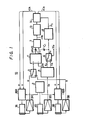
- an automatic control circuit 10 as shown in Fig. 1 is used to automatically adjust the deflection centers thereof.
- reference numerals lR, 1G and 1B respectively designate pick-up tubes or image sensors for red, green and blue colors.
- the deflection center of the green image sensor 1G is taken as a reference, the vertical and horizontal centerings of other red and blue image sensors 1R and 1B are adjusted.
- a deflection signal useful for the horizontal and vertical deflections supplied from a sawtooth wave signal generating circuit 2 to the green image sensor 1G is such one that it is added with the biases corresponding 1H (H represents the horizontal period) in the vertical direction of the picture screen and (T ⁇ H is satisfied) in the horizontal direction so that the green image sensor 1G produces a green signal Go (see Fig. 2A) which is advanced in phase by (1H + ) relative to red and blue signals R and B produced from red and green image sensors lR and 1B.
- the green signal Go is supplied through a preamplifier 3G to a generating circuit 5 which generates a comparing reference signal G'o and edge signals E V and E H .
- the reference signal G'o (see Fig. 2B) is delayed in phase by (1H + ) relative to the green signal Go and approximately in equiphase with the red and blue signals R and B.
- the edge signal E V is the edge signal in the vertical direction and used to adjust the vertical centering.
- This edge signal E V is formed of the green signal Go and a signal which results from delaying the green signal Go by 2H. Accordingly, the edge signal E v is such a signal which has the pulse width and the polarity as shown in Fig. 2C.
- the other edge signal E H is used to adjust the horizontal centering.
- one edge signal E V is first selected by a switching circuit 6 to which the edge signals E v and E H are applied and then supplied through a capacitor C 1 for D C cutting to a multiplier 7.
- the edge signal E V is further supplied to a generating circuit 8 which generates a sampling pulse P s (see Fig. 2G).
- the red and blue signals R and B are respectively supplied through preamplifiers 3R and 3B to a switching circuit 9. Then, the selected one of the primary color signals and the reference signal G'o are both supplied to a voltage comparator 11 which detects error signals ⁇ R and ⁇ B corresponding to positional displacements of the red and blue signals R and B relative to the reference signal G'o.
- Figs. 2D and 2E show examples of the red signal R and its error signal ⁇ R relative to the reference signal G'o. The error signal ⁇ R will be described hereinafter.
- the error signal ⁇ R is supplied through a capacitor C 2 for DC cutting to the multiplier 7 thereby multiplied with the edge signal E V .
- a multiplied output ⁇ M R (see Fig. 2F) is produced thereby in which its pulse width corresponds to the displacement amount of the center position of the picture image and its polarity corresponds to the direction of displacement.
- the mulitplied output ⁇ M R is smoothed by a low-pass filter 13 and sampled and then held by a sample hold circuit 14 to which the sampling pulse P s is applied.
- the held output ⁇ C R (see Fig. 2H) is supplied to a deflection correcting circuit 16R in which a vertical deflection signal applied thereto from the generator 2 is corrected and then supplied to red image sensor lR.
- a held output ⁇ C B corresponding to the error signal ⁇ B is similarly generated and supplied to a deflection correcting circuit 16B by which a vertical deflection signal applied thereto from the generator 2 is corrected and then supplied to the blue image sensor 1B.
- the horizontal centering is adjusted after the vertical centering is adjusted. At that time, the edge signal E H is selected by the switching circuit 6.
- the edge signals E V and E H are formed on the basis of an object existing within a predetermined window area S w including the center of a picture screen S as shown in Fig. 3.
- the sampling pulse P S is formed on the basis of the edge signals E V and E H , so even if an object containing much edge components and an object containing less edge components are same in displacement amount of the deflection center, the number of samplings is different and-so the held outputs AC ( ⁇ C R or ⁇ C B ) are naturally different in value.
- the automatic control circuit 10 as shown in Fig. 1 is used to control the gains of gain control circuits (not shown) provided at the rear stages of the preamplifiers 3R and 3B. Also at that time, since the object existing within the predetermined window area S W of the picture screen S is used and the level of the chrominance signal is sampled and held and the output thereof is used to carry out the balance adjustment. Therefore, under different pick-up or shooting conditions, the correcting signal for adjusting the white balance becomes sometimes different. In consequence, so long as the control system having the circuit arrangement as shown in Figure 1 is used, a similar defect to that in the centering adjustment operation takes place.
- the reason why the level compared output ⁇ G V is selected as a converging reference value is that a correct converging reference value must be obtained at all times regardless of the gain and the temperature drift of the automatic control loop. If an absolute converging reference value is used, there may be such a fear that even if the positional displacement is same, the temperature drift and the like, if any, cause the values AR and AB to be changed and hence the deflection center can not be adjusted completly. If the level compared output ⁇ G V is used, the level compared output ⁇ G V itself is affected in advance by the temperature drift and is therefore free from such fear.
- the reference signal G'o is supplied to one switching circuit 9 in addition to the red and blue signals R and B.
- reference numeral 30 designates a correcting signal generating apparatus for generating correcting signals which are fed to the deflection correcting circuits 16R and 16B.
- the control signals are formed mainly by a microcomputer 31.
- the held output ⁇ C of the sample and hold circuit 14 is A/D-converted by the use of the microcomputer 31.
- the microcomputer 31 is provided at its input stage with a voltage comparator 32 to which the held output ⁇ C is applied and also provided at its output stage, at which the digital held output ⁇ C D corresponding to the held output ⁇ C is obtained, with a D/A (digital-to-analog) converter 33.
- the D/A-converted output therefrom is supplied to the voltage comparator 32 and the register of the microcomputer 31 is controlled such that this D/A-converted output becomes coincident with the held output ⁇ C.
- the system which includes the voltage comparator 32, the register of the microcomputer 31 and the D/A converter 33 serves as an A/D converting system in which the register of the microcomputer 31 is operated in accordance with the program as a comparing register by each bit in a sequentially comparing type A/D converter.
- the sampling pulse P s corresponding to the number of the edge components of the object existing within the window area S w is supplied to a counter 35 in which the number of the edge components in the vertical and horizontal directions is counted.
- This counted number of edge components is supplied to the microcomputer 31 which detects whether the edge components with the number necessary for the centering adjustment exist or not. When the number of edge components thus detected is beyond a predetermined number, the microcomputer 31 produces a new control data (a correcting data) which corresponds to the correcting signal. In other cases, an error signal is generated and a control data used prior to the centering adjustment is produced as the control data.
- the control data D C (for example, data of 8 bits) derived from the microcomputer 31 is converted in the form of an analog signal by a D/A converter 37 and distributed to a corresponding control system by a demultiplexer 38.
- the analog control signal namely, the deflection correcting signal S C is selected to be supplied to a line 2 RV .
- the selection of lines is carried out on the basis of the command data supplied thereto from the microcomputer 31.
- Circuits 40H to 41V and circuits 42H to 43V respectively connected to lines l RV' l RH , l BV and l BH are hold circuits and output amplifiers, respectively.
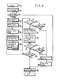
- Fig. 6 is a flow chart useful for explaining the centering adjusting modes.
- the centering adjusting mode begins with the step 49.
- the step 50 the number of edge components in the horizontal and vertical directions of the object existing within the window area S W is checked.
- the control data D C prior to the centering adjustment is moved to a save area in the step 52.
- a loop counter is reset to "1" and at the following step 54, an error flag is reset.
- the vertical reference signal ⁇ G V is detected. This standby time is used to carry out data processing after the transient period is passed.
- the vertical reference signal ⁇ G V is stored in the memory.
- This subroutine 60 is used to carry out the adjustment of the vertical centering for the red and blue image sensors lR and 1B.
- step 71 whether the vertical centering adjustemnt lies within a predetermined converging value or not is detected. Unless the converging value is error, the processing step is advanced to the step 72 wherein after the standby time of (6V + t), the detection of the horizontal reference signal ⁇ G H is executed for the adjustment of the horizontal centering.
- the processing step is moved to a second subroutine shown by the step 73 in which the adjustment of the horizontal centering for the red and blue image sensors lR and 1B is executed similary as before.
- the horizontal centering After the horizontal centering is adjusted, whether the horizontal deflection correcting signal lies within a predetermined converging value or not is judged at the step 74. When no error exists, whether the adjusting mode is the second adjusting mode or not is judged at the step 75. If the adjusting mode is the first adjusting mode, the processing step is returned to the step 54 and then the similar operation is repeated. When the second adjusting mode is ended, the result of the centering adjustment (satisfactory or erroneous) is indicated at the step 76.
- the number of the automatic adjustements is not limited to twice.
- the first and second subroutines are different only in that the object to be controlled is either the vertical deflection system or the horizontal deflection system. Therefore, only the first subroutine will be described.
- Fig. 7 is a flow chart of an example of a subroutine CSR used for adjusting the vertical centering.
- a control data data of a second channel CH-2 regarding the blue image sensor lB is moved to the save area and the control (control of a first channel CH-1) regarding the red image sensor lR is executed first.
- a line selecting signal which selects the lines l RV and l RH corresponding to the channel number CH-NO is supplied to the demultiplexer 38.
- the initial value of a reference correcting data D F is selected to be, for example, 1/16 of the maximum correcting amount (00010000 in the case of the data formed of 8 bits).
- the reference correcting data D F is subtracted from the control data D C , while when the error data a is negative, the reference correcting data D F is added to the control data D C .
- a new control data D C in which the reference correcting data D F is added to the control data D C is used as the correcting signal for the vertical centering adjustment.
- the vertical centering is not converged immediately to the predetermined value by the correcting signal. That is, the result corrected by the new control data D C is calculated again at the step 63 and the same reference correcting data D F as before is again added to the control data D C so as to produce a new control data D C .
- the error data A is gradually decreased and hence the correction becomes overcorrection at last, thus, the polarity of the error data ⁇ is inverted (see Fig. 9).
- the inversion of the polarity is judged by the step 64 and whether the reference correcting data D F is 1 LSB (least significant bit) or hot is judged at the next step 66.
- the reference correcting data D F is changed to 1/2 at the step 67.
- the reference correcting data D F is decreased to 1/2, 1/4, 1/8 ... each time the polarity of the error data ⁇ is inverted. Accordingly, when the number of the inversions is taken as n, becomes the reference correcting data D F at that time.
- step 90 If such control is sequentially repeated, the error data ⁇ is gradually decreased and the reference correcting data D F becomes 1 LSB finally, which then is detected at the step 66. Then, the control mode is moved to a third subroutine (step 90).
- the fine adjustment of the vertical centering is carried out and each time the polarity of the error data A is inverted, the control data D C is stored.
- the control mode M is stopped and an average value D Ci /M of the accumulated value of the stored control data D C is used as the final control data D C .
- the loop counter used for inverting the polarity is set to "1".
- the cycle counter for overflow is reset to "0", and at the next step 93, the standby of 1 vertical period (1 V period) is carried out.
- the error data A is calculated and the polarity inversion of the error data ⁇ is detected at the step 95. If the polarity of the error data ⁇ is not changed, the mode is moved to the step 96 in which the positive and negative polarity of the error data ⁇ are judged.
- the reference correcting data D F of 1 LSB is subtracted from the control data D C at the step 97 to produce a new control data D C and thereafter, the cycle counter is incremented by "1" at the step 98.
- the reference correcting data D F of 1 LSB is added to the control data D C at the step 99 to produce a new control data D C and the cycle counter is similarly incremented by "1" at the step 98.
- the mode is again returend to the step 93. Thereafter, the centering adjustment is carried out on the basis of the new control data D C which results from adding to or subtracting from the control data D C the reference correcting data D F of 1 LSB.
- the polarity of the error data ⁇ is inverted so that when the polarity of the error data ⁇ is inverted, the control data D C at that time is stored in the calculation area at the step 102.
- the loop counter is incremented by "1" at the step 103 and until the number of the increments of the loop counter reaches M times, the similar operation is repeated.
- the average value ( ) of the accumulated control data stored in the calculation area is calculated (at the step 105).
- the averaged control data is supplied to the corresponding correcting circuits 16R and 16B as the final control data D C , respectively.
- the error data ⁇ itself is not used for adjusting the vertical and horizontal centering. But instead, as shown in Fig. 9, the signal formed by adding the reference correcting data (initial value) D F calculated from the detected error data ⁇ to the correcting signal (the control data D C ) is used as the correcting signal for adjusting the centering and then, until the polarity of the new error data ⁇ resulting from the addition of this correcting signal is inverted, the above reference correcting data D F is added to the control signal D C to thereby sequentially correct the same.
- the reference correcting data D F initial value
- the overcorrection and insufficient correction are alternately carried out so as to obtain the final control data so that regardless of the number of edge components in the horizontal and vertical directions, accordingly, whether the relation between the displacement of the centering and the control data D C is presented as shown by the straight line a or b in the graph of Fig. 4 the similar correction can be carried out.
- the control signal D C it is possible to converge the control signal D C to the correct converging value surely.
- Fig- 10 is a conceptual diagram showing the above converging method of the invention.
- the reference correcting data D F obtained on the basis of the data ⁇ C (accordingly, ⁇ ) produced from a data detecting means 110 and derived from a reference correcting data generating means 111 is mixed to the control data D C in a mixing means 112 to become the new control data D C .
- the polarity of the reference correcting data D F is controlled by the output from the polarity judging means 113 and a change command means.115 is operated by the output from a polarity inversion detecting means 114 whereby the value of the reference correcting data D F is changed in accordance with the number of polarity inversions.
- a control end signal generating means 119 generates the correcting signal by which the converging loop is stopped.
- the present invention is applied to the vertical and horizontal centering control system, it is neeedless to say that this invention can also be applied to the white balance control system.
- the object to be corrected in the controlled system can surely be converged to the predetermined value so that the automatic control accuracy can be increased largely.
Landscapes
- Engineering & Computer Science (AREA)
- Multimedia (AREA)
- Signal Processing (AREA)
- Color Television Image Signal Generators (AREA)
- Details Of Television Scanning (AREA)
Applications Claiming Priority (2)
| Application Number | Priority Date | Filing Date | Title |
|---|---|---|---|
| JP58175427A JPS6068779A (ja) | 1983-09-22 | 1983-09-22 | ビデオカメラの自動制御回路 |
| JP175427/83 | 1983-09-22 |
Publications (2)
| Publication Number | Publication Date |
|---|---|
| EP0136164A1 true EP0136164A1 (fr) | 1985-04-03 |
| EP0136164B1 EP0136164B1 (fr) | 1988-02-17 |
Family
ID=15995907
Family Applications (1)
| Application Number | Title | Priority Date | Filing Date |
|---|---|---|---|
| EP84306486A Expired EP0136164B1 (fr) | 1983-09-22 | 1984-09-21 | Circuit de réglage automatique de gain |
Country Status (5)
| Country | Link |
|---|---|
| US (1) | US4622581A (fr) |
| EP (1) | EP0136164B1 (fr) |
| JP (1) | JPS6068779A (fr) |
| CA (1) | CA1207892A (fr) |
| DE (1) | DE3469397D1 (fr) |
Cited By (1)
| Publication number | Priority date | Publication date | Assignee | Title |
|---|---|---|---|---|
| EP0159184A1 (fr) * | 1984-04-16 | 1985-10-23 | Sony Corporation | Appareil et procédé pour centrage automatique d'une caméra vidéo |
Families Citing this family (2)
| Publication number | Priority date | Publication date | Assignee | Title |
|---|---|---|---|---|
| GB2203919B (en) * | 1987-04-22 | 1991-02-20 | Sony Corp | Registration adjustment in colour television cameras |
| JP2615065B2 (ja) * | 1987-08-28 | 1997-05-28 | 富士写真フイルム株式会社 | カメラの白バランス調整方法 |
Citations (2)
| Publication number | Priority date | Publication date | Assignee | Title |
|---|---|---|---|---|
| DE2224143A1 (de) * | 1971-05-17 | 1972-11-30 | Rca Corp | Regelungseinrichtung zur automatischen Farbdeckung bei Farbfernsehkameras |
| US4314272A (en) * | 1979-04-09 | 1982-02-02 | Tokyo Shibaura Denki Kabushiki Kaisha | Adjusting device for color television camera apparatus |
Family Cites Families (5)
| Publication number | Priority date | Publication date | Assignee | Title |
|---|---|---|---|---|
| JPS5650685A (en) * | 1979-09-29 | 1981-05-07 | Sony Corp | Multi-tube type image pickup device |
| JPS604637B2 (ja) * | 1980-06-02 | 1985-02-05 | 日本ビクター株式会社 | テレビジヨンカメラにおける自動白色調節回路 |
| US4335397A (en) * | 1980-06-24 | 1982-06-15 | Sony Corporation | Method and apparatus for digitally adjusting white balance |
| JPS587991A (ja) * | 1981-07-08 | 1983-01-17 | Sony Corp | 多管式カラ−カメラのレジストレ−シヨン調整回路 |
| JPS589495A (ja) * | 1981-07-08 | 1983-01-19 | Sony Corp | 多管式カラ−カメラのレジストレ−シヨン調整回路 |
-
1983
- 1983-09-22 JP JP58175427A patent/JPS6068779A/ja active Pending
-
1984
- 1984-09-19 CA CA000463532A patent/CA1207892A/fr not_active Expired
- 1984-09-19 US US06/652,084 patent/US4622581A/en not_active Expired - Lifetime
- 1984-09-21 DE DE8484306486T patent/DE3469397D1/de not_active Expired
- 1984-09-21 EP EP84306486A patent/EP0136164B1/fr not_active Expired
Patent Citations (2)
| Publication number | Priority date | Publication date | Assignee | Title |
|---|---|---|---|---|
| DE2224143A1 (de) * | 1971-05-17 | 1972-11-30 | Rca Corp | Regelungseinrichtung zur automatischen Farbdeckung bei Farbfernsehkameras |
| US4314272A (en) * | 1979-04-09 | 1982-02-02 | Tokyo Shibaura Denki Kabushiki Kaisha | Adjusting device for color television camera apparatus |
Cited By (1)
| Publication number | Priority date | Publication date | Assignee | Title |
|---|---|---|---|---|
| EP0159184A1 (fr) * | 1984-04-16 | 1985-10-23 | Sony Corporation | Appareil et procédé pour centrage automatique d'une caméra vidéo |
Also Published As
| Publication number | Publication date |
|---|---|
| DE3469397D1 (en) | 1988-03-24 |
| US4622581A (en) | 1986-11-11 |
| JPS6068779A (ja) | 1985-04-19 |
| CA1207892A (fr) | 1986-07-15 |
| EP0136164B1 (fr) | 1988-02-17 |
Similar Documents
| Publication | Publication Date | Title |
|---|---|---|
| US5659355A (en) | CCD dark mean level correction circuit employing digital processing and analog subtraction requiring no advance knowledge of dark mean level | |
| US5341218A (en) | Video signals clamping circuit for maintaining DC level of video signals | |
| EP0240937B1 (fr) | Circuit pour la correction du niveau du noir pour caméras vidéo | |
| US20080170086A1 (en) | Front end signal processing method and front end signal processor | |
| US4335397A (en) | Method and apparatus for digitally adjusting white balance | |
| US6195133B1 (en) | Digital automatic gain control (AGC) circuit | |
| EP0136164B1 (fr) | Circuit de réglage automatique de gain | |
| US4731652A (en) | Shading correction signal generating device for a television camera apparatus | |
| GB2052209A (en) | White balance control for colour video cameras | |
| JP2568425B2 (ja) | コンポーネント・テレビジョン用タイミング補正器 | |
| JPH07193755A (ja) | デジタルクランプ回路 | |
| US4823188A (en) | Apparatus for correcting for shading defects in video signals induced by variations in the speed of scanning spots in a TV camera | |
| JP2618909B2 (ja) | 自動白バランス調整方法及び装置 | |
| JP2826966B2 (ja) | ベクトル基準目盛り自動生成装置 | |
| US7391474B2 (en) | Display interface systems and methods | |
| JPH0634509B2 (ja) | ホワイトバランス補正回路 | |
| JPH0695764B2 (ja) | 撮像装置 | |
| JPH05153428A (ja) | クランプ回路 | |
| KR19980051981A (ko) | 투사형 티브이(tv)에서의 컨버젼스 보정장치와 그 제어방법 | |
| JPH0552708B2 (fr) | ||
| JPH0321106Y2 (fr) | ||
| JPH08265667A (ja) | デジタル・アナログ変換装置 | |
| JP3286989B2 (ja) | 可変利得制御回路とビデオカメラ | |
| JPH05328367A (ja) | カラーテレビジョンカメラ装置 | |
| JPH0546752B2 (fr) |
Legal Events
| Date | Code | Title | Description |
|---|---|---|---|
| PUAI | Public reference made under article 153(3) epc to a published international application that has entered the european phase |
Free format text: ORIGINAL CODE: 0009012 |
|
| 17P | Request for examination filed |
Effective date: 19841002 |
|
| AK | Designated contracting states |
Designated state(s): DE FR GB NL |
|
| 17Q | First examination report despatched |
Effective date: 19860714 |
|
| GRAA | (expected) grant |
Free format text: ORIGINAL CODE: 0009210 |
|
| AK | Designated contracting states |
Kind code of ref document: B1 Designated state(s): DE FR GB NL |
|
| REF | Corresponds to: |
Ref document number: 3469397 Country of ref document: DE Date of ref document: 19880324 |
|
| ET | Fr: translation filed | ||
| PLBE | No opposition filed within time limit |
Free format text: ORIGINAL CODE: 0009261 |
|
| STAA | Information on the status of an ep patent application or granted ep patent |
Free format text: STATUS: NO OPPOSITION FILED WITHIN TIME LIMIT |
|
| 26N | No opposition filed | ||
| PGFP | Annual fee paid to national office [announced via postgrant information from national office to epo] |
Ref country code: FR Payment date: 20010911 Year of fee payment: 18 |
|
| PGFP | Annual fee paid to national office [announced via postgrant information from national office to epo] |
Ref country code: GB Payment date: 20010919 Year of fee payment: 18 |
|
| PGFP | Annual fee paid to national office [announced via postgrant information from national office to epo] |
Ref country code: NL Payment date: 20010927 Year of fee payment: 18 |
|
| PGFP | Annual fee paid to national office [announced via postgrant information from national office to epo] |
Ref country code: DE Payment date: 20011009 Year of fee payment: 18 |
|
| REG | Reference to a national code |
Ref country code: GB Ref legal event code: IF02 |
|
| PG25 | Lapsed in a contracting state [announced via postgrant information from national office to epo] |
Ref country code: GB Free format text: LAPSE BECAUSE OF NON-PAYMENT OF DUE FEES Effective date: 20020921 |
|
| PG25 | Lapsed in a contracting state [announced via postgrant information from national office to epo] |
Ref country code: NL Free format text: LAPSE BECAUSE OF NON-PAYMENT OF DUE FEES Effective date: 20030401 Ref country code: DE Free format text: LAPSE BECAUSE OF NON-PAYMENT OF DUE FEES Effective date: 20030401 |
|
| GBPC | Gb: european patent ceased through non-payment of renewal fee |
Effective date: 20020921 |
|
| PG25 | Lapsed in a contracting state [announced via postgrant information from national office to epo] |
Ref country code: FR Free format text: LAPSE BECAUSE OF NON-PAYMENT OF DUE FEES Effective date: 20030603 |
|
| REG | Reference to a national code |
Ref country code: FR Ref legal event code: ST |