EP0136880A1 - Integrierte Halbleiterschaltung vom 'Gate-Array'-Typ - Google Patents
Integrierte Halbleiterschaltung vom 'Gate-Array'-Typ Download PDFInfo
- Publication number
- EP0136880A1 EP0136880A1 EP84306557A EP84306557A EP0136880A1 EP 0136880 A1 EP0136880 A1 EP 0136880A1 EP 84306557 A EP84306557 A EP 84306557A EP 84306557 A EP84306557 A EP 84306557A EP 0136880 A1 EP0136880 A1 EP 0136880A1
- Authority
- EP
- European Patent Office
- Prior art keywords
- diffusion regions
- basic cells
- gate array
- spaces
- basic
- Prior art date
- Legal status (The legal status is an assumption and is not a legal conclusion. Google has not performed a legal analysis and makes no representation as to the accuracy of the status listed.)
- Granted
Links
Images



Classifications
-
- H—ELECTRICITY
- H10—SEMICONDUCTOR DEVICES; ELECTRIC SOLID-STATE DEVICES NOT OTHERWISE PROVIDED FOR
- H10D—INORGANIC ELECTRIC SEMICONDUCTOR DEVICES
- H10D84/00—Integrated devices formed in or on semiconductor substrates that comprise only semiconducting layers, e.g. on Si wafers or on GaAs-on-Si wafers
- H10D84/80—Integrated devices formed in or on semiconductor substrates that comprise only semiconducting layers, e.g. on Si wafers or on GaAs-on-Si wafers characterised by the integration of at least one component covered by groups H10D12/00 or H10D30/00, e.g. integration of IGFETs
- H10D84/82—Integrated devices formed in or on semiconductor substrates that comprise only semiconducting layers, e.g. on Si wafers or on GaAs-on-Si wafers characterised by the integration of at least one component covered by groups H10D12/00 or H10D30/00, e.g. integration of IGFETs of only field-effect components
- H10D84/83—Integrated devices formed in or on semiconductor substrates that comprise only semiconducting layers, e.g. on Si wafers or on GaAs-on-Si wafers characterised by the integration of at least one component covered by groups H10D12/00 or H10D30/00, e.g. integration of IGFETs of only field-effect components of only insulated-gate FETs [IGFET]
- H10D84/85—Complementary IGFETs, e.g. CMOS
- H10D84/854—Complementary IGFETs, e.g. CMOS comprising arrangements for preventing bipolar actions between the different IGFET regions, e.g. arrangements for latchup prevention
-
- H—ELECTRICITY
- H10—SEMICONDUCTOR DEVICES; ELECTRIC SOLID-STATE DEVICES NOT OTHERWISE PROVIDED FOR
- H10D—INORGANIC ELECTRIC SEMICONDUCTOR DEVICES
- H10D84/00—Integrated devices formed in or on semiconductor substrates that comprise only semiconducting layers, e.g. on Si wafers or on GaAs-on-Si wafers
- H10D84/01—Manufacture or treatment
-
- H—ELECTRICITY
- H10—SEMICONDUCTOR DEVICES; ELECTRIC SOLID-STATE DEVICES NOT OTHERWISE PROVIDED FOR
- H10D—INORGANIC ELECTRIC SEMICONDUCTOR DEVICES
- H10D84/00—Integrated devices formed in or on semiconductor substrates that comprise only semiconducting layers, e.g. on Si wafers or on GaAs-on-Si wafers
- H10D84/01—Manufacture or treatment
- H10D84/02—Manufacture or treatment characterised by using material-based technologies
- H10D84/03—Manufacture or treatment characterised by using material-based technologies using Group IV technology, e.g. silicon technology or silicon-carbide [SiC] technology
- H10D84/038—Manufacture or treatment characterised by using material-based technologies using Group IV technology, e.g. silicon technology or silicon-carbide [SiC] technology using silicon technology, e.g. SiGe
-
- H—ELECTRICITY
- H10—SEMICONDUCTOR DEVICES; ELECTRIC SOLID-STATE DEVICES NOT OTHERWISE PROVIDED FOR
- H10D—INORGANIC ELECTRIC SEMICONDUCTOR DEVICES
- H10D84/00—Integrated devices formed in or on semiconductor substrates that comprise only semiconducting layers, e.g. on Si wafers or on GaAs-on-Si wafers
- H10D84/90—Masterslice integrated circuits
- H10D84/903—Masterslice integrated circuits comprising field effect technology
- H10D84/907—CMOS gate arrays
Definitions
- the present invention relates to a semiconductor integrated circuit (IC) device, more particularly, to a semiconductor IC device of the gate array type fabricated with complementary metal insulator semiconductor (CMIS) transistors.
- IC semiconductor integrated circuit
- CMIS complementary metal insulator semiconductor
- a masterslice semiconductor device As is well known, many basic element sets are formed in advance in a semiconductor chip. Each basic element set is fabricated with usual transistors, resistors, and so on to form a basic circuit (hereinafter referred to as a basic cell). The masterslice semiconductor device is mass produced. Interconnecting lines are then formed between the basic cells and in each basic cell using a specified mask to obtain an LSI semiconductor device with the desired functional circuits.
- This technique enables significant reductions in both design and manufcaturing time since one need only design and fabricate the masks when manufacturing a new LSI semiconductor device. Furthermore, in a masterslice semiconductor device, since a large number of basic cells are regularly arranged in both the column and row directions on the semiconductor substrate and form a standardized matrix pattern, it is very easy to employ so-called computer aided automatic wiring for forming the interconnecting wiring lines.
- Such a standardized matrix pattern is usually called a "gate array".
- a CMIS gate array is most widely used for LSI semiconductor devices.
- the basic cells of such an array each comprise CMIS transistors.
- CMIS transistor have the advantage of low-power operation and, therefore, provide higher integration of the LSI semiconductor device.
- CMIS gate array type LSI semiconductor devices suffer from the problem of "latchup".
- latchup In the latchup phenomenon, a parasitic silicon-controlled rectifier (SCR) is created in the substrate. This SCR, when remaining on, can break the interconnecting lines and damage the basic cells.
- SCR parasitic silicon-controlled rectifier
- a gate array type of semiconductor integrated circuit device formed in a semiconductor substrate, comprising an array of basic cells arranged in columns and rows with column spaces between adjacent columns and row spaces between adjacent rows, each of the basic cells including a first-channel MIS transistor formed in the silicon substrate of one conductivity type and a second-channel MIS transistor formed in a well of other conductivity type; a plurality of first diffusion regions of one conductivity type in contact with the semiconductor substrate and located in the row spaces between adjacent basic cells, the first diffusion regions being ohmically connected with a first power line, and a plurality of second diffusion regions of the other conductivity type in contact with the wells and located in the row spaces between adjacent basic cells, the second diffusion regions being ohmically connected with a second power line.
- the insertion of the n + - and p +- diffusion regions between each two adjacent basic cells impedes higher densities of packing of the basic cells and thus reduces the integration degree of the device.
- both the first and second diffusion regions have a comb-shaped structure arranged with itsbase along the column spaces and its teeth along the row spaces.
- Figure 1 is a circuit diagram of a conventional basic cell used in a CMIS gate array type LSI smiconductor device.
- the basic cell of Figure 1 known from US-A-4,412,237 comprises two p-channel MIS transistors TR 1 , TR 2 and two n-channel MIS transistors TR3 , TR4. Each two MIS transistors of the same channel have a common source or drain. In addition, each two MIS transistors of different channels have common gates.
- Figure 2 is an enlarged top plan view of the basic cell shown in Figure 1 formed on a semiconductor substrate. Specifically, the pattern of the regions with impurities and the pattern of the gate electrodes for realizing the basic cell are illustrated in Figure 2.
- Reference numeral 1 represents a first gate electrode wiring layer, made of, for example, polycrystalline silicon, and 2 a second gate electrode wiring layer, also made polycrystalline silicon.
- Reference numerals 3, 4 and 5 represent n +- type regions for forming the source or drain of the n-channel transistors.
- Reference numerals 6, 7, and 8 represent p +-type regions for forming the source or drain of the p-channel transistors.
- Reference numeral 9 represents an island-like p-type region, i.e., a so-called p-type well, and 10 an n-type silicon substrate.
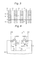
- Figure 3 is a top plan view of a basic cell arrangement on a semiconductor chip.
- reference numeral 11 represents basic cells as explained in detail before. Spaces 12 are formed between these basic cells 11 for arranging interconnecting lines in the row direction. At the same time, spaces 13 are formed for arranging interconnecting lines in the column direction.
- each of the basic cell arrays includes tens to hundreds of basic cells in the column diretion. Tens of the basic cell arrays are arranged in the row direction. The width of each row space 12 is determined so that one to four interconnecting lines can be accommodated therein, while the width of each column space 13 is determined so that ten to several tens of interconnecting lines can be accomodated therein.
- FIG. 4 is a cross-sectional view and equivalent circuit diagram for explaining the latchup phenomenon.
- a parasitic npn transistor T 1 is formed in the p-type well at the nMIS side and a parasitic pnp transistor T 2 is formed in the n-type silicon substrate 10 at the pMIS side.
- parasitic resistors R 1 , R 2 , R 3 , and R 4 are defined between each emitter, base and collector of the parasitic transistors T 1 and T 2 .
- the parasitic transistors and the parasitic resistors provide a thyristor structure. Latchup is caused by the thus formed thyristor.
- the resistance values of the parasitic resistors R 1 , R 2 , R 3 , and R 4 can be reduced by lowering the resistance values of the n-type silicon substrate 10 itself and the p-type well 9 itself.
- an n -diffusion region and a p + -diffusion region are formed respectively in the surface layers of the n-type silicon substrate 10 and p-type well 9, for contact therewith in the vicinity of each transistor pMIS and each transistor nMIS.
- each diffusion region must make contact with the power lines of V DD and V SS . This increases the width of each diffusion region and, therefore, necessitates that the basic cells in each basic cell array be separated in the column direction with a wide pitch. This impedes higher density of packing.
- Figure 5 is an enlarged top plan view of the partial basic cell array shown in Figure 3.
- members the same as those of previous figures are represented by the same reference numerals or symbols (same for later figures).
- the prior art n +- diffusion regions 15 for contacting the n-type silicon substrate 10 are formed independently between each two adjacent basic cells 11.
- the prior art p +- diffusion regions 14 for contacting the p-type well 9 are formed independently between each two adjacent basic cells 11.
- the symbol "X" denotes an ohmic contact for connection to the power line of V DD or V SS .
- the existence of the ohmic contact at each diffusion region (14, 15) increases the width of the regions and, in this sense impedes higher density of packing of the basic cells.
- Figure 6A and Figure 6B schematically show basic structures of a first type diffusion region and second type diffusion region according to the present invention.
- the diffusion regions of the present invention for contact with the n-type silicon substrate and the p-type well are comb-shaped in overall structure.
- the first type comb-shaped diffusion region is shaped with a base part a, wide tooth parts b, and narrow tooth parts c. Each wide tooth part 6 contains an ohmic contact X for contact with the power line.
- the second type comb-shaped diffusion region is shaped with the base part a and the narrow tooth parts c.
- the base part a contains the ohmic contacts X.
- Figure 7A is an enlarged top plan view of a partial basic cell array according to a first embodiment of the present invention.
- Figure 7D is an enlarged cross-sectional view taken along line D-D of Figure 7A.
- Members 1 through 13 in Figures 7A through 7D, have already been explained.
- Reference numerals lA, 1B, and 1C represent three different terminal electrodes provided by the first gate electrode wiring layer 1.
- 2A, 2B, and 2C represent three different terminal electrodes provided by the second gate electrode wiring layer 2.
- Reference numeral 16 represents an isolation layer for separation and 17 a gate insulation layer.
- Reference numeral 18 represents an n +- diffusion region for contact with the n-type silicon substrate 10, and reference numeral 19 represents a p -diffusion region for contact with the p-type well 9.
- reference numeral 18a represents a base part of the region 18, 18b wide tooth parts of the region 18, and 18c narrow tooth parts of the region 18.
- the base part 18a has a belt-like shape and is on the order of several ⁇ m width for a relatively low resistance value.
- Each of the wide tooth parts 18b is on the order of several ⁇ m width for contact with the power line of V DD through an individual ohmic contact (X) window 20, usually formed in an insulation layer made of, for example, phospho-silicate glass (PSG) mounted on the basic cells.
- X individual ohmic contact
- Each of the narrow tooth parts 18c is as narrow as possible, i.e., the minimum width possible with recent semiconductor manufacturing techniques.
- reference numeral 19a represents a base part of the region 19, 19b wide tooth parts of the region 19, and 19c narrow tooth parts of the region 19.
- the base part 19a has a belt-like shape and is on the order of several ⁇ m width for a relatively low resistance value.
- Each of the wide tooth parts 19b is on the order of several um width in order for contact with the power line of V SS through an individual ohmic contact (X) window 21 identical to the window 20.
- Each of the narrow tooth parts 19c is as narrow as possible, i.e., the minimum width possible with recent semiconductor manufacturing techniques.
- Each part of the n + - and p -diffusion regions is 0 formed to be about several thousand A in depth, almost the same as that of each source and drain of the CMIS transistors comprising each basic cell.
- the wide tooth parts 18b and 19b are located in the column direction with at a pitch corresponding to two successive basic cells 11.
- the wide tooth parts 18b and 19b may also be located at a pitch corresponding to three or more successive basic cells so long as the capability of suppressing latchup is maintained.
- the basic cells can be packed at a high degree of density while maintaining a capability for suppressing latchup comparable with the prior art for each basic cell sandwiched by two tooth parts (18b, 18c; 19b, 19c) located close thereto.
- the base, wide tooth, and narrow tooth parts (18a, 18b, 18c) of the n + -type can be manufactured at the same time as the source and drain of the n-channel MIS transistors nMIS.
- the base, wide tooth, and narrow tooth parts (19a, 19b, 19c) of the p + -type can be manufactured at the same time as the source and drain of the p-channel MIS transistors pMIS.
- Figure 8 is an enlarged top plan view of a partial basic cell array according to a second embodiment of the present invention. This figure corresponds to Figure 7A of the first embodiment. The major part is substantially the same as Figure 7A. The differences here are that the tooth parts are all formed with the narrow tooth parts 18c and 19c, that is, the wide tooth parts 18b and 19b are removed therefrom. Therefore, the ohmic contact (X) windows 22 and 23 are formed right above the base parts 18a and 19a respectively.
- FIG 9 is a schematic top plan view of an example of a gate array type semiconductor integrated circuit device including the comb-shaped diffusion regions acccording to the first embodiment of Figure 7A.
- the length of each basic call array in the column direction may be 9.6 mm.
- the prior art diffusion regions shown in Figure 5 are utilized, 300 basic cells can be accommodated in each basic cell array. Since the pitch P 1 (refer to Figure 5) between two successive diffusion regions is usually about 32 ⁇ m and the width W 1 (refer to Figure 5) of each diffusion region is about 4 ⁇ m, the expression 300 x 32 ( ⁇ m) - 9.6 (mm) stands.
- the width W 1 (refer to Figure 7A) of each wide tooth part is about 4 ⁇ m as in the prior art
- the width W 2 (refer to Figure 7A) of each narrow tooth part can be halved to about 2 ⁇ m. Therefore, the pitch P 2 (refer to Figure 7A) between two successive diffusion regions can be reduced to 30 ⁇ m.
- the pitch P 2 becomes shorter by 2 ⁇ m than the pitch P 1 of the prior art.
- a comb-shaped diffusion region comprised of at least narrow tooth parts can save chip space for further basic cells.
- the thus saved chip space necessarily becomes large, which is sufficient to accommodate many further basic cells in each basic cell array.
Landscapes
- Design And Manufacture Of Integrated Circuits (AREA)
- Metal-Oxide And Bipolar Metal-Oxide Semiconductor Integrated Circuits (AREA)
Applications Claiming Priority (2)
| Application Number | Priority Date | Filing Date | Title |
|---|---|---|---|
| JP182069/83 | 1983-09-30 | ||
| JP58182069A JPH0828480B2 (ja) | 1983-09-30 | 1983-09-30 | 半導体集積回路装置 |
Publications (2)
| Publication Number | Publication Date |
|---|---|
| EP0136880A1 true EP0136880A1 (de) | 1985-04-10 |
| EP0136880B1 EP0136880B1 (de) | 1987-12-16 |
Family
ID=16111804
Family Applications (1)
| Application Number | Title | Priority Date | Filing Date |
|---|---|---|---|
| EP84306557A Expired EP0136880B1 (de) | 1983-09-30 | 1984-09-26 | Integrierte Halbleiterschaltung vom 'Gate-Array'-Typ |
Country Status (5)
| Country | Link |
|---|---|
| US (1) | US4701777A (de) |
| EP (1) | EP0136880B1 (de) |
| JP (1) | JPH0828480B2 (de) |
| KR (1) | KR890003299B1 (de) |
| DE (1) | DE3468151D1 (de) |
Cited By (3)
| Publication number | Priority date | Publication date | Assignee | Title |
|---|---|---|---|---|
| DE3714598A1 (de) * | 1986-05-23 | 1987-11-26 | Mitsubishi Electric Corp | Integrierte halbleiterschaltung |
| EP0282082A3 (en) * | 1987-03-13 | 1990-07-18 | Fujitsu Limited | Basic cell of gate array device |
| US6410675B2 (en) | 1998-10-13 | 2002-06-25 | Affymetrix, Inc. | Functionalized silicon compounds and methods for their synthesis and use |
Families Citing this family (17)
| Publication number | Priority date | Publication date | Assignee | Title |
|---|---|---|---|---|
| JPS62119936A (ja) * | 1985-11-19 | 1987-06-01 | Fujitsu Ltd | コンプリメンタリ−lsiチツプ |
| US4884118A (en) * | 1986-05-19 | 1989-11-28 | Lsi Logic Corporation | Double metal HCMOS compacted array |
| US4791317A (en) * | 1986-09-26 | 1988-12-13 | Siemens Aktiengesellschaft | Latch-up protection circuit for integrated circuits using complementary mos circuit technology |
| US4791316A (en) * | 1986-09-26 | 1988-12-13 | Siemens Aktiengesellschaft | Latch-up protection circuit for integrated circuits using complementary MOS circuit technology |
| US5136355A (en) * | 1987-11-25 | 1992-08-04 | Marconi Electronic Devices Limited | Interconnecting layer on a semiconductor substrate |
| US5025296A (en) * | 1988-02-29 | 1991-06-18 | Motorola, Inc. | Center tapped FET |
| EP0338817B1 (de) * | 1988-04-22 | 1999-09-08 | Fujitsu Limited | Integrierte Halbleiterschaltungsanordnung vom "Masterslice"-Typ |
| NL194182C (nl) * | 1988-07-23 | 2001-08-03 | Samsung Electronics Co Ltd | Randloze moederschijf-halfgeleiderinrichting. |
| SG67297A1 (en) * | 1989-04-19 | 1999-09-21 | Seiko Epson Corp | Semiconductor device |
| US5459340A (en) * | 1989-10-03 | 1995-10-17 | Trw Inc. | Adaptive configurable gate array |
| US5217916A (en) * | 1989-10-03 | 1993-06-08 | Trw Inc. | Method of making an adaptive configurable gate array |
| US5200917A (en) * | 1991-11-27 | 1993-04-06 | Micron Technology, Inc. | Stacked printed circuit board device |
| JP4517413B2 (ja) * | 1999-01-13 | 2010-08-04 | ソニー株式会社 | 半導体装置 |
| JP4794030B2 (ja) * | 2000-07-10 | 2011-10-12 | ルネサスエレクトロニクス株式会社 | 半導体装置 |
| US7102867B2 (en) | 2003-06-30 | 2006-09-05 | International Business Machines Corporation | Method, apparatus and circuit for latchup suppression in a gate-array ASIC environment |
| JP5331195B2 (ja) * | 2009-10-19 | 2013-10-30 | パナソニック株式会社 | 半導体装置 |
| KR20180068229A (ko) * | 2016-12-13 | 2018-06-21 | 삼성전자주식회사 | 반도체 장치 및 이의 제조 방법 |
Citations (3)
| Publication number | Priority date | Publication date | Assignee | Title |
|---|---|---|---|---|
| GB1502130A (en) * | 1974-12-30 | 1978-02-22 | Ibm | Integrated circuits |
| EP0009782A1 (de) * | 1978-09-28 | 1980-04-16 | Kabushiki Kaisha Toshiba | CMOS-Halbleitervorrichtung |
| EP0105985A1 (de) * | 1982-10-12 | 1984-04-25 | Mitsubishi Denki Kabushiki Kaisha | Integrierter Schaltkreis mit komplementärem Isolierschicht-Feldeffekt-Halbleiterelement |
Family Cites Families (3)
| Publication number | Priority date | Publication date | Assignee | Title |
|---|---|---|---|---|
| JPS5925381B2 (ja) * | 1977-12-30 | 1984-06-16 | 富士通株式会社 | 半導体集積回路装置 |
| JPS58210660A (ja) * | 1982-06-01 | 1983-12-07 | Seiko Epson Corp | 半導体装置 |
| JPS6017932A (ja) * | 1983-07-09 | 1985-01-29 | Fujitsu Ltd | ゲ−ト・アレイ |
-
1983
- 1983-09-30 JP JP58182069A patent/JPH0828480B2/ja not_active Expired - Lifetime
-
1984
- 1984-09-26 EP EP84306557A patent/EP0136880B1/de not_active Expired
- 1984-09-26 DE DE8484306557T patent/DE3468151D1/de not_active Expired
- 1984-09-28 KR KR8405989A patent/KR890003299B1/ko not_active Expired
-
1986
- 1986-12-30 US US06/948,406 patent/US4701777A/en not_active Expired - Lifetime
Patent Citations (3)
| Publication number | Priority date | Publication date | Assignee | Title |
|---|---|---|---|---|
| GB1502130A (en) * | 1974-12-30 | 1978-02-22 | Ibm | Integrated circuits |
| EP0009782A1 (de) * | 1978-09-28 | 1980-04-16 | Kabushiki Kaisha Toshiba | CMOS-Halbleitervorrichtung |
| EP0105985A1 (de) * | 1982-10-12 | 1984-04-25 | Mitsubishi Denki Kabushiki Kaisha | Integrierter Schaltkreis mit komplementärem Isolierschicht-Feldeffekt-Halbleiterelement |
Cited By (8)
| Publication number | Priority date | Publication date | Assignee | Title |
|---|---|---|---|---|
| DE3714598A1 (de) * | 1986-05-23 | 1987-11-26 | Mitsubishi Electric Corp | Integrierte halbleiterschaltung |
| US4825273A (en) * | 1986-05-23 | 1989-04-25 | Mitsubishi Denki Kabushiki Kaisha | Semiconductor integrated circuit device |
| EP0282082A3 (en) * | 1987-03-13 | 1990-07-18 | Fujitsu Limited | Basic cell of gate array device |
| US5031018A (en) * | 1987-03-13 | 1991-07-09 | Fujitsu Limited | Basic cell of gate array device |
| US6410675B2 (en) | 1998-10-13 | 2002-06-25 | Affymetrix, Inc. | Functionalized silicon compounds and methods for their synthesis and use |
| US6429275B2 (en) | 1998-10-13 | 2002-08-06 | Affymetrix, Inc. | Functionalized silicon compounds and methods for their synthesis and use |
| US6486287B2 (en) | 1998-10-13 | 2002-11-26 | Affymetrix, Inc. | Functionalized silicon compounds and methods for their synthesis and use |
| US6743882B2 (en) | 1998-10-13 | 2004-06-01 | Affymetrix, Inc. | Functionalized silicon compounds and methods for their synthesis and use |
Also Published As
| Publication number | Publication date |
|---|---|
| US4701777A (en) | 1987-10-20 |
| JPH0828480B2 (ja) | 1996-03-21 |
| JPS6074648A (ja) | 1985-04-26 |
| KR890003299B1 (en) | 1989-09-06 |
| DE3468151D1 (en) | 1988-01-28 |
| EP0136880B1 (de) | 1987-12-16 |
Similar Documents
| Publication | Publication Date | Title |
|---|---|---|
| EP0136880B1 (de) | Integrierte Halbleiterschaltung vom 'Gate-Array'-Typ | |
| US6271548B1 (en) | Master slice LSI and layout method for the same | |
| US4893168A (en) | Semiconductor integrated circuit device including bonding pads and fabricating method thereof | |
| EP0102644B1 (de) | Integrierte Halbleiterschaltung | |
| EP0006958A1 (de) | Integrierte schaltungen mit ergänzendem mis-halbleiter | |
| EP0080361B1 (de) | Komplementaire Metalloxidhalbleiter enthaltende integrierte Schaltungsvorrichtung in Mutterscheibentechnik | |
| US8102024B2 (en) | Semiconductor integrated circuit and system LSI including the same | |
| KR890004458B1 (ko) | 반도체장치 | |
| EP0177336B1 (de) | Integrierte Gate-Matrixstruktur | |
| US4524377A (en) | Integrated circuit | |
| JPH0786430A (ja) | 半導体装置およびその製造方法 | |
| US5311048A (en) | Semiconductor integrated circuit device | |
| US4145701A (en) | Semiconductor device | |
| EP0558133B1 (de) | Integrierte CMOS-Schaltung | |
| EP0023818A2 (de) | Halbleitervorrichtung mit integrierter Schaltung, die eine Mutterscheibe enthält, und Verfahren zu deren Herstellung | |
| EP0282082B1 (de) | Basiszelle für eine Gatematrixvorrichtung | |
| US5708610A (en) | Semiconductor memory device and semiconductor device | |
| EP0066429A2 (de) | Halbleiterspeicher | |
| US4984050A (en) | Gate-array type intergated circuit semiconductor device | |
| EP0237361A2 (de) | Halbleiterspeichervorrichtung | |
| EP0072209A2 (de) | Programmierbare Übergangskurzschlusstypfestspeicheranordnung | |
| JPH1065146A (ja) | 半導体集積回路装置 | |
| US4143390A (en) | Semiconductor device and a logical circuit formed of the same | |
| JPS6074647A (ja) | 半導体集積回路装置 | |
| JPS5844592Y2 (ja) | 半導体集積回路装置 |
Legal Events
| Date | Code | Title | Description |
|---|---|---|---|
| PUAI | Public reference made under article 153(3) epc to a published international application that has entered the european phase |
Free format text: ORIGINAL CODE: 0009012 |
|
| AK | Designated contracting states |
Designated state(s): DE FR GB |
|
| 17P | Request for examination filed |
Effective date: 19850924 |
|
| 17Q | First examination report despatched |
Effective date: 19870203 |
|
| GRAA | (expected) grant |
Free format text: ORIGINAL CODE: 0009210 |
|
| AK | Designated contracting states |
Kind code of ref document: B1 Designated state(s): DE FR GB |
|
| ET | Fr: translation filed | ||
| REF | Corresponds to: |
Ref document number: 3468151 Country of ref document: DE Date of ref document: 19880128 |
|
| PLBE | No opposition filed within time limit |
Free format text: ORIGINAL CODE: 0009261 |
|
| STAA | Information on the status of an ep patent application or granted ep patent |
Free format text: STATUS: NO OPPOSITION FILED WITHIN TIME LIMIT |
|
| 26N | No opposition filed | ||
| PGFP | Annual fee paid to national office [announced via postgrant information from national office to epo] |
Ref country code: FR Payment date: 19920929 Year of fee payment: 9 |
|
| PG25 | Lapsed in a contracting state [announced via postgrant information from national office to epo] |
Ref country code: FR Free format text: LAPSE BECAUSE OF NON-PAYMENT OF DUE FEES Effective date: 19940531 |
|
| REG | Reference to a national code |
Ref country code: FR Ref legal event code: ST |
|
| PGFP | Annual fee paid to national office [announced via postgrant information from national office to epo] |
Ref country code: GB Payment date: 19950918 Year of fee payment: 12 |
|
| PGFP | Annual fee paid to national office [announced via postgrant information from national office to epo] |
Ref country code: DE Payment date: 19950928 Year of fee payment: 12 |
|
| PG25 | Lapsed in a contracting state [announced via postgrant information from national office to epo] |
Ref country code: GB Effective date: 19960926 |
|
| GBPC | Gb: european patent ceased through non-payment of renewal fee |
Effective date: 19960926 |
|
| PG25 | Lapsed in a contracting state [announced via postgrant information from national office to epo] |
Ref country code: DE Effective date: 19970603 |