EP0137730A2 - Méthode pour transformation discrète de Fourier et appareil pour l'effectuer - Google Patents
Méthode pour transformation discrète de Fourier et appareil pour l'effectuer Download PDFInfo
- Publication number
- EP0137730A2 EP0137730A2 EP19840306158 EP84306158A EP0137730A2 EP 0137730 A2 EP0137730 A2 EP 0137730A2 EP 19840306158 EP19840306158 EP 19840306158 EP 84306158 A EP84306158 A EP 84306158A EP 0137730 A2 EP0137730 A2 EP 0137730A2
- Authority
- EP
- European Patent Office
- Prior art keywords
- output
- digital filter
- discrete fourier
- fourier transformation
- memory
- Prior art date
- Legal status (The legal status is an assumption and is not a legal conclusion. Google has not performed a legal analysis and makes no representation as to the accuracy of the status listed.)
- Withdrawn
Links
Images


Classifications
-
- G—PHYSICS
- G06—COMPUTING OR CALCULATING; COUNTING
- G06F—ELECTRIC DIGITAL DATA PROCESSING
- G06F17/00—Digital computing or data processing equipment or methods, specially adapted for specific functions
- G06F17/10—Complex mathematical operations
- G06F17/14—Fourier, Walsh or analogous domain transformations, e.g. Laplace, Hilbert, Karhunen-Loeve, transforms
- G06F17/141—Discrete Fourier transforms
Definitions
- An embodiment of the present invention can provide a method for discrete Fourier transformation in real time using only addition and subtraction and no multiplication and thus realizable by apparatus which is simple, small in size, and inexpensive.
- the present invention takes note of the fact that a square wave is expressed by just two values [0, 1]. It executes discrete convolution of a square wave and an input signal by difference calculation, that is, by 2.5N addition and subtraction calculations (where N represents the number of samplings of the discrete input signal).
- the third and higher odd-numbered harmonics included in the waveform obtained above are removed by a comb filter or other digital filter so as to obtain a sine wave.
- the discrete Fourier transformation of the input signal is obtained from data on the amplitude and the phase of the above-mentined sine wave.
- the present invention provides a discrete Fourier transformation apparatus including a circuit for effecting discrete transformation of a square wave and an input signal by a digital process and a digital filter arranged after the circuit and for obtaining a discrete Fourier component as an amplitude and a phase of a sine wave output from the digital comb filter.
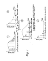
- the discrete Fourier transformation (DFT) of is for example, as shown an Fig. 1-1.
- a square wave having a basic angular frequency K ⁇ (0 ⁇ k ⁇ N-1) has a DFT as shown in Fig. 1-2.
- the waveform obtained from the result of the discrete convolution of these waveforms has a DFT as shown in Fig. 1-3.
- the DFT as shown in Fig. 1-4 is obtained.
- the basic frequency component of angular frequency ⁇ in Fig. 1- 4 is the DFT of the input signal, that is, the Kth DFT component X k in Fig. 1-1.
- the basic frequency component of angular frequency ⁇ in Fig. 1- 4 is the DFT of the input signal, that is, the Kth DFT component X k in Fig. 1-1.
- the odd order higher harmonic components 3 ⁇ , 5 ⁇ , Across appearing in Fig. 1-4 are removed by using a digital filter such as formed by several comb filters in cascade, and a sine wave having an angular frequency ⁇ is obtained.
- a digital filter such as formed by several comb filters in cascade
- the amplitude of the sine wave corresponds to
- the phase angle thereof corresponds to arg (X k ).
- the above-mentioned discrete convolution can be executed over one period of the sine wave, that is, the section (period) 2 ⁇ /k ⁇ . This can be carried out by multiplying with a matrix H k (representing a square wave) shown in equation (1).
- H k presents a square wave
- j ⁇ (k ⁇ j ⁇ (N-l)k) is obtained by successively shifting the elements in H
- the waveform formed by the sampled values at point N, obtained from the results of the discrete convolution is expressed as [W k (0), W k (1), whereas W k (N-1)].
- Equation (2) This is vectorized and expressed as W
- equation (2) can be executed by N 2 /2 additions. This number of additions can be decreased by the following method.
- Equation (3) it is assumed that the suffixes i, j, which denote the matrix, start from 0 and end at N-1.
- the signal shown by equation (4) is obtained by multiplying the matrix ⁇ H k and;. This signal is expressed as [ ⁇ W k (0), ⁇ W k (1), ... ⁇ W k (n-1)] as shown at the right side of equation (4).
- W k (N-1) when W k (N-1) is known, W k (0) is obtained from the following equation. Further, when Wk(0) is known, W k (1) is obtained from the following equation. That is, when ⁇ W k (n) (0 ⁇ n ⁇ N-1) is added to W k (N-1) successively, W k (0), W k (1), Vietnamese are obtained successively.
- W k (N-1) which is known at the beginning, can be obtained by calculating equation (2) with respect to only the (N-1)'th column of H k . This requires N/2 additions. Further, when ⁇ W k (n) is obtained from equation (4), 2N additions and subtractions are required.
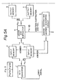
- FIG. 5 The construction of an embodiment of an apparatus according to the present invention is shown in Fig. 5.
- an input signal is converted by an analog-to-digital (A/D) converter 1 to a digital signal.
- This digital signal corresponds to Fig. 1-1, that is [x(0), x(l), Vietnamese, x(N-1)], and is written in one of two memories 2 and 3.
- the two memories are provided so that the input signal can be received smoothly when one memory is occupied by providing a signal for an adding and subtracting circuit 4.
- the two memories may each be alternately operated to read the input signal and to write a signal to the adding and subtracting circuit.
- An adding/subtracting address generation circuit 5 generates the matrix [H k ] shown in Fig. 1-2, that is, expressed by equation (1).
- the adding and subtracting circuit 4 calculates the product by the addition and subtraction process (as mentioned above).
- the ouput of the circuit 4 corresponds to Fig. 1-3.
- the adding and subtracting circuit 4 first executes equation (2) on the (N-1)'th column for in the input memory so as to calculate W k (N-1). Second, based on this W k (N-1) and using the above-mentioned difference conversion matrix, the circuit 4 calculates all the value [W k (0), W k (1), . ., W k (N-1)]. By this, the convolution waveform of the input signal and the square wave shown in equation (2) can be obtained. In the calculating process, addition or subtraction is selected by an address generation circuit 5 shown in Fig. 5. The obtained waveform is successively transferred to an output memory 6 or 7.
- Two output memories are provided for a similar reason as with the two input memories, that is, to allow input (writing) of the content of one memory to a digital filter 8, while the other output memory may be occupied by (reading from) the adding and sutracting circuit.
- Each output memory may alternate between these two types of operation.
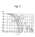
- a filter formed by a cascading comb filter 8a shown in Fig. 6A is used.
- the characteristic of the comb filter is shown in Fig. 6B.
- N/2n delayed samplings in the comb filter for removing n'th harmonics (n is 3.or higher odd number).
- N/2 is not always an integer.
- N/2n is rounded off.
- the cascaded comb filter is limited to a finite number (of comb filters).
- the rounding off of N/2n and the finite number of comb filters results in some error in the DFT obtained by the present invention.
- the error with comb filters for removing an m'th higher harmonic (m is 3 or a higher odd number) is as shown in Fig. 6C when (m-l)/2 comb filters are used. As shown in Fig. 6C, when seven cascaded comb filters are used for removing the 3rd to the 15th higher harmonic, the error becomes lower than 1%.
- the sine wave output from the comb filter 8 is, over the range of one period, input to a peak value detecting circuit 9 and a zero cross point detecting circuit 10 to obtain the amplitude and phase angle thereof.
- a moving average filter can also be used as the digital filter besides (instead of) a comb filter.
- the process can be carried out, using only adding and subtracting operations, by the operation of successively shifting a series of sampled values and averaging each determined number.
- the DFT of the input signal can be obtained by only a few addition and subtraction operations.
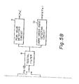
- Figure 8 shows another embodiment of the present invention.
- the embodiment is different from Fig. 5 in that a plurality of portions corresponding to Fig. 5 with the exception of the A/D converter 1, are arranged in parallel.
- the same portions as Fig. 5 are given the same reference numerals with suffixes a, b, and c.
- k' is set in the adding and subtracting address generator circuit 5 so as to carry out another operation.
- the values DFT component with respect to a plurality of k / can be calculated in parallel as shown in Fig. 8.
- sequential processing similar to Fig. 5 is possible and, usually, combined parallel and sequential processing is possible.
- theprocessing time can be decreased by 1/P, compared with when the same number values of k value are processed by the embodiment shown in Fig. 5.
- k'th components DFT (0 ⁇ k ⁇ N-l) can be obtained for an input signal [x(0), x(1), . ., x(N-1)] formed by N sample values with only 5215 N adding and subtracting processes and a digital filter. Therefore, DFT can be carried out in real time by a very simple apparatus which uses no multiplier.
Landscapes
- Physics & Mathematics (AREA)
- Engineering & Computer Science (AREA)
- General Physics & Mathematics (AREA)
- Mathematical Physics (AREA)
- Computational Mathematics (AREA)
- Mathematical Analysis (AREA)
- Mathematical Optimization (AREA)
- Pure & Applied Mathematics (AREA)
- Data Mining & Analysis (AREA)
- Theoretical Computer Science (AREA)
- Discrete Mathematics (AREA)
- Algebra (AREA)
- Databases & Information Systems (AREA)
- Software Systems (AREA)
- General Engineering & Computer Science (AREA)
- Complex Calculations (AREA)
Applications Claiming Priority (2)
| Application Number | Priority Date | Filing Date | Title |
|---|---|---|---|
| JP166861/83 | 1983-09-10 | ||
| JP58166861A JPH0230539B2 (ja) | 1983-09-10 | 1983-09-10 | Risanfuuriehenkansochi |
Publications (1)
| Publication Number | Publication Date |
|---|---|
| EP0137730A2 true EP0137730A2 (fr) | 1985-04-17 |
Family
ID=15838998
Family Applications (1)
| Application Number | Title | Priority Date | Filing Date |
|---|---|---|---|
| EP19840306158 Withdrawn EP0137730A2 (fr) | 1983-09-10 | 1984-09-10 | Méthode pour transformation discrète de Fourier et appareil pour l'effectuer |
Country Status (2)
| Country | Link |
|---|---|
| EP (1) | EP0137730A2 (fr) |
| JP (1) | JPH0230539B2 (fr) |
Cited By (2)
| Publication number | Priority date | Publication date | Assignee | Title |
|---|---|---|---|---|
| EP0458148A3 (en) * | 1990-05-09 | 1991-12-11 | Omron Corporation | Angle of rotation detector |
| EP1526414A4 (fr) * | 2002-08-01 | 2008-04-23 | Pioneer Corp | Systeme d'enregistrement et de lecture d'un hologramme |
-
1983
- 1983-09-10 JP JP58166861A patent/JPH0230539B2/ja not_active Expired - Lifetime
-
1984
- 1984-09-10 EP EP19840306158 patent/EP0137730A2/fr not_active Withdrawn
Cited By (3)
| Publication number | Priority date | Publication date | Assignee | Title |
|---|---|---|---|---|
| EP0458148A3 (en) * | 1990-05-09 | 1991-12-11 | Omron Corporation | Angle of rotation detector |
| US5455498A (en) * | 1990-05-09 | 1995-10-03 | Omron Corporation | Angle of rotation detector |
| EP1526414A4 (fr) * | 2002-08-01 | 2008-04-23 | Pioneer Corp | Systeme d'enregistrement et de lecture d'un hologramme |
Also Published As
| Publication number | Publication date |
|---|---|
| JPS6063676A (ja) | 1985-04-12 |
| JPH0230539B2 (ja) | 1990-07-06 |
Similar Documents
| Publication | Publication Date | Title |
|---|---|---|
| US3980873A (en) | Digital convolutional filter | |
| US4866647A (en) | Continuously variable digital delay circuit | |
| US3789199A (en) | Signal mode converter and processor | |
| US4843581A (en) | Digital signal processor architecture | |
| EP0373468B1 (fr) | Processeur pipeline pour mettre en oeuvre l'algorithme de LMS | |
| US4563750A (en) | Fast Fourier transform apparatus with data timing schedule decoupling | |
| US3925646A (en) | Information and process control enhancement system employing series of square wave components | |
| EP0137730A2 (fr) | Méthode pour transformation discrète de Fourier et appareil pour l'effectuer | |
| JP3522492B2 (ja) | 複素係数乗算器および複素係数フィルタ | |
| US4020333A (en) | Digital filter for filtering complex signals | |
| JPH0831776B2 (ja) | デジタルフイルタ | |
| US4118784A (en) | Differential DFT digital filtering device | |
| US5233549A (en) | Reduced quantization error FIR filter | |
| KR960018874A (ko) | 승산기 및 디지탈필터 | |
| JP2732673B2 (ja) | 離散的コサイン変換装置 | |
| US5309385A (en) | Vector division processing method and system | |
| JP2526990B2 (ja) | 非巡回形ダウンサンプリングフィルタ | |
| JP2622962B2 (ja) | Fftアナライザのズーミング装置 | |
| RU2119242C1 (ru) | Цифровой трансверсальный фильтр | |
| US4706188A (en) | Method and apparatus for reading samples of a time-dependent signal in a data processing system | |
| SU1488837A1 (ru) | Устройство скользящего спектрально-корреляционного анализа | |
| JPH10135742A (ja) | 信号波形発生装置 | |
| JPH0710411Y2 (ja) | 信号発生器 | |
| JPH06216715A (ja) | ディジタルフィルタ | |
| JPH0690137A (ja) | Firディジタルフィルタ |
Legal Events
| Date | Code | Title | Description |
|---|---|---|---|
| PUAI | Public reference made under article 153(3) epc to a published international application that has entered the european phase |
Free format text: ORIGINAL CODE: 0009012 |
|
| AK | Designated contracting states |
Designated state(s): DE FR GB |
|
| STAA | Information on the status of an ep patent application or granted ep patent |
Free format text: STATUS: THE APPLICATION HAS BEEN WITHDRAWN |
|
| 18W | Application withdrawn |
Withdrawal date: 19870806 |
|
| RIN1 | Information on inventor provided before grant (corrected) |
Inventor name: TAKAGI, TASUKU Inventor name: HARA, TOSHITO Inventor name: HAMADA, TAKASHI Inventor name: WAKATSUKI, NOBORU Inventor name: KOHATA, MINORU Inventor name: SONE, HIDEAKI |