EP0138026A2 - Elément pour retard de phase et prisme pour un système de mémorisation des données - Google Patents
Elément pour retard de phase et prisme pour un système de mémorisation des données Download PDFInfo
- Publication number
- EP0138026A2 EP0138026A2 EP84110537A EP84110537A EP0138026A2 EP 0138026 A2 EP0138026 A2 EP 0138026A2 EP 84110537 A EP84110537 A EP 84110537A EP 84110537 A EP84110537 A EP 84110537A EP 0138026 A2 EP0138026 A2 EP 0138026A2
- Authority
- EP
- European Patent Office
- Prior art keywords
- prism
- radiation
- thin film
- data storage
- optical data
- Prior art date
- Legal status (The legal status is an assumption and is not a legal conclusion. Google has not performed a legal analysis and makes no representation as to the accuracy of the status listed.)
- Ceased
Links
Images


Classifications
-
- G—PHYSICS
- G11—INFORMATION STORAGE
- G11B—INFORMATION STORAGE BASED ON RELATIVE MOVEMENT BETWEEN RECORD CARRIER AND TRANSDUCER
- G11B7/00—Recording or reproducing by optical means, e.g. recording using a thermal beam of optical radiation by modifying optical properties or the physical structure, reproducing using an optical beam at lower power by sensing optical properties; Record carriers therefor
- G11B7/12—Heads, e.g. forming of the optical beam spot or modulation of the optical beam
- G11B7/135—Means for guiding the beam from the source to the record carrier or from the record carrier to the detector
- G11B7/1365—Separate or integrated refractive elements, e.g. wave plates
-
- G—PHYSICS
- G02—OPTICS
- G02B—OPTICAL ELEMENTS, SYSTEMS OR APPARATUS
- G02B5/00—Optical elements other than lenses
- G02B5/30—Polarising elements
- G02B5/3083—Birefringent or phase retarding elements
Definitions
- This invention relates to optical components and more particularly to a phase retardation element for use in an optical data storage system.
- Phase retardation plates are widely used in optics to modify the polarization of a beam of light.
- optical data storage systems use a laser to generate a polarized beam of radiation. The beam is directed onto a rotating disk. The intensity of the reflected or transmitted beam varies according to the data recorded on the disk.
- a phase retardation plate is placed in the optical path to allow the use of a polarized beam splitter to deflect the reflected beam to a detector. Since the data tracks may be one micron in width, it is critical that the optical elements be precisely aligned. To this end, the incident and reflected beams share as much as possible of the optical system. The fewer components in the system, the better, since cost and reliability are improved.
- phase retardation element is the birefringent quarter wave plate which produces a phase difference of 90° between two perpendicular polarizations. It is used to transform linear polarized light into circular polarized and vice versa.
- a single order quarter wave plate is necessary for optical data storage system using a GaAs laser because of the center wavelength variation between lasers.
- phase shift was produced by reflection from a thin film structure. While the cost of such structures is less than a quarter wave plate, use of thin films in optical data storage systems introduced other complications. As the maximum phase shift obtained by external reflection from a periodic multilayer was less than 30°, at least four such reflections were required to obtain the desired phase shift of 90°. Alternatively, if an internal glass-air surface is used at least two internal reflections are necessary as has been realized in the Fresnel Rhomb. This adds to the cost and complicates the mounting and alignment to the point where any advantage over the quarter wave plate is lost. Moreover, the requirement that the reflectivity should be close to 100% for both polarizations limits the design freedom drastically.
- the principle object of the invention is to provide a thin film structure producing phase shift of 90° between two polarizations with a single internal reflection.
- Another object of the invention is to provide an optical data storage system which has an optical path incorporating a thin film on the surface of one of the elements to provide a phase shift of 90°.
- a further object of the invention is to reduce the number of optical elements in an optical data storage system by combining the thin film phase shift surface element with another element.
- FIG. 1 shows the optical path in a typical optical data storage system.
- Semiconductor laser 1 and collimating lens 2 generate a light beam 3 which is p - polarized and collimated but of elliptical cross-section. Projecting said light beam at an appropriate 0 onto prism 4 produces a light beam of circular cross-section propagating in the Y direction.
- Polarizing beam splitter 5 allows the p - polarized light beam to pass straight through toward quarter wave plate 6. Quarter wave plate 6 changes the polarization of the light beam onto circular.
- Lens 7 projects the light beam onto mirror-like surface of optical disk 8 where it is reflected back along the same path which it came.
- Quarter wave plate 6 now changes the circular polarization of the light beam to s - polarization.
- the s - polarized light beam is now reflected in the X direction at internal surface 9 of polarizing beam splitter 5.
- the surfaces of prism 4, polarizing beam splitter 5 and quarter wave plate 6 are coated with an anti-reflection film selected according to the angle of incidence and wavelength of the light beam.
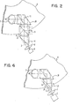
- FIG. 2 shows the optical system of FIG. 1 in which, according to the invention, quarter wave plate 6 has been replaced by a thin film retardation element 10 comprising a prism whose face 11 corresponding to the hypotenuse is coated by a conventional process with a thin film structure of a material of suitable index of refraction and thickness to effect the desired 90° phase retardation in the incident and return light beams.
- Prism 10 is rotated by 45° about the optical axis with respect to polarizing beam splitter 5 to resolve the light beam into two components.
- incident light beam 3 penetrates prism 10 it is totally reflected from the thin film structure at surface 11 of prism 10 and its polarization is changed to circular.
- Lens 7 projects the light beam ontio the surface of optical disk 8 where it is reflected back along the same path from which it came.
- the return light beam penetrates prism 10 it is totally reflected from the thin film structure at surface 11 of prism 10 and its polarization is changed (from circular) to s- polarized.
- Possible thin film structures are, for example, a single film of dielectric material, a multilayer film or a single metal film.
- FIG. 3 is a top view of polarizing beam splitter 5 and prism 10 from FIG. 2.
- a phase difference of 90° is obtainable for a film with a refractive index n F greater or equal to 2.05.
- n F refractive index
- the refractive index of the film one can select how fast the phase difference changes with a change of wavelengths.
- the retardation of the thin film quarter wave element can be much less dependent on wavelength.
- a specific performance can be designed.
- the solid curve in FIG. 5 also gives the performance for an optimized single layer film.
- Phase retardation can also be obtained from a prism coated with a single metal film.
- the advantage of the metal film is its uncritical thickness.
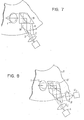
- the function of prism 4 can be combined with that of polarizing beam splitter 5 by simply cutting the entrance face 12 of polarizing beam splitter 5 at the same angle as used in prism 4 to obtain prism 13, shown in FIG. 6, and bonding phase retardation element 10 to prism 13 with an appropriate index matching adhesive. This eliminates four glass-t-air interfaces, thereby improving optical efficiency.
- prism 16 represents a further improvement obtained by combining the anti-reflection coating of surface 14 and the polarizing beam splitter coating of interface 15 of polarizing beam splitter 13 shown in FIG. 6.
- This combined coating 20 can be, for example, a multiplayer stack of material having alternatingly higher and lower indices of refraction.
- FIG. 8 shows an overall view of an optical data storage system incorporating a prism formed by combining prism 10 and prism 16 in a unitary structure 17, thereby eliminating another bonded interface.
- Laser 1 and collimating lens 2 generate a collimated light beam of elliptical cross-section which is projected at an appropriate angle onto prism 17.
- Prism 17 combines the functions of prism 4, polarizing beam splitter 5 and thin film phase retardation element 10 shown in FIG. 2. After emerging from prism 17, the return light beam is relayed to detector 19 by, for example, lens 18.
- Detector 19 may be composed of four or more sectors to extract data, tracking and focus information from the light beam.
Landscapes
- Physics & Mathematics (AREA)
- Optics & Photonics (AREA)
- General Physics & Mathematics (AREA)
- Polarising Elements (AREA)
- Optical Head (AREA)
Applications Claiming Priority (2)
| Application Number | Priority Date | Filing Date | Title |
|---|---|---|---|
| US06/541,604 US4595261A (en) | 1983-10-13 | 1983-10-13 | Phase retardation element and prism for use in an optical data storage system |
| US541604 | 1983-10-13 |
Publications (2)
| Publication Number | Publication Date |
|---|---|
| EP0138026A2 true EP0138026A2 (fr) | 1985-04-24 |
| EP0138026A3 EP0138026A3 (en) | 1987-08-19 |
Family
ID=24160281
Family Applications (1)
| Application Number | Title | Priority Date | Filing Date |
|---|---|---|---|
| EP84110537A Ceased EP0138026A3 (en) | 1983-10-13 | 1984-09-05 | Phase retardation element and prism for use in an optical data storage system |
Country Status (3)
| Country | Link |
|---|---|
| US (1) | US4595261A (fr) |
| EP (1) | EP0138026A3 (fr) |
| JP (1) | JPS6088903A (fr) |
Cited By (2)
| Publication number | Priority date | Publication date | Assignee | Title |
|---|---|---|---|---|
| EP0399650A3 (fr) * | 1989-05-22 | 1991-02-27 | Hewlett-Packard Company | Arrangement de prisme en forme de coin pour mémorisaton des informations |
| EP0579843A4 (en) * | 1992-02-07 | 1996-05-08 | Sony Corp | Phase varying device, and optical pickup apparatus using the same for magneto-optical storage |
Families Citing this family (5)
| Publication number | Priority date | Publication date | Assignee | Title |
|---|---|---|---|---|
| GB8720923D0 (en) * | 1987-09-05 | 1987-10-14 | Emi Plc Thorn | Optical image rotators |
| JPH04191703A (ja) * | 1990-11-27 | 1992-07-10 | Fujitsu Ltd | 偏光無依存性光学部品 |
| US5491580A (en) * | 1992-12-17 | 1996-02-13 | The United States Of America As Represented By The Secretary Of The Air Force | High power multilayer stack quarter wave plate |
| JPH06254110A (ja) * | 1993-03-01 | 1994-09-13 | Michihiro Tamura | 植毛用材料とその製造方法 |
| US6398364B1 (en) | 1999-10-06 | 2002-06-04 | Optical Coating Laboratory, Inc. | Off-axis image projection display system |
Family Cites Families (8)
| Publication number | Priority date | Publication date | Assignee | Title |
|---|---|---|---|---|
| US2409407A (en) * | 1943-02-22 | 1946-10-15 | Bausch & Lomb | Reflecting element for polarized light |
| US3703330A (en) * | 1971-06-15 | 1972-11-21 | Us Navy | Optical rotary joint |
| JPS526093B2 (fr) * | 1972-02-29 | 1977-02-18 | ||
| JPS5740481B2 (fr) * | 1972-10-04 | 1982-08-27 | ||
| US4084883A (en) * | 1977-02-28 | 1978-04-18 | The University Of Rochester | Reflective polarization retarder and laser apparatus utilizing same |
| JPS5546706A (en) * | 1978-09-29 | 1980-04-02 | Canon Inc | Phase difference reflecting mirror |
| US4312570A (en) * | 1979-09-14 | 1982-01-26 | Rockwell International Corporation | High reflectivity coated mirror producing 90 degree phase shift |
| US4406520A (en) * | 1980-08-14 | 1983-09-27 | Universal Pioneer Corporation | Beam splitter optical system of signal pickup device |
-
1983
- 1983-10-13 US US06/541,604 patent/US4595261A/en not_active Expired - Fee Related
-
1984
- 1984-09-05 EP EP84110537A patent/EP0138026A3/en not_active Ceased
- 1984-09-13 JP JP59190717A patent/JPS6088903A/ja active Granted
Cited By (2)
| Publication number | Priority date | Publication date | Assignee | Title |
|---|---|---|---|---|
| EP0399650A3 (fr) * | 1989-05-22 | 1991-02-27 | Hewlett-Packard Company | Arrangement de prisme en forme de coin pour mémorisaton des informations |
| EP0579843A4 (en) * | 1992-02-07 | 1996-05-08 | Sony Corp | Phase varying device, and optical pickup apparatus using the same for magneto-optical storage |
Also Published As
| Publication number | Publication date |
|---|---|
| US4595261A (en) | 1986-06-17 |
| JPH0139561B2 (fr) | 1989-08-22 |
| JPS6088903A (ja) | 1985-05-18 |
| EP0138026A3 (en) | 1987-08-19 |
Similar Documents
| Publication | Publication Date | Title |
|---|---|---|
| US4885734A (en) | Diffraction grating using birefringence and optical head in which a linearly polarized beam is directed to a diffraction grating | |
| US5659531A (en) | Optical head device and birefringent diffraction grating polarizer and polarizing hologram element used therein | |
| JP2644829B2 (ja) | 光情報記録再生装置 | |
| US5978346A (en) | Optical head | |
| US6005835A (en) | Composite prism and optical pickup using the same | |
| KR920010621B1 (ko) | 광학부품용기재와그의제조방법및그를사용한광학제품 | |
| JP3029541B2 (ja) | 光ピックアップ装置 | |
| EP0138026A2 (fr) | Elément pour retard de phase et prisme pour un système de mémorisation des données | |
| US5473594A (en) | Optical pickup device using optical lens coated with antireflection film whose spectral reflectance changes in accordance with wavelength | |
| US4553229A (en) | Apparatus for reading information | |
| JP3545008B2 (ja) | 光ピックアップ装置 | |
| JP2658818B2 (ja) | 複屈折回折格子型偏光子及び光ヘッド装置 | |
| JP3212105B2 (ja) | 光学ヘッド | |
| JPH09145924A (ja) | 光学素子と光ヘッド | |
| KR100219669B1 (ko) | 광픽업장치 | |
| US5168489A (en) | Recorded data reader employing a polarized beam splitter | |
| JPH09145922A (ja) | 回折用光学素子およびこれを用いた光ピックアップ装置 | |
| JP2996856B2 (ja) | 光学式ピックアップ装置 | |
| KR100188963B1 (ko) | 광픽업장치 | |
| JPH09167375A (ja) | ビーム整形プリズムおよびこれを有する光ヘッド装置 | |
| JP2725324B2 (ja) | 光記録媒体用光ヘッド | |
| JP2002287093A (ja) | 光アイソレータ | |
| KR0131372B1 (ko) | 광디스크용 광픽업의 위상보정 박막설계방법 | |
| JP3393680B2 (ja) | 光ピックアップ | |
| JPH069089B2 (ja) | 光ヘツド |
Legal Events
| Date | Code | Title | Description |
|---|---|---|---|
| PUAI | Public reference made under article 153(3) epc to a published international application that has entered the european phase |
Free format text: ORIGINAL CODE: 0009012 |
|
| 17P | Request for examination filed |
Effective date: 19841123 |
|
| AK | Designated contracting states |
Designated state(s): DE FR GB |
|
| PUAL | Search report despatched |
Free format text: ORIGINAL CODE: 0009013 |
|
| AK | Designated contracting states |
Kind code of ref document: A3 Designated state(s): DE FR GB |
|
| 17Q | First examination report despatched |
Effective date: 19890209 |
|
| STAA | Information on the status of an ep patent application or granted ep patent |
Free format text: STATUS: THE APPLICATION HAS BEEN REFUSED |
|
| 18R | Application refused |
Effective date: 19921207 |
|
| APAF | Appeal reference modified |
Free format text: ORIGINAL CODE: EPIDOSCREFNE |
|
| RIN1 | Information on inventor provided before grant (corrected) |
Inventor name: SPILLER, EBERHARD ADOLPH Inventor name: LUECKE, FRANCIS STEPHEN Inventor name: BAASCH, HOLGER JOHAN Inventor name: GOODMAN, DOUGLAS SEYMORE Inventor name: SODERSTROM, RONALD LEE |