EP0138276A2 - Gesteuerte Oszillatorschaltung - Google Patents
Gesteuerte Oszillatorschaltung Download PDFInfo
- Publication number
- EP0138276A2 EP0138276A2 EP84201456A EP84201456A EP0138276A2 EP 0138276 A2 EP0138276 A2 EP 0138276A2 EP 84201456 A EP84201456 A EP 84201456A EP 84201456 A EP84201456 A EP 84201456A EP 0138276 A2 EP0138276 A2 EP 0138276A2
- Authority
- EP
- European Patent Office
- Prior art keywords
- circuit
- signal
- output
- delay
- controlled oscillator
- Prior art date
- Legal status (The legal status is an assumption and is not a legal conclusion. Google has not performed a legal analysis and makes no representation as to the accuracy of the status listed.)
- Granted
Links
Images


Classifications
-
- H—ELECTRICITY
- H03—ELECTRONIC CIRCUITRY
- H03L—AUTOMATIC CONTROL, STARTING, SYNCHRONISATION OR STABILISATION OF GENERATORS OF ELECTRONIC OSCILLATIONS OR PULSES
- H03L5/00—Automatic control of voltage, current, or power
-
- H—ELECTRICITY
- H03—ELECTRONIC CIRCUITRY
- H03L—AUTOMATIC CONTROL, STARTING, SYNCHRONISATION OR STABILISATION OF GENERATORS OF ELECTRONIC OSCILLATIONS OR PULSES
- H03L7/00—Automatic control of frequency or phase; Synchronisation
- H03L7/06—Automatic control of frequency or phase; Synchronisation using a reference signal applied to a frequency- or phase-locked loop
- H03L7/08—Details of the phase-locked loop
- H03L7/081—Details of the phase-locked loop provided with an additional controlled phase shifter
- H03L7/0812—Details of the phase-locked loop provided with an additional controlled phase shifter and where no voltage or current controlled oscillator is used
- H03L7/0814—Details of the phase-locked loop provided with an additional controlled phase shifter and where no voltage or current controlled oscillator is used the phase shifting device being digitally controlled
-
- H—ELECTRICITY
- H03—ELECTRONIC CIRCUITRY
- H03L—AUTOMATIC CONTROL, STARTING, SYNCHRONISATION OR STABILISATION OF GENERATORS OF ELECTRONIC OSCILLATIONS OR PULSES
- H03L7/00—Automatic control of frequency or phase; Synchronisation
- H03L7/06—Automatic control of frequency or phase; Synchronisation using a reference signal applied to a frequency- or phase-locked loop
- H03L7/08—Details of the phase-locked loop
- H03L7/099—Details of the phase-locked loop concerning mainly the controlled oscillator of the loop
- H03L7/0991—Details of the phase-locked loop concerning mainly the controlled oscillator of the loop the oscillator being a digital oscillator, e.g. composed of a fixed oscillator followed by a variable frequency divider
- H03L7/0992—Details of the phase-locked loop concerning mainly the controlled oscillator of the loop the oscillator being a digital oscillator, e.g. composed of a fixed oscillator followed by a variable frequency divider comprising a counter or a frequency divider
- H03L7/0993—Details of the phase-locked loop concerning mainly the controlled oscillator of the loop the oscillator being a digital oscillator, e.g. composed of a fixed oscillator followed by a variable frequency divider comprising a counter or a frequency divider and a circuit for adding and deleting pulses
Definitions
- the invention relates to a controlled oscillator circuit having an input for receiving a control signal and an output for supplying a clock signal.
- Such an oscillator is employed in inter alia phase-locked loops.
- the oscillator For some uses, such as the reproduction of digital information from a record carrier, in particular an optically readable record carrier for "compact-disc digital audio" the oscillator must be locked to the channel- bit frequency of the reproduced signal and must be capable of following variations of said channel bit frequency in a sufficiently rapid and accurate manner. For the large-scale integration of components it may then be advantageous if this controlled oscillator circuit can be constructed largely in digital technology.
- the oscillator circuit in accordance with the invention may be further characterized in that the tuning-control circuit is a divider with a variable divisor which is adjusted in conformity with the output signal of the rounding circuit.
- tuning-control circuit comprises a variable delay network, which alternative has the advantage that lower frequencies and consequently a slower logic may be employed.
- variable delay network comprises a plurality of n delay networks with a delay time which are arranged in series in the output circuit of an oscillator operating with a fixed frequency fo, (n+1) ⁇ being equal to one period of the frequency fo, and the output is connectable to outputs of the delay networks as a function of the output signal of the rounding circuit in such a manner that switching is possible from the output of the last delay network to the input of the first delay network.
- this embodiment may be further characterized in that there is provided a phase-comparator circuit for comparing the phase of the signals on two points in the chain of delay networks and the delay networks are adjustable by said phase-comparator circuit in such a manner that the phase shift corresponding to a time delay ⁇ at the frequency fo is 360/(n+1) 0 .
- an additional delay network with a time delay ⁇ is arranged in the chain of delay networks in series with the chain of n delay networks and the phase-comparison circuit controls the overall phase variation of all n+1 networks in such a manner that it is equal to 360°.
- this embodiment may be characterized in that the circuit comprises a (n+1)-position switch whose (n+1) inputs are connected to (n+1) terminals of the delay networks in a cyclic sequence, which terminals are connected to the input of the first of the n networks and the outputs of all n networks in a cyclic sequence and the output is connected to the output of the controlled oscillator circuit, and the output signal of the rounding circuit controls the switch via a counter with n+1 positions, which counter is operated cyclically, the count of said counter determining which of the n+1 terminals is connected to the output of the controlled oscillator circuit by said switch.
- a disc-shaped record carrier 1 is shown in a schematic cross-sectional view.
- This record carrier comprises a substrate 2 in which a track structure is formed, which structure comprises pits 3 and intermediate areas 4.
- This relief type track structure is coated with a reflecting layer 5 and a transparent protective layer 6.
- the information contained in the relief-type track structure is read in that a laser beam generated by a laser 7 is projected and focused on the tracks via a lens system 8, the reflected beam being projected on an in-line array of four optical detectors 11a, 11b, 11c and 11d via a semi-transparent mirror 9 and a beam splitter 10.
- the currents supplied by these photodetectors are converted into the signal voltages V 1 , V 2 , V 3 and V 4 by means of a current-voltage converter 12.
- the focusing of the lens system 8 is controlled in a manner, not shown, by means of a focusing control signal FE'.
- a radial control signal RE' For radial tracking the radial location of the spot produced by the laser beam is controlled by means of a radial control signal RE'. This is a fine-control system. Coarse control is obtained (in a manner not shown) by moving the entire optical system 7, 8, 9, 10, 11 in a radial direction under command of a control signal CE'.
- the control signals CE', RE' and FE' are derived from the signal voltages V 1 , V 29 V 3 and V 4 .
- the signal (V 1 + V 4 ) - (V 2 + V 3 ) is required for the signal FE' and the signal (V + V 2 ) - (V 3 + V 4 ) is required for the signal CE' and the signal RE'.
- All these control signals can be derived from three signals A', B' and C' which are obtained by combining the signals V 1 , V 2 , V 3 and V 4 . In the present embodiment these signals are related as follows:
- the combination of the signals V1, V 2 , V 3 and V 4 described in the foregoing is obtained by means of a matrix 13.
- This combination has the advantage that only three instead of four signals must be digitized, so that a lower local clock frequency can be used than would be the case if these signals are digitized serially.
- the signals A', B' and C' are converted into serial form by means of a multiplexer 14, they are digitized in an analog-to-digital converter 15 and they are reconverted into parallel form to obtain the corresponding digital samples A, B and C by means of a demultiplexer 16.
- the multiplexer 14, the analog-to-digital converter 15 and the demultiplexer 16 receive clock signals from a clock-signal generating circuit 17, which supplies the required clock signals in the correct phase relationship under control of an oscillator 18, in such a manner that the samples A, B and C are supplied in synchronism with the bit frequency of the data signal.
- the various control signals it is important to suppress the data-signal spectrum as far as possible. This is achieved by selecting samples in synchronism with the data pattern (pits and intermediate areas), so that the instantaneous sampling frequency becomes equal to the instantaneous frequency of the data signal. For this purpose one sample for each pit (3) and for each intermediate area (4) is selected from each of the samples A, B and C and, in order to minimize the effect of the optical transfer function of the read-out (the signal amplitude is a function of the location of the projected laser beam relative to the pits and decreases towards the edges of the pits), the samples are taken only for pits and intermediate areas which are longer than a specific number of clock periods, in the present example longer than 5 clock periods.
- a detector 19 (which will be described in more detail with reference to Fig. 2) generates a pulse on an output 20 when the sixth sample in one pit is detected and a pulse on output 21 when the sixth sample in one intermediate area is detected.
- the detector 19 receives the clock signals from the oscillator 18 on an input 22 and the digital sum of the signals A and B, obtained by means of the adder 25 and equalized by means of the circuit 24, on an input 23.
- the samples A, B and C are each delayed by three clock periods ( T ) of the oscillator 18 by means of delay networks 26, 27 and 28 respectively, are equalized by means of the equalizers 29, 30 and 31 respectively, and are applied to the hold circuits 32 and 33, 34 and 35, and 36 respectively.
- the hold circuits 32, 34 and 36 are clocked by the signal on output 21 of the detector 19 and the hold circuits 33 and 35 by the signal on output 20.
- the signals a, a, b, b and c are applied to a processing circuit 37, which supplies the signals RE, CE and FE on outputs 43, 44 and 45 respectively, and a signal TL representing a loss of track, a signal DO indicating a signal drop-out, a signal HFL indicating that the level of the high-frequency data signal is too low, and a signal SL which is a decision level for the data-signal processing, on outputs 46, 47, 48 and 49, respectively.
- the signals RE, CE and FE are converted into analog signals by means of digital-to-analog converters 50, 51 and 52 and subsequently they are amplified by the amplifier 53, 54 and 55 to form the analog control signals RE', CE' and FE' for focusing and tracking control.
- the sum of the signals A + B formed by means of the adder 25 and the equalizer 24 is not only applied to a detector 19 but also to a comparator 56 which also receives the decision level SL for restoring the digital data signal and applying it to an output 57 and to a phase comparator circuit 58, which compares the phase of the samples A + B with the phase of the data signal on the record carrier 1 and which supplies a signal which is a measure of this phase to an output 59 and a signal which is a measure of the assymetry of the signal A + B to an output 60, which last-mentioned signal is applied to a circuit 37.
- the phase-error signal on output 59 controls the oscillator 18 via a low-pass filter 61.
- Fig. 2 shows an example of the detector 19 in the apparatus shown in Fig. 1, and Fig. 3 shows some diagrams to explain the operation of the circuit shown in Fig. 2.
- the signal A + B from the equalizer 24 is applied to a high-pass filter 62 via an input 23 in order to remove the low-frequency components, thereby enabling the digital data signal to be restored by means of a simple comparator 63.
- the edges of the rectangular data signal are detected by means of a circuit 64, for example a differentiator.
- This edge detector starts a counter 65 which counts the clock pulses (from the oscillator 18) on its input 22 from the instant defined by the pulses from the edge detector 64.
- a decoder circuit 66 decodes a specific count, in the present example six, When the count "six" is reached, the pulses are applied to AND-gates 67 and 68. The gate 67 also receives the restored data signal on an inverting input and the gate 68 receives this signal on a non-inverting input. As a result of this, a pulse will appear on output 21 when the count "six" is reached during a positive data signal (3c) and on output 20 when the count "six" is reached during a negative data signal.
- Fig. 3a shows a part of a data track on the record carrier, which track comprises pits 3 and intermediate areas 4 between these pits.
- Fig. 3b shows the samples A + B originating from the track shown in Fig. 3a.
- Fig. 3c shows the restored data signal after the comparator 63, which is a substantially rectangular signal with a period corresponding to the length of the pits and intermediate areas.
- Fig. 3d shows the starting pulses for the counter 65 formed on the edges of the data signal, which counter counts the pulses of the clock signal shown in Fig. 3e.
- the counter 65 supplies a pulse each time that the count "six" is reached and for a positive data signal (Fig. 3c), i.e.
- a pulse will appear on output 21 (Fig. 3f), whilst for a negative data signal, i.e.during a pit, the pulse will appear on output 20 (Fig. 3g).
- the signals A, B and C which have been delayed by three clock periods, are thus sampled.
- Fig. 3h shows the signal A which has been delayed by three clock periods and for which the hold circuit 32 (Fig. 1) holds the third sample from each intermediate area longer than five clock periods (signal shown in Fig. 3i) the sample and hold circuit 33 holds the third sample from each pit longer than five clock periods (signal shown in Fig. 3j).
- the clock frequency which is locked to the edges of the data signal on the disc is not very stable, but exhibits a variation (jitter) of approximately 50 nsecs.
- the clock oscillator 18 (Fig. 1) must be capable of accuratdy keeping in track with this jitter; in practice a tracking accuracy of 10 to 15 nsecs. (for a period of + 200 nsecs.) is found to be adequate.
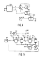
- Fig. 4 shows an example of an oscillator circuit 18 having this tracking accuracy.
- the phase-error signal from the lo % -pass filter 61 is divided into m steps by means of the rounding circuit 100, which steps correspond to the tracking accuracy of 10 to 15 nsecs. (one step of 10 nsecs for a clock signal with a period of 200 nsecs. corresponds to a phase difference of 18 0 ).
- the adder 103 adds this step to the output signal m of the rounding circuit 100.
- the output signal of this adder 103 i.e.the rounded phase error, controls the divisor of a variable divider 105, which divides the output signal of a fixed oscillator 104.
- a step of 10 nsecs for a desired clock signal with a period of approximately 200 nsecs. corresponds to 1/20 of the period of this clock signal, a signal may be used with a frequency of approximately 100 MHz and a divisor which can be varied around the value 20.
- On the output 99 of the divider a clock signal is obtained with a period of the order of 200 nsecs. (+ 5 MHz), which is variable in steps of approximately 10 nsecs.
- the circuit comprises a fixed oscillator 107 which is tuned to approximately the desired frequency (nominal 4.31 MHz).
- the output signal of this oscillator is passed through n delay networks 108 . to 108 , which each have a delay equal to the desired step size, i.e. 10 to 15 nsecs.
- the overall delay of the n networks must correspond to one period of the clock signal, for which purpose the output signal of the last network 108 n is compared with the output signal of the oscillator 107 by means of a phase comparator 109.
- the output signal of the phase comparator 109 controls the delay time of the networks 108 via an integrator 110, so that together these networks provide a delay of exactly one period of the clock signal.
- tappings 111 1 to 111 n are provided.
- one of the tappings 111 is selected via the accumulator 112.
- output 99 will scan the tappings 111 via the multiplexer 113 depending on the phase error and consequently on the frequency difference and start again after every n steps, which will not give rise to a discontinuity because n steps exactly correspond to one period of the output signal.
- the phase and frequency of the signal on output 99 is consequently the result of phase cmodulation of the signal from oscillator 107, which phase modulation is effected in discrete steps of 360/n°.
Landscapes
- Stabilization Of Oscillater, Synchronisation, Frequency Synthesizers (AREA)
- Channel Selection Circuits, Automatic Tuning Circuits (AREA)
Applications Claiming Priority (2)
| Application Number | Priority Date | Filing Date | Title |
|---|---|---|---|
| NL8303561A NL8303561A (nl) | 1983-10-17 | 1983-10-17 | Geregelde oscillatorschakeling. |
| NL8303561 | 1983-10-17 |
Publications (3)
| Publication Number | Publication Date |
|---|---|
| EP0138276A2 true EP0138276A2 (de) | 1985-04-24 |
| EP0138276A3 EP0138276A3 (en) | 1985-06-19 |
| EP0138276B1 EP0138276B1 (de) | 1988-02-10 |
Family
ID=19842568
Family Applications (1)
| Application Number | Title | Priority Date | Filing Date |
|---|---|---|---|
| EP84201456A Expired EP0138276B1 (de) | 1983-10-17 | 1984-10-10 | Gesteuerte Oszillatorschaltung |
Country Status (9)
| Country | Link |
|---|---|
| US (1) | US4568887A (de) |
| EP (1) | EP0138276B1 (de) |
| JP (1) | JPH0740667B2 (de) |
| KR (1) | KR920010214B1 (de) |
| DE (1) | DE3469331D1 (de) |
| ES (1) | ES536759A0 (de) |
| HK (1) | HK84591A (de) |
| NL (1) | NL8303561A (de) |
| SG (1) | SG49490G (de) |
Cited By (5)
| Publication number | Priority date | Publication date | Assignee | Title |
|---|---|---|---|---|
| GB2197553A (en) * | 1986-10-07 | 1988-05-18 | Western Digital Corp | Phase-locked loop delay line |
| GB2249230A (en) * | 1990-10-24 | 1992-04-29 | Burr Brown Corp | Synchronising circuit |
| EP0487902A3 (en) * | 1990-11-29 | 1993-06-30 | International Business Machines Corporation | Delay line calibration circuits |
| EP0803791A1 (de) * | 1989-07-07 | 1997-10-29 | STMicroelectronics Limited | Takterzeugungsschaltung |
| WO2002043246A1 (de) * | 2000-11-21 | 2002-05-30 | Micronas Gmbh | Phasenregelkreis mit verzögerungselement |
Families Citing this family (7)
| Publication number | Priority date | Publication date | Assignee | Title |
|---|---|---|---|---|
| EP0202773B1 (de) * | 1985-04-22 | 1991-01-16 | Csk Corporation | Binäres Kodierverfahren für Daten, welche von einer optischen Platte gelesen werden und Gerät dafür |
| NL8502802A (nl) * | 1985-10-14 | 1987-05-04 | Philips Nv | Inrichting voor het uitlezen en/of inschrijven van een optische spoorvormige informatiestruktuur. |
| JPH07118166B2 (ja) * | 1987-05-21 | 1995-12-18 | パイオニア株式会社 | トラッキング回路 |
| DE3810809A1 (de) * | 1988-03-30 | 1989-10-12 | Fev Motorentech Gmbh & Co Kg | Verfahren zur phasengekoppelten frequenzumsetzung |
| US6150855A (en) * | 1990-02-06 | 2000-11-21 | Bull, S.A. | Phase-locked loop and resulting frequency multiplier |
| DE69204144T2 (de) * | 1991-11-25 | 1996-03-21 | Philips Electronics Nv | Phasenregelschleife mit Frequenzabweichungsdetektor und Decodierschaltung mit einer solchen Phasenregelschleife. |
| US7430239B2 (en) * | 2001-11-30 | 2008-09-30 | Koninklijke Philips Electronics N.V. | Bit-detection arrangement and apparatus for reproducing information |
Family Cites Families (2)
| Publication number | Priority date | Publication date | Assignee | Title |
|---|---|---|---|---|
| FR1601909A (de) * | 1968-12-27 | 1970-09-21 | ||
| FR2448257A1 (fr) * | 1979-02-05 | 1980-08-29 | Trt Telecom Radio Electr | Dispositif de resynchronisation rapide d'une horloge |
-
1983
- 1983-10-17 NL NL8303561A patent/NL8303561A/nl not_active Application Discontinuation
-
1984
- 1984-02-09 US US06/578,461 patent/US4568887A/en not_active Expired - Fee Related
- 1984-10-10 DE DE8484201456T patent/DE3469331D1/de not_active Expired
- 1984-10-10 EP EP84201456A patent/EP0138276B1/de not_active Expired
- 1984-10-15 ES ES536759A patent/ES536759A0/es active Granted
- 1984-10-16 KR KR1019840006400A patent/KR920010214B1/ko not_active Expired
- 1984-10-17 JP JP59216457A patent/JPH0740667B2/ja not_active Expired - Lifetime
-
1990
- 1990-07-04 SG SG494/90A patent/SG49490G/en unknown
-
1991
- 1991-10-24 HK HK845/91A patent/HK84591A/xx unknown
Cited By (5)
| Publication number | Priority date | Publication date | Assignee | Title |
|---|---|---|---|---|
| GB2197553A (en) * | 1986-10-07 | 1988-05-18 | Western Digital Corp | Phase-locked loop delay line |
| EP0803791A1 (de) * | 1989-07-07 | 1997-10-29 | STMicroelectronics Limited | Takterzeugungsschaltung |
| GB2249230A (en) * | 1990-10-24 | 1992-04-29 | Burr Brown Corp | Synchronising circuit |
| EP0487902A3 (en) * | 1990-11-29 | 1993-06-30 | International Business Machines Corporation | Delay line calibration circuits |
| WO2002043246A1 (de) * | 2000-11-21 | 2002-05-30 | Micronas Gmbh | Phasenregelkreis mit verzögerungselement |
Also Published As
| Publication number | Publication date |
|---|---|
| ES8506952A1 (es) | 1985-08-01 |
| KR920010214B1 (ko) | 1992-11-21 |
| JPH0740667B2 (ja) | 1995-05-01 |
| EP0138276B1 (de) | 1988-02-10 |
| US4568887A (en) | 1986-02-04 |
| JPS60103731A (ja) | 1985-06-08 |
| HK84591A (en) | 1991-11-01 |
| NL8303561A (nl) | 1985-05-17 |
| EP0138276A3 (en) | 1985-06-19 |
| KR850003091A (ko) | 1985-05-28 |
| ES536759A0 (es) | 1985-08-01 |
| DE3469331D1 (en) | 1988-03-17 |
| SG49490G (en) | 1990-08-31 |
Similar Documents
| Publication | Publication Date | Title |
|---|---|---|
| US4813031A (en) | Apparatus for reproducing information from an optically readable record carrier | |
| KR870000280B1 (ko) | 펄스폭 변조회로 | |
| EP0096106B1 (de) | PLL-Steuerkreis | |
| EP0138276B1 (de) | Gesteuerte Oszillatorschaltung | |
| US4418406A (en) | Signal wave control circuit | |
| EP0098349B1 (de) | Frequenzdetektorschaltung für ein digitales Informationswiedergabesystem | |
| EP0138275B1 (de) | Gerät zur Wiedergabe von Informationen auf einem optisch lesbaren Informationsträger | |
| KR19980080386A (ko) | 디지털 신호 재생 회로 | |
| US6236628B1 (en) | Read channel circuit for optical disk reproducing apparatus | |
| EP0138274B1 (de) | Gerät zur Wiedergabe von digitalen Informationen via ein Übertragungsmedium | |
| US5786953A (en) | Arrangement for reproducing n digital signals having n phase-locked loops each including a phase shifter, controlled by an integrating element, arranged between a VCO output and a phase detector | |
| EP1005166B1 (de) | Verfahren zur Erfassung der Frequenz in einem digitalen Phasenregelkreis | |
| US6876707B2 (en) | Signal processing circuit and signal processing method | |
| KR100639403B1 (ko) | 기록매체 상의 트랙에/트랙으로부터 정보신호의 기록 및재생 | |
| US6879551B2 (en) | Apparatus and method for generating RF signal and control signals in optical disc system | |
| KR20010031917A (ko) | 클럭 리커버리 장치 | |
| KR100186394B1 (ko) | 광디스크 시스템의 비트클럭 회복장치 | |
| JPS59124013A (ja) | デ−タ再生装置 | |
| SU1663626A1 (ru) | Устройство дл многоканальной магнитной записи и воспроизведени сигналов | |
| JPH0294916A (ja) | データスライス回路 | |
| JPS59152513A (ja) | デジタルデ−タ生成装置 | |
| JPH0281324A (ja) | 再生信号補正方法 | |
| JPS59114614A (ja) | パルス幅変調回路 | |
| HK1013357B (en) | Arrangement for reproducing n digital signals from n adjacent tracks on a record carrier |
Legal Events
| Date | Code | Title | Description |
|---|---|---|---|
| PUAI | Public reference made under article 153(3) epc to a published international application that has entered the european phase |
Free format text: ORIGINAL CODE: 0009012 |
|
| PUAL | Search report despatched |
Free format text: ORIGINAL CODE: 0009013 |
|
| AK | Designated contracting states |
Designated state(s): BE DE FR GB |
|
| AK | Designated contracting states |
Designated state(s): BE DE FR GB |
|
| 17P | Request for examination filed |
Effective date: 19851218 |
|
| 17Q | First examination report despatched |
Effective date: 19861223 |
|
| GRAA | (expected) grant |
Free format text: ORIGINAL CODE: 0009210 |
|
| AK | Designated contracting states |
Kind code of ref document: B1 Designated state(s): BE DE FR GB |
|
| REF | Corresponds to: |
Ref document number: 3469331 Country of ref document: DE Date of ref document: 19880317 |
|
| ET | Fr: translation filed | ||
| PLBE | No opposition filed within time limit |
Free format text: ORIGINAL CODE: 0009261 |
|
| STAA | Information on the status of an ep patent application or granted ep patent |
Free format text: STATUS: NO OPPOSITION FILED WITHIN TIME LIMIT |
|
| 26N | No opposition filed | ||
| PGFP | Annual fee paid to national office [announced via postgrant information from national office to epo] |
Ref country code: GB Payment date: 19940930 Year of fee payment: 11 Ref country code: BE Payment date: 19940930 Year of fee payment: 11 |
|
| PGFP | Annual fee paid to national office [announced via postgrant information from national office to epo] |
Ref country code: FR Payment date: 19941026 Year of fee payment: 11 |
|
| PGFP | Annual fee paid to national office [announced via postgrant information from national office to epo] |
Ref country code: DE Payment date: 19941223 Year of fee payment: 11 |
|
| PG25 | Lapsed in a contracting state [announced via postgrant information from national office to epo] |
Ref country code: GB Effective date: 19951010 |
|
| PG25 | Lapsed in a contracting state [announced via postgrant information from national office to epo] |
Ref country code: BE Effective date: 19951031 |
|
| BERE | Be: lapsed |
Owner name: PHILIPS ELECTRONICS N.V. Effective date: 19951031 |
|
| GBPC | Gb: european patent ceased through non-payment of renewal fee |
Effective date: 19951010 |
|
| PG25 | Lapsed in a contracting state [announced via postgrant information from national office to epo] |
Ref country code: FR Effective date: 19960628 |
|
| PG25 | Lapsed in a contracting state [announced via postgrant information from national office to epo] |
Ref country code: DE Effective date: 19960702 |
|
| REG | Reference to a national code |
Ref country code: FR Ref legal event code: ST |